國 立 交 通 大 學
電信工程學系
碩 士 論 文
1.5 伏寬頻低失真通道選擇濾波器
1.5-V Wide-Band Low Distortion Channel
Selection Filter
研究生:楊峻岳
指導教授:洪崇智
1.5V 寬頻低失真通道選擇濾波器
1.5V Wide-Band Low distortion Channel
selection filter
研 究 生:楊 峻 岳
Student: Chun-Yueh Yang
指導教授:洪 崇 智 教授
Advisor: Prof. Chung-Chih Hung
國立交通大學
電信工程學系 電信研究所碩士班
碩 士 論 文
A Thesis
Submitted to Department of Communication Engineering
College of Electrical Engineering and Computer Science
National Chiao-Tung University
In Partial Fulfillment of the Requirements
For the Degree of
Master of Science
In
Communication Engineering
January 2006
Hsinchu, Taiwan, Republic of China
中華民國九十五年一月
1.5V 寬頻低失真通道選擇濾波器
學生:楊峻岳 指導教授:洪崇智
交通大學電信工程學系 (研究所) 碩士班
摘要
切換式電容濾波器的研究已經行之有年,在這方面的研究也相當的豐富。 自從切換式電容濾波器首次被應用在脈衝編碼調變的系統上,許多相關於切換式 電容濾波技術被快速的發展出來被應用到各種領域。隨著製程演進,切換式電容 濾波器也逐漸被應用到高速的通信電路。對於SC 的電路而言,動態範圍是評估 電路效能的一個重要指標。較大的動態範圍可以使得SC 電路有較高的位元數。 而SC 電路的動態範圍主要受到噪音和失真有兩個因素影響。許多關於噪音消除 技術如chopper stabilized 和三角積分架構已經都被證實能有效地降低噪音功 率。但是對於電路諧波失真的消除,依舊有著很大的改善空間。 此次研究主要在於使用TSMC 0.18µm 的製程來設計一個高速低電壓低失 真切換式電容濾波器。而設計低電壓的類比電路的主要目的是為了將類比電路和 數位電路整合一起以減少面積成本。在低電壓的狀況下,以往傳統的類比電路架 構都會遇到許多設計上的挑戰。信號的擺幅下降便是低電壓設計上的一大考驗, 同時也會降低整個電路的效能。另外對於濾波器本身我們也希望能夠提升其線性 度。因此經由許多架構上的考量以及關鍵元件的設計,可以有效的維持信號擺幅 以及大幅的降低信號失真。同時我們也提出了一個低失真的取樣開關,將此應用 在此次電路上藉以降低整個電路總諧波失真。1.5v Wide-Band Low Distortion Channel Selection filter
Student: Chun-Yueh Yang Advisor: Prof. Chung-Chih Hung
Abstract
The research for switched capacitor filter has been developed for many years and plentiful. Since the first time the switched capacitor was applied on PCM system, many switched capacitor filtering technique were proposed and applied on various fields. With the process improvement, the switched capacitor filter is used in high speed communication circuit increasingly. The dynamic range is a key performance for the switched capacitor circuit. The switched capacitor circuit with the larger dynamic range has more bits. The dynamic range is mainly affected by the noise and the distortion in the switched capacitor circuit. A lot of solutions, like chopper stabilized and delta sigma architecture, for reducing the noise power were proved their effectiveness. But there is few for declining the distortion.
We used the process, TSMC 0.18um, to design a high speed low voltage low distortion switched capacitor filter. The objective of low voltage analog circuit is for highly monolithic integration. But it makes the analog circuit more difficult. The signal swing would be reduced linearly by power supply. It would be affect the performance whole circuit. In addition, it is desired to raise the linearity of the filter. Through many design considerations and key component design, we can contribute the much less distortion. In the meanwhile, we proposed a novel low distortion MOS sampling switch applied on this filter for reducing THD.
誌謝
隨著碩士論文的完成,這十多年來求學生涯也即將接近尾聲。結束了漫長 的學生時代,我也將要向人生的下一個目標前進。首先感謝我的指導教授洪崇智 博士這兩年來的指導,給予首次嘗試類比電路設計的我許多指導與幫助。這兩年 來習得許多類比電路設計技巧以及實作上的考量,同時開始學習獨立思考和解決 問題的能力,這些都是有別於以往求學階段難以學習到的部份,這部份確實使我 獲益匪淺。同時也感謝國家晶片中心所提供的先進的半導體製程,能使我將所設 計的電路加以實現,也完成人生中第一篇的國際會議論文,和老師一同參加國際 會議是我畢生難忘的經驗。 另外要感謝邱俊宏、莊誌倫、張家瑋、李三益諸位同窗以及博士班學長羅 天佑,一起在實驗室奮鬥的時光令人難忘。特別對於一個剛起步的實驗室,許許 多多的辛苦和努力以及同甘共苦的革命情感,都是這兩年多來的點點滴滴。這些 日子來的互相砥礪和教學相長,都令我們成長不少。也感謝蔡宗諺、楊家泰、黃 琳家、林政翰、黃柏勳、何俊達等學弟許許多多生活上和課業上的幫助。 我也要特別感謝我的父母親,含辛茹苦將我們家中的三個孩子養育長大, 提供我們穩定而健全的生活環境,使我得以全心全力完成我的學業。感謝我的哥 哥,同在電機領域奮鬥,給了我許多學業上的指導和幫助,以及我的妹妹在成長 路的上相伴。 最後並感謝許多幫助我、關心我的好朋友們,許多生活上關懷的支字片 語和鼓勵,都是我向前邁進的動力,誠心希望他們都能擁有美好的將來。楊峻岳
Table of contents
Abstract I
Acknowledgement III
Table of Contents IV
List of Figures VI
List of Tables VIII
Chapter 1 Introduction 1
1.1 Motivation………1
1.2 Thesis Organization………. 3
Chapter 2 Fundamentals of Switched Capacitor Circuits 5
2.1 Introduction……….. 5
2.2 basic switched capacitor building blocks………. 5
2.2.1 Clock generator………5
2.2.2 Capacitor……….……… 6
2.2.3 MOS sampling switch………. 6
2.2.4 opamp………7
2.3 Switched capacitor integrator……….8
2.4 Biquad Design………..12
2.4.1 Low-Q biquad……….13
2.4.2 High-Q biquad………15
2.5 Summary………..16
Chapter 3 High Performance Switched Capacitor filter technique 17
3.1 Introduction………..173.2.1 Clock boosting………18
3.2.2 Switch opamp technique……….19
3.2.3 Bootstrapped switch………..……..20
3.2.4 A low voltage integrator design……….….…….20
3.2.5 Multi-threshold voltage process……….…….21
3.3 Low distortion SC circuit design………..21
3.3.1 Distortion mechanism……….21
3.3.2 The design consideration for low distortion SC………..26
3.4 Summary………27
Chapter 4 The implementation of channel select filter 29
4.1 Introduction………29
4.2 Low voltage low distortion MOS sampling switch………29
4.3 Low Voltage Low distortion amplifier and integrator………40
4.4 The implementation of the filter……….44
4.5 On-Chip Buffer………...45
4.6 Summary………46
Chapter 5 Conclusions 53
5-1 Summary………53
5.2 future work and challenge………..53
Bibliography 55
Appendix 1 59
List of figures
Chapter 1
Figure 1.1 Homodyne structure……….2
Figure 1.2 Heterodyne structure………2
Chapter 2
Figure 2.1 Clock generator………6Figure 2.2 Simple sampling switch………..……….7
Figure 2.3 A basic integrator……….9
Figure 2.4 The integrator with parasitic capacitors………..11
Figure 2.5 A noniverting integrator………..………11
Figure 2.6 An inverting integrator………12
Figure 2.7 Z-transformation signal flow………..13
Figure 2.8 Continuous time signal flow………...13
Figure 2.9 A low Q RC continuous time RC filter………...14
Figure 2.10 A low-Q switched capacitor biquad………..14
Figure 2.11 an alternative continuous time signal flow………...15
Figure 2.12 A High-Q continuous time RC filter……… 15
Figure 2.13 High Q switched capacitor biquad………16
Chapter 3
Figure 3.1 Voltage doubler………..……18Figure 3.3 Bootstrapped switch concept………..20
Figure 3.4 Low voltage integrator………21
Figure 3.5 (a) Single-ended SC integrator (b) Two-phase clock………..23
Figure 3.6 Model of slewing distortion………24
Chapter 4
Figure 4.1 6th order elliptic filter parameters………..31Figure 4.2 A simple MOS sampling switch……….31
Figure 4.3 The bootstrapped switch operation concept………33
Figure 4.4 The replica compensation………...34
Figure 4.5 The proposed sampling switch………..……….36
Figure 4.6 The voltage of the sampling switch………...….38
Figure 4.7 FFT of the switch output with small input signal………39
Figure 4.8 The two-stage amplifier……….42
Figure 4.9 Frequency response of the amplifier……….43
Figure 4.10 Settling time………..43
Figure 4.11 The implementation of the biquad………44
Figure 4.12 Output Buffer………….……….………..46
Figure 4.13 The output signal of the filter at various input signal frequency….47 Figure 4.14 FFT of the output signal at input signal with various frequencies……...50
Figure 4.15 Layout of the channel selection filter………..51
Chapter 5
List of Tables
Table 3.1 Distortion Approximation……….…………26
Table 4.1. Simulation results for harmonic distortion………...39
Table 4.2 The simulation result of the amplifier………..43
Table 4.3 Switcap simulation result……….45
Chapter 1
Introduction
1.1 Motivation
Owing to successive progress on Very Large Scale Integrated Circuit (VLSI), people are capable of implementing many communication chips demanding for low power and high speed. The need for smaller cost and area make System On a chip (SOC) be a trend. It means that we must combine all kinds of circuits with different applications such as RF, Analog, Memory etc. Unfortunately, the voltage limitation of the technology indicates the analog circuit must operate in the same or comparable low voltage as the digital circuitry. Digital circuit can benefit from size scaling down to achieve low power and smaller silicon area, but it has become increasingly difficult to design an analog circuit at low voltage. [1] Thus, a low voltage analog circuit design becomes a challenge. In analog circuits, the switched capacitor circuit often appears in the modern system design, like analog to digital converter or switched capacitor filter. Their performances are often decreased by the lower power supply. We would like to realize a high performance switched capacitor filter at low voltage.
Our design is a channel selection filter for Zero-IF Universal Mobile
Telecommunication System (UMTS) receiver, generated for Third generation mobile radio network, often dubbed as 3G.. It is applied on Zero-IF receiver, also called direct-conversion or homodyne structure. It is shown infigure 1.1. In contrast to Zero-IF, another structure is heterodyne receiver (figure 1.2). There is a difference that Zero-IF translate RF spectrum down to baseband in only one step. It results in
lower current consumption of the building blocks because the filtering and
amplification is all done at baseband. Zero-IF also offers two other advantages. The first one is no need for image reject filter becausewIF =0. The second is that the
down conversion stage is replaced by baseband lowpass filter and amplifiers. It can be realized easily in standard CMOS process to monolithic integration [2] [3] [4].
In this channel selection filter design, we pay much attention on sampling switch and amplifier design. The sampling switch is the first stage for the
sample-and-hold circuit and limits the linearity of the sampled signal. The amplifier is the main distortion source in the filter. It should be designed carefully. We adopt the biquad structure because the parameters are easily set for low distortion [5]. Finally, we will complete a 1.5V 20MHz low distortion channel selection filter.
Figure 1.1 Homodyne structure
1.2 Thesis Organization
This thesis is organized into five chapters.
Chapter 1, the goal and motivation for our implementation are introduced briefly. In Chapter2, we will introduce the concepts about the switched capacitor filter. The basic operation and common architecture would be illustrated. It includes the building blocks of the switched capacitor, like switches, capacitors and amplifiers, and the integrator, the most important block for the switched capacitor filter.
Chapter 3 would describe the high performance switched capacitor filter design. In this thesis, we focus on low voltage low distortion design. There are several techniques for low voltage introduced, like clock boosting, switch opamp and bootstrapped switch. Then we will also introduce some researches about the low distortion design. There are some design considerations which should be noted.
Chapter 4 focuses on our design. We will introduce the bootstrapped switch in detail and its compensation for the higher performance. Then we propose a novel structure for less nonlinearity. Finally, we would like to realize a low voltage low distortion high speed filter. At low voltage, the amplifier is hard to high bandwidth. The lower bandwidth would constraint clock rate. However, lower clock rate
sometimes result in more high distortion. Besides, we also suppress the distortion by means of the filter structure. The whole chip simulation is used TSMC 0.18um CMOS technology.
Chapter 2
Fundamentals of Switched Capacitor
Circuits
2.1 Introduction
A switched capacitor circuit acts like a discrete-time signal processor. Thus it is also easily analyzed with using z-transform. The switched capacitor circuits are so popular for the filter design due to good linearity and dynamic range of the accurate frequency response. The frequency response accuracy is determined by capacitor ratio which can be set quite precisely. This is because the process has a good match on silicon area. The area error often can be suppressed on the order of 0.1 percent. The other factor would affect the accuracy is clock frequency. Fortunately, clock
frequency can be realized precisely with using a crystal oscillator. In this chapter, we will introduce the basic building block of the switched capacitor circuits.
2.2 basic switched capacitor building blocks
In this section, we will introduce the basic block in the SC filter. Good understanding of these blocks can make designer complete a successful design.
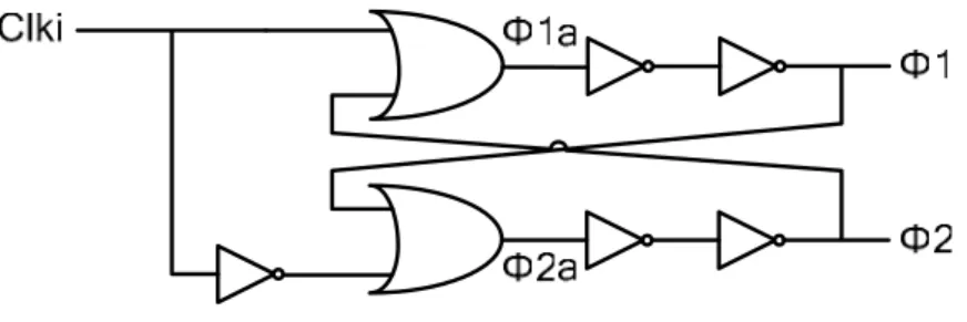
2.2.1 Clock generator
The clock signals could be generated by the scheme shows figure 2.1.
The nonoverlapping clock is essential in switched capacitor circuits. The two logic signal (Φ1,Φ2) would not both be high in the meanwhile. Φ1a andΦ2a are slighter than Φ1 and Φ2, respectively, for the purpose of alleviating charge injection error
[6] [11] and leakage.
Figure 2.1 Clock generator
2.2.2 Capacitor
The capacitor is largely used in analog CMOS circuit design. For capacitor design, several parameters are critical: nonlinearity, parasitic capacitor (accuracy) and density. Nonlinearity means the quiescent voltage dependence. The capacitor with less voltage dependency would contribute less harmonic distortion. Parasitic capacitor would affect the accuracy of the capacitor. In SC filter, it would make the corner frequency drift and gain vary. Density equals the capacitance per area by the capacitor. Large density can cost us smaller area to reach the desired capacitance.
Traditionally, a highly linear capacitance in an integrated circuit is constructed by two silicon area (double poly capacitors). The desired capacitor is formed by the intersection between two silicon layers. By growing a thin oxide between two conductive layers, it usually accompanies with 20% bottom plate parasitic capacitor.
The metal-insulator-metal (MIM) capacitor is often used in the modern analog circuits design. It is formed by two conductive mental layers and a PCB layer between them. It has a high density and a lower parasitic capacitance. The capacitance is defined by the intersection area and dielectric layer thickness. Under the threshold voltage, it can isolate the DC signal to hold the charge energy. In recent years, many researches about MIM capacitor focus on developing a high dielectric constant material [6].
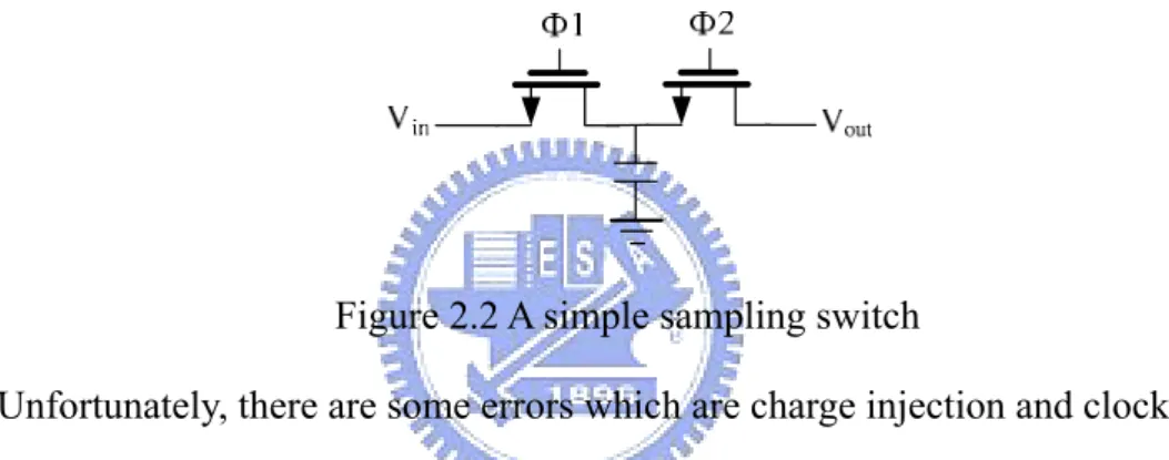
2.2.3 MOS sampling switch
In the common SC filter, we use single MOS transistor for sampling switch. It is shown in figure 4.2.For NMOS device, when the clock goes high, the transistor would be turn on and the output signal would track the input signal. It is assumed that the voltage of the capacitor equals zero initially. The transistor works in saturation region under the condition Vds >Vgs – Vt. Until Vds< Vgs-Vt, the transistor would enter the triode region. It would be stable in deep triode region when output signal nearly equals input signal. Thus it would result in a simple sampling switch with a high accuracy.
Figure 2.2 A simple sampling switch
Unfortunately, there are some errors which are charge injection and clock feedthrough. As we know, the transistor must produce an inversion layer, as to as charge channel, into working. When the transistor is closed, the channel would disappear and the channel charge would be released out. The released charge would flow to drain and source. The charge on the capacitor would also be affected. The total channel charge is expressed byQch ≈WLCox(VDD −Vin −Vth). In the most case, the
channel charge is often assumed to be divided by drain and source. But the real mechanism is very complicated. Now the error by charge injection equals
H th in DD ox C V V V WLC V 2 ) ( − − =
∆ we can find large transistor size and smaller sampling
capacitor would produce larger error. Another error source is clock feedthrough. It is induced by gate-drain and gate-source overlap capacitance. Clock feedthrough would happen on the clock transition. When signal goes high, the overlap capacitance would
be charged to clock voltage (Vck). When the signal goes down, the charge saved by capacitance would be released. The sampled output voltage would be affected. The error can be represented by
H ox ox CK C WC WC V V + = ∆ [6] [7].
2.2.4 opamp
In most case, the analysis of SC circuit operation is based on ideal amplifier. It can simplify the analysis and make the SC circuit well understood. But in reality, the amplifier is usually most important component. The whole performance is often dominated by the amplifier design. The adequate amplifier design would make the SC filter successful. Now there are some merits about the amplifier performance would be discussed.
Gain is often first considered by the amplifier design. The gain determines the precision of the system applying a negative feedback amplifier. The larger gain is able to raise the accuracy of the SC filter. Besides, the high gain is also necessary to
suppress the harmonic distortion and result in a fast settling time. In the common case, the open loop gain typically ranges from 40dB to 80dB.
Unit gain bandwidth and phase margin would dominate the linear settling
behavior of the amplifier. Larger unit-gain bandwidth and phase margin can make the circuit stable quickly. There is a thumb rule that the unit gain bandwidth is often five times than clock frequency at a unit gain SC integrator and the amplifier is with 70 degrees.
Another factor would affect the settling time is slew rate. The clock rate and total capacitance would be limited by the slew rate. Insufficient slew rate would not transfer the charge from the capacitor to another. The less capacitance is often less accuracy.
amplifier is often loaded by pure capacitive loading. The larger impedance would reduce the unit-gain frequency. Thus the circuit may not be settled quickly [6].
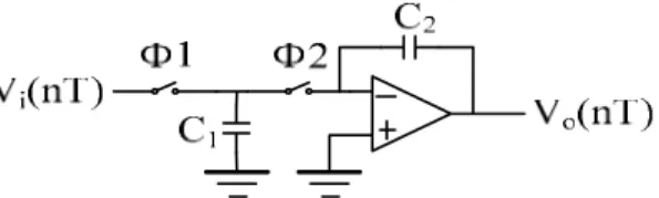
2.3 Switched capacitor integrator
The basic integrator is widely used in the SC circuit. A basic integrator is shown in figure 2.3the Φ1and Φ2 are nonoverlapped signal that means they are not turn on in the meanwhile.
Figure 2.3 A basic integrator
Assuming the integrator output voltage defined as Vout(nT-T) that means the charge on C2 equals C2Vout(nT-T). At the time (nT-T), SW1 is just turn off before SW is turn on. The charge on C1 equals C1Vin (nT-T). When SW2 is on, the charge on the C1 would be totally transferred to C2 because the negative input is virtually ground. Note that if a positive signal is applied on the input, it will result in a negative voltage on C2. The architecture is called inverting integrator. Thus we can find the charge equation at Φ2 end
2 co( / 2) 2 co( ) 1 ci( )
C V nT −T =C V nT −T −C V nT−T
We also can find the negative sign says that the integrator is an inverting
integrator. Like above, we also would like to derive the charge equation at Φ1 end. the charge on C2 at the end of the next Φ1 equals that at time (nT-T/2). It means that
2 co( ) 2 co(
C V nT =C V nT −T )
The charge equation can be expressed by
2 co( / 2) 2 co( ) 1 ci( )
C V nT −T =C V nT −T −C V nT−T
relationship. 1 2 ( ) ( 1) ( 1) o o i C V n V n V n C = − − −
Using the Z-transform,
1 1 1 2 ( ) ( ) ( ) o o C V Z Z V Z Z V Z C − − = − i
Now we can derive the transfer function
1 1 1 2 ( ) ( ) ( ) ( ) 1 o i V z C Z H Z V z C Z − − = − −
Unfortunately, as we mentioned before, the capacitors are often with parasitic
capacitance. In addition, the switches also have nonlinear capacitance. The figure 2.4 shows a basic integrator with parasitic capacitance. and represent the top and bottom capacitance of . and represent the top and bottom capacitance of . Because two ends of and connecting virtual ground node and ground node, respectively, there is little charge that would be stored. Thus their effects are often discarded. In addition, is just an extra loading for the amplifier. So it would affect the speed of the amplifier but not affect the accuracy of the output voltage. Finally, is parallel with . Then it would be also sampled signal like
. The sampled charge would be released on the next state and accuracy would be affected. To overcome this problem, the parasitic insensitive integrator is proposed [6] [8] [9]. 1 p C Cp2 1 C Cp3 Cp4 2 C Cp2 Cp3 4 p C 1 p C C1 1 C
Figure 2.4 The integrator with parasitic capacitors
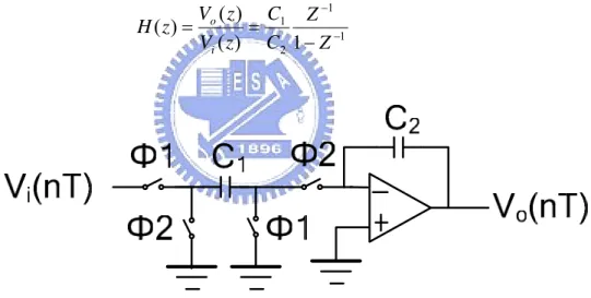
Parasitic insensitive integrator
Figure 2.5 shows a parasitic insensitive integrator. It can simply reduce the parasitic capacitance error by adding two extra switches. It has a difference from that we mentioned before which is a noninverting integrator. During 1φ , the capacitor C1 would sample the input signal Vi and the charge would be transferred to C2 on 2φ . We note the positive end of the capacitor is connected to ground node. This is why we called it is noniverting. When the input signal is positive, the opamp would contribute a positive signal on C2, with the phase as the same as input signal. Now we can find its transfer function as
1 1 2 1 1 ) ( ) ( ) ( − − − = = Z Z C C z V z V z H i o
Figure 2.5 A noniverting integrator
Now we add the parasitic capacitance for analyzing. As we noted before, only would affect the integrator accuracy. Now we can find would still sample the input signal on
1
p
C Cp1
1
φ , but it would be discharge to ground on 2φ . Unlike before, the switch with one end connected to ground would provide a path to ground for
discharging. The parasitic voltage would be charged to C2. It also would not affect the operation [6].
by changing the clock of the switches. The integrator is fundamental and important in the SC filter. It is essential to understand it completely.
Figure 2.6 An inverting integrator
2.4 Biquad Design [6]
There are many structures in the switched capacitor. The well-known one is biquad. Many complex filter is achieved by cascading the biquads. It is because the second biquad is often stable and realized easily. More flexibility for parameters is also why it is so popular. Before we introduce the biquad design, we often need the signal flow analysis. It is very useful in the biquad design. (Figure 2.7).
)
1
(
1
1 −− Z
C
Figure 2.7 Z-transformation signal flow
2.4.1 Low-Q biquad
The general transfer function of the continuous time biquad can be expressed by
2 0 0 2 0 1 2 ) ( w s Q w s d s d s d V V s H in out + + + + = = (2.1)
Then we can organize it into
out in s w Vin Q w V d s d s d V s2 =−( 2 2 + 1 + 0) −[( ) + 02] (2.2) Then we can find
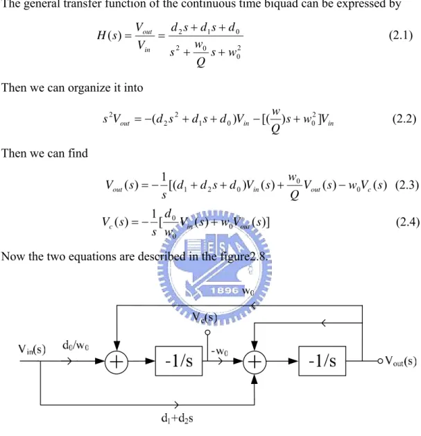
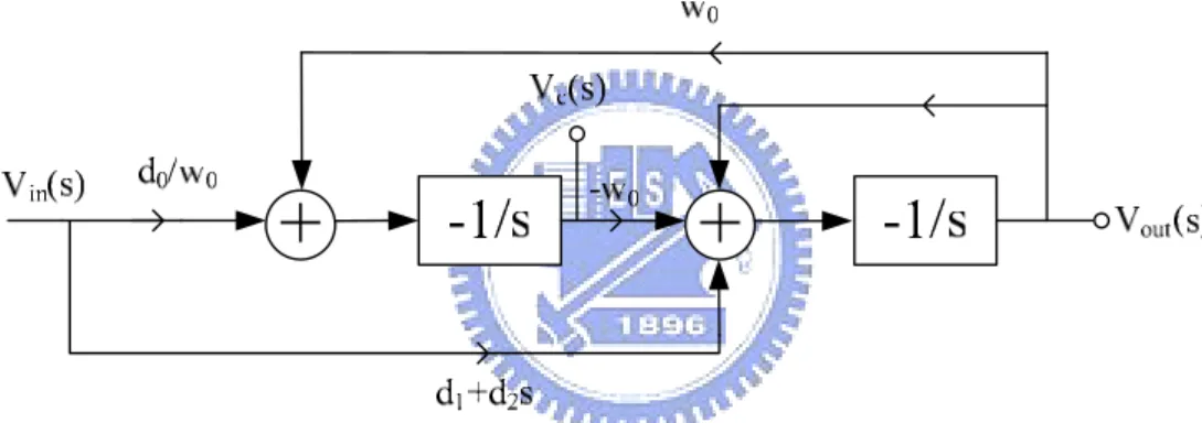
( ) 1[( ) ( ) 0 ( ) 0 ( ) 0 2 1 V s wV s Q w s V d s d d s s Vout =− + + in + out − c (2.3) ( ) 1[ ( ) 0 ( )] 0 0V s wV s w d s s Vc =− in + out (2.4) Now the two equations are described in the figure2.8.
Figure 2.8 Continuous time signal flow
Figure 2.9 A low Q RC continuous time RC filter
Finally, we substitute all resistors into the combination of switch and capacitor. The switched capacitor biquad is shown in figure 2.10.
Figure 2.10 A low-Q switched capacitor biquad
Using Z-transform signal flow analysis that we mentioned before, the transfer function is given by
1
)
2
(
)
1
(
)
2
(
)
(
)
(
6 5 4 2 6 3 3 2 5 1 2 3 2+
−
−
+
+
+
−
−
+
+
−
=
z
d
d
d
z
d
d
z
d
d
d
d
z
d
d
z
H
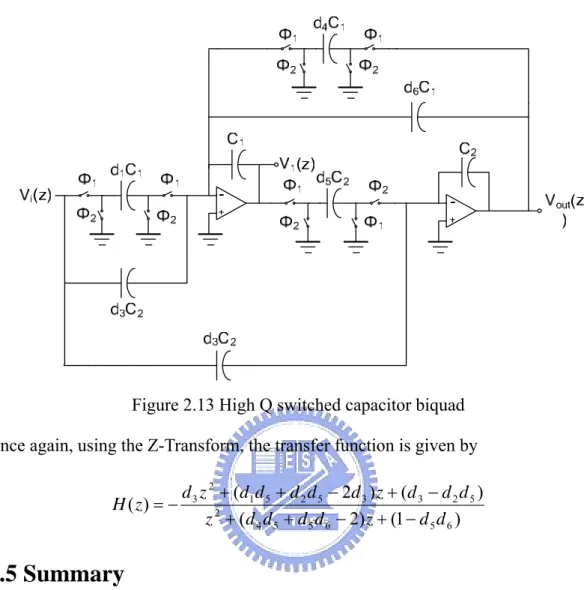
2.4.2 High-Q Biquad Filter
Using the same way, we also can complete a high Q circuit. We just reorganize equation (2.2) into )] ( ) ( [( 1 ) ( d2sV s w0V s s s Vout =− in − c and )] ( ) ( ) ( ) [( 1 ) ( 0 1 0 V s Q s s V w s V w s d w d s s Vc =− + in + out + out Now a new continuous time signal flow is obtained in figure 2.11
Figure 2.11 an alternative continuous time signal flow Like before, we also can derive a continuous time RC filter (figure 2.12)
We substitute all resistors into switches and capacitors. It is shown in Figure 2.13
Figure 2.13 High Q switched capacitor biquad Once again, using the Z-Transform, the transfer function is given by
) 1 ( ) 2 ( ) ( ) 2 ( ) ( 6 5 6 5 5 4 2 5 2 3 3 5 2 5 1 2 3 d d z d d d d z d d d z d d d d d z d z H − + − + + − + − + + − =
2.5 Summary
This chapter shows the common biquad design. In practice, we usually first
design a continuous time filter. Then it can be converted into discrete time filter or digital filter. The Z-transformation provides a concrete solution.
Chapter 3
High Performance Switched Capacitor
filter technique
3.1 Introduction
In this chapter, some modern circuit design techniques for high performance are illustrated. The characteristics of lower power supply, distortion and noise are all what we desired. Besides, in order to let the filter applied on communication system, we need to implement a wide band filter. Undoubtedly, the appropriate amplifier design is also very important, especially with a heavy loading. We will introduce what problems we may meet and their proposed solutions for pursuing high performance.
3.2 Low voltage SC circuit design
In analog circuit, dynamic range is often an important index to evaluate the analog circuit performance. In order to achieve high enough SNDR, a large signal swing range is necessary. But as we mentioned before, the signal swing of the MOS sampling switch would be restricted linearly by power supply. The low supply voltage would result in a smaller signal swing that makes dynamic range decrease and thus it is not expected. One solution for this is providing two power supplies, the higher one for the analog circuits and the lower one for the digital circuits. The disadvantage is needed a larger cost because we need to use different CMOS process. Thus there are several solutions in circuit design will be showed below [5].
3.2.1 Clock boosting
Clock boosting is a well known and straight forward approach to solve this problem. The reason for smaller signal swing is the reducing clock voltage. Thus we just boost our clock signal to enlarge the swing range.
The voltage doubler is often used [12] [13] [14]. (Figure 3.1) It is mainly formed by two N-type transistors, capacitors and an inverter. The cross-coupled transistors would alternatively be charged the capacitors to Vdd. Input clock is an ordinary periodic clock. After several periods, two capacitors would be both charged to Vdd. The output voltage of the inverter would be pumped a Vdd by C2. Now the ideal output signal would be 2Vdd. This cell is usually called “charge pump”. This idea is usually widely used in voltage boosting. When the input signal is high, M4 would discharge the gate of the sampling switch to ground. The output clock would be determined by G p DD H C C C C V V + + = 2 2 2 p
C is the parasitic capacitor of , and is the gate capacitance oh the MOS
sampling switch. But clock boosting often results in another problem that it would make the junction voltage exceed a Vdd. The junction breakdown issue is needed to be overcome especially in low threshold voltage process.
2 C CG H V DD V
3.2.2 Switch opamp technique
This is a method that allows the circuit operating in low voltage condition without any clock boosting [14] [15]. The system is really operating in low voltage without any junction breakdown problems. The basic concept is illustrated in
figure3.2 (a) shows the standard SC integrator. (b) shows an switch opamp integrator. The difference between two architectures is that switch opamp integrator operates without any floating sampling switch (S1). The original switch sampling function is
replaced by a switch opamp and a switch with one end connected to ground. Thus the signal swing would not be constrained by inefficient clock voltage. They can operate in 1V level with a typicalthreshold voltage that equals 0.7v. During
Φ
1
, the previous output is valid. The capacitor (C1) would be sampled the input signal. During , thecharge of C
2 Φ
1 would be transferred to C2, and node A would also be reset to ground. In
the meanwhile, the previous opamp would be switched off to avoid any conflict caused on the output. The opamp would be on or off alternatively. This is why it is called switch opamp. It overcomes the junction breakdown issue and benefits lower power. But the shortcoming of this architecture is much more complicated. It is not suitable for the analysis from the standard switched capacitor integrator. Besides it is often just used in low speed system because the opamp needs time to recover from “off” state to “on”state. With the comparison to standard switched capacitor circuit, it often has worse performance like linearity and noise.
(b) switched opamp integrator
3.2.3 Bootstrapped switch
Bootstrapped switch is a solution like clock boosting. The fundamental
operating concept is illustrated in figure 3.3. The sampling switch would be driven by a constant gate-source voltage. First the capacitor would be charged to Vdd. Then the input signal would be pumped by a Vdd. The gate voltage would be zero during “off“ state and Vsig+Vdd during “on” state, respectively. The turn-on resistance of a MOS switch is independent on input signal because of fixed Vgs and it would make the harmonic distortion decrease. But the high junction voltage may cause the breakdown. This technique is often with the reliability
Figure 3.3 Bootstrapped switch concept
3.2.4 A low voltage integrator design
For a SC filter, the problem what we meet is only signal swing that would be reduced by sampling switch. The signal amplitude is also restricted by the amplifier. Fortunately, we can solve this problem by adequate bias voltage. It is illustrated in
figure 3.4 means virtual ground, usually equaling to /2 and is the bias voltage making amplifier work properly. Assuming there is no input signal applied, the capacitor would have a voltage drop,
gnd
V VDD VB
gnd B V
V − , in the steady state. Since no net charge is transferred, also has the same voltage drop. If the integrator needs to work in low voltage, should be set close to for working properly. The output of the amplifier can be set to /2 to achieve maximum swing [16].
F C B V VDD DD V
V
inV
outV
BV
BC
FFigure 3.4 A low voltage integrator
3.2.5 Multi-threshold voltage process
Many advanced process would provide multi-threshold voltage device. The reason we need multi-threshold voltage is that, as we mentioned before, the analog circuit needs smaller threshold voltage for large signal swing. But the device with small threshold voltage would contribute larger leakage current. It would directly impact the digital circuit performance even result in failure. So the higher threshold voltage device is often used for digital circuits and the lower one is for analog circuits.
In addition, multi-threshold voltage process also means a larger cost [7].
3.3 Low distortion SC circuit design
3.3.1 Distortion mechanism
The distortion may be caused by any component in switched capacitor circuit. Before we introduce the design technique for low distortion switched capacitor circuit, it is essential to understand the distortion how to be generated [17].
A. Capacitor Nonlinearity
We often discuss the distortion in an integrator. This is because SC circuit seldom uses an amplifier without negative feedback. A single-ended SC integrator is shown in figure 3.5. The charge equation can be expressed by
) ( ] ) 2 1 [( ) 2 1 [( 2 0 1 1 2v n Tc C v n Tc Cv nTc C + − − =−
Now we use v0+,v0− and v1 to replace v n )T
2 1 [( 0 + , ) ] 2 1 [( 0 n Tc v − and v1(nTc) It would be Cv0+ −Cv0− =−Cv1 (3.1) We assume all nonideality is only contributed by the capacitor and other components are ideal. The capacitor voltage can be represented by
where Vc is the nominal values at quiescent voltage. In the most cases, we often just take the first two items into consideration and others would be ignored. The expression would be changed into the following
. We substitute it into equation 3.1
) 1 ( ) (Vc =Ci0 + 1Vc + 2Vc2 +" C α α ) 1 ( ) (Vc Ci0 1Vc 2Vc2 C = +α +α
The equation would be approximated by
]} ) ( ) ( [ ) ( { 1 1 1 1 0 0 2 1 12 0 2 0 0 0 2 20 10 0 0 − − + + − + − + − ≈− − − + + − − + + + v v v v v v v v v v v C C v v α α
Now we find the following relation
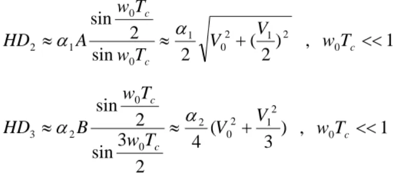
c nT w V v1 = 1cos 0 c c l c w n T T w V C C T n w V v ) 2 1 ( sin 2 sin 2 ) 2 1 ( cos 0 0 20 10 0 1 0 = ± =− ± ± ] ) 3 cos( ) 2 cos( [cos 0 1 0 2 2 0 3 1 20 10 0 0 − ≈− +"+ + +"+ + +" − + α θ α θ c c c A w nT B w nT nT w V C C v v
A, B are amplitudes and θ2,θ3 are phase.
2 1 2 0 1 0 0 1 2 ) 2 ( 2 sin 2 sin V V T w T w A HD c c + ≈ ≈α α , w0Tc <<1 ) 3 ( 4 2 3 sin 2 sin 2 1 2 0 2 0 0 2 3 V V T w T w B HD c c + ≈ ≈α α , w0Tc <<1
We can find the second and the third harmonic distortion are proportional to the output voltage and its square, respectively.
(a)
(b)
Figure 3.5 (a) Single-ended SC integrator (b) Two-phase clock B. Distortion caused by amplifier gain nonlinearity
The real opamp usually has finite gain and introduces the distortion into the SC circuit. We also take the integrator with a feedback factor which equals β into the
consideration. As the same as before, we assume all nonlinearity only comes from the amplifier and is caused by finite gain characteristic. The output voltage can be
" + + + = 3 1 2 1 2 1 1v a v av a
vo For simplicity, it would be approximated the first three
terms. As before, we can get the charge balance equation as follows
)] ( ) [( 1 0 1 0 1 1 1 1 − − + + + + − − − =Cv C v v v v v C
Now we can derive the approximation.
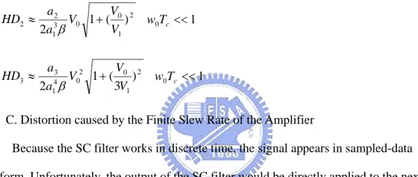
]} ) ( ] ) ( ) )( ( ) [( [ ] ) ( ) ( [ ) 1 1 {( 4 1 0 2 0 0 0 2 0 3 1 3 2 0 0 0 1 3 1 2 1 1 2 1 0 0 + − − + + + − + − + − ≈− + − + − − + + − v v v v v v a a v v v v a a v a C C v v β β β
In the expression, the second and the third term represent the errors.
2 1 0 0 3 1 2 2 1 ( ) 2 V V V a a HD ≈ + β w0Tc <<1 2 1 0 2 0 4 1 3 3 ) 3 ( 1 2 V V V a a HD ≈ + β w0Tc <<1
C. Distortion caused by the Finite Slew Rate of the Amplifier Because the SC filter works in discrete time, the signal appears in sampled-data
form. Unfortunately, the output of the SC filter would be directly applied to the next stage, as a continuous time system. The distortion would be caused by finite slew rate of the amplifier. To obtain the distortion caused by finite slew rate, we introduce a summarized model. (Figure 3.6).
x x y=
Figure 3.6 Model of slewing distortion
In this model, is the filter output and is the transition voltage. Transition voltage means the difference between current sampled output voltage and previous sampled voltage. The function
o
v x(t)
x x
assume the output sampled signal expressed by c o o o V w nT v = sin nT ≤t <(n+1)Tc Thus we can find x(t)
c c c c w n T T w V T n w V nT w V t x ) 2 1 ( cos 2 sin 2 ) 1 ( sin sin ) ( 0 0 0 0 0 0 0 − − = − = c c t n T nT ≤ <( +1)
Now we can find the transition voltage would be represented as a sampled cosine
) 1
wave with a varied magnitude and a shifted phase. The output of the distortion generator can be expressed by
) ( ' ) (t y nT y = c nTc ≤t <(n+ Tc t w t w T w y t V0 0 )2cos 0 cos 0 2 sin 2 ( ) ( ' = ) 4 ( ) 2 sin 2 ( 4 ) ( ' 2 2 0 0 − = k k T w V t y c π
From the model, the harm nic wave would be multiplied by an impulse stream a(t) o Thus the magnitude would be also multiplied by a factor
c rT S 2 1 The k th harmonic would be derived
c r c c T w V t y 0 0sin ) 2 ( 4 ) ( ' r r k T S V k k T w v k k T S V HD 0 2 2 0 0 2 0 ( 4) ) 2 (sin 8 1 ) 4 ( 2 2 1 − = − = = π π k =1,3,5,7,"
This equation shows that if slew rate is symmetrical, there are only odd harmonic
1 summarizes the distortion source [18]. present.
Table 3.1 Distortion Approximation
Distortion source THD theory
Capacitor Nonlinearity
Amplifier open-loop gain
Nonlinearity
Switch on resistance nonlinearity
Signal dependent charge injection of the switches
distortion caused by the finite slew rate of amplifier
3.3.2 The design consideration for l
ter
gn
techniq ,
aling if necessary.
ed. A. no
eans we need to scale the internal voltage of the SC filter
) 1 ( 2 2 2 2 ip op V V a + 3 16 Vop ) 2 2 Vop + Vop α 3 1 ( 16 3 0 Vip A β 2 2 1 2 16 2 ip on on V e e T ON s T τ τ − − 2 2 1 2 2 Ts T ON s τ ρ τ ρ + − SL T V T w s op s 2 0 ) 2 (sin 15 8 π
1
0T
s<<
w
ow distortion SC fil
From the above analysis of the distortion source, the low distortion desi ues would be illustrated in this section. To suppress the harmonic distortion there are three key points for designing.1. We must do internal voltage sc
2. Reducing internal components distortion 3. The differential architecture should be adopt de voltage scaling
Node voltage scaling m
properly. For lower distortion, the internal should be lower than the peak value of the passband. It can make the internal voltage would not be distorted before the output
voltage limits are reached. In another opinion, the smaller signal swing would result in much lower harmonic distortion. Thus we must try to keep internal signal smaller and the voltage only saturates at the output node.
B. Reducing internal components distortion
In ord filter, we need to design the
e
or the
ns.
fferential
Another
y would be a severe constraint. First, the
the er to lower the distortion generated within the SC
internal components carefully. The main components in the SC filter are switches, capacitors and amplifier. As we mentioned before last lection, we need try to depriv the filter of the distortion source. But the ideal component is impossible to be implemented. Thus we need to get a balance between all components design. F switch design, we need to suppress the distortion caused by turn-on resistance, charge injection and clock feedthrough. As to the distortion induced by the capacitor, we can adopt the differential architecture to mitigate them. For the amplifier design, it is essential to use the differential architecture. The even order distortion would be reduced and PSSRR would be raised. The signal swing also would be enlarged to resist the noise. Besides, we also need a high slew rate to alleviate the distortion caused by finite slew rate. We must pay more concentration on these circuit desig C. The differential architecture should be used
The harmonic distortion would be significantly reduced by fully di
architecture. The linear error and even order nonlinearity would be mitigated. advantage is a larger signal swing [17].
3.4 Summary
For the analog circuit, the low power suppl
signal swing would be reduced linearly. The sampling switch would not be driven properly. The integrator also meets the same problem. There are several solutions showed in this chapter. In order to design a low distortion filter, we also introduce
distortion mechanism and the design consideration. In the next chapter, we will use these techniques to realize a channel selection filter.
Chapter 4
A low voltage low distortion wide-band
CMOS switch capacitor filter
4.1 Introduction
The specification and architecture would dominate the distortion performance of the SC filter. The sampling period, corner frequency and nonideal device all would affect the THD of the output signal. The high sample rate can highly suppress the distortion, but it would be hard to implement an amplifier in this situation. Besides, in order to emerge the analog and digital circuits in the same power supply, the low voltage circuit design is unavoidable. It obviously makes the amplifier design more difficult. Even we can overcome this problem, the nonoverlapped high clock rate generation is also another key point.
In order to work out these problems, we must carefully choose the
architecture. Through a few architecture design consideration, we can complete a high speed low voltage filter immune to the distortion under the lower clock rate. Even using the same architecture, the bad setting of the parameters would be result in the lower performance. These are all what we need to take into consideration. Our filter architecture is made of a six-order elliptic filter. It is widely used in wireless receiver. In the direct conversion receiverthe receiving signal would be first filtered by a anti-aliasing low pass filter. The next, channel select filter, which we intend to carry out this time, would extract the signal band which we need. Finally, the last analog to digital converter would convert the filtering signal to digital code for the next digital
signal process (DSP).
Our channel select filter is composed of three serial second order biquad. As we say before, we adopted the SC filter. It works at 20M Hz with a cut off frequency at 2 MHz. We mainly choose the biquadratic filter because of its convenience. We can easily set all parameters and implement the whole circuit, especially in low voltage. It is a simple way to tune the filter and raise its performance.
In general, people often just focus its frequency response while designing filters, because it would make your filter design more simple. As to phase, we often use an equalizer behind the filter to take charge. Based on the first key point, we should avoid the internal signal magnitude close to the output signal maximum. It will
contribute more distortion because it would be limited by internal voltage level before the signal is restricted by the output terminal. The internal voltage boosting would result in large THD. We should do amplifying in the later stage. For the clock
feedthrough, it would be another source of THD. We can use the bottom sampling to solve it. In the meanwhile, using the differential architecture would suppress switch charge injection, clock feedthrough, even order distortion and linear capacitor voltage error.
Figure 4.1shows the all parameters of the channel select filter. Because the corner frequency locates on 2MHz, the bandwidth of the biquads should not exceed 2 MHz too far for free of high frequency harmonic distortion, or it would reduce the signal linearity. Besides, because the first stage is responsible for receiving signal, it often dominates the whole performance. So the first stage design is usually very important. In the first stage, the gain is set to be 0.8. This is what we said before about voltage scaling. The second stage would amplify the signal close to normal signal level. It is not considerate to do serial voltage scaling. If you do it, it means we need a
the output noise power raise. It is not what we want. If we would like to achieve a high dynamic range, we need to keep both medium distortion and noise. Another point needed to mention, the high Q stage is suitable in the later stage. But in practice, we may just do little under the constraint of the specification.It is hardly to meet all requirements. In the next section, we will discuss every building block to be used in our SC filter.
Figure 4.1 6th order elliptic filter parameters
4.2 Low voltage low distortion MOS sampling switch
Our novel MOS sampling switch is based on bootstrapped switch. Thus the bootstrapped switch and its modification would be explained in this section. A new MOS sampling switch is proposed in the end of this section.
Simple sampling Switch
Figure 4.2 shows a basic S/H circuit. When Ø is high (usually Vdd), the switch will be turned on and the capacitor will be charged to Vin. When Ø is low, the switch will be turned off and the capacitor will hold the sampled voltage. Its resistance is given by 1 ( ) n ox gs tn Ron W C V V L
µ
= − (4.1) where Vtn =Vt0+γ[ 2φF +VSB − 2φF ] (4.2)There are some obvious drawbacks in this sampling switch. The sampling switch output is limited to Vdd -Vt. If Vin > Vdd -Vt, the output voltage would be saturated and the incorrect voltage would be sampled. It would not have a full swing range. Besides, the resistance would vary with the input signal from Equation (4.1). It may donate larger harmonic distortion. The body effect also contributes nonlinearity, especially at low voltage. Therefore, the bootstrapped switch was proposed to solve the full swing problem and variation of the switch resistance.
BOOTSTRAPPED SWITCHES AND RELATED COMPENSATION
TECHNIQUES
From Equation (4.1), to obtain constant resistance, the gate to source voltage should be held constant during the “on” state.
Figure 4.3 The bootstrapped switch operation concept
Figure 4.3 shows the principle of the bootstrapped switch [19] and the circuit realization is shown in [20]. During the “off” state (SW3, SW4 and SW5 on), the capacitor would be charged to Vdd and likely act as a floating battery to bootstrap the gate voltage when the “on” state (SW1, SW2 on) . It is assumed the input terminal of the sampling switch would be source. Therefore, the resistance of the switch is given by 1 ( ) n ox t Ron W C Vdd V L µ = − (4.3)
Clearly, it can be independent of input signal to reduce harmonic distortion. However, the MOS switch is bidirectional and symmetric. The source and drain terminals may interchange depending on the input signal and previous sampled voltage. If the input signal is larger than previous sampled voltage, the source and drain terminal would be interchanged. Therefore, the source voltage is not Vin but sampled voltage in the previous state. Then, Vgs is not ”Vdd”. We can not maintain Vgs constant. Another distortion source of threshold voltage variation from body effect still dominate large distortion, especially in low power supply. Therefore, the body effect compensated switch was proposed in [22] [23]. The main idea behind [23] is to use direct connection from source to bulk to avoid the body effect during “on” state. This is a straightforward idea, but the real source is not always the input terminal in practice. And if the source of the P-type transistor is not highest voltage of all terminals, it may cause the latch-up problem [24]. Of course, Vsb also does not remain zero when the real source is not the input terminal of the sampling switch.
Another technique was proposed to use a replica transistor to cancel the threshold voltage [22], as shown in Figure 4.4. It is modified from a typical bootstrapped switch. It creates a threshold voltage as the same as the one sampling switch and cancel each other to be deprived of body effect. It is derived as follows. The drain current of MD in saturation is given by G
V
SV
DI
Figure 4.4 The replica compensation
2 1 ( ) 2 D n ox GS t W I C V V L µ = −
The drain current is constant by ignoring the second-order effect. Then we can find
1 ( ) 2 D G S t n o x I V V W C L µ = +
1 ( ) 2 D G t n o x I V V W C L µ = + +Vin d (4.4)
The gate voltage of the sampling switch would be equal toVG+Vd . Substituting Equation (4.4) into Equation (4.1) and assuming Vs equals Vi, Ron can be obtained as following. 1 2 ( ) ( ) D n ox dd n ox MD Ron I W C V W L C L µ µ = + (4.5)
From Equation (4.5), all the parameters of the resistance are constant, but this circuit still suffers from the problem described previously, where the source terminal might
be the input. In practice, the Vt of the sampling switch and replica would not match exactly due to the second order effect and process variation. It is difficult to be
compensated completely. The input signal is also needed to decrease by a threshold voltage to make sure the replica transistor in saturation. Another circuit was proposed
to modify this drawback of smaller swing range in [14].
The proposed sampling switch
Through the above discussion, a key point is that a “source follower” is needed to track the “real source” connecting the charged capacitor and maintaining
the gate overdrive to be a constant voltage ”Vdd”. Figure 4.5 shows the proposed circuit. The sampling switch is composed of a comparator and several switches.
Besides some necessary switches of a typical bootstrapped sampling switch, additional switches SW6 and SW7 are added. To ensure rail to rail swing, SW6 and
SW7 are made of complementary switches. The comparator is used to trigger SW6 and SW7 to make the bulk connect to the real source terminal. The bulk is guaranteed
to connect to only one terminal, the source terminal, during the “on” state. We adopt the structure of direct connection between source and bulk because it has less nonlinearity and large input swing than using a replica. In the standard CMOS technology, the sampling switch should be P-type. Two cases are discussed in the following where Vin represents input signal and Vout represents the voltage sampled in the “on” state.
Figure 4.5 The proposed sampling switch
Case 1: When Vin > Vout, the real source is the input terminal. During “off” state (SW2, SW3, and SW5 on), the capacitor would be charged to -Vdd. During the “on” state (SW1 and SW4 on), the comparator output will be low to turn on SW6 to make a connection between the input and bulk because input voltage is higher than
Vout . And the gate voltage of switch equals Vin - Vdd. Then the gate overdrive (Vsg) and Vsb exactly equals Vdd and zero respectively, during the “on” state.
source in V = V , Vgate =Vin−Vdd , Vtp =Vt0,Vsg =Vdd 0 1 ( ) p ox dd t Ron W C V V L µ = − (4.6)
Case 2: When Vin < Vout, the real source terminal should be the output terminal. It is certainly the reverse of case 1. The SW7 would be turn on by the comparator to connect the output and bulk. The gate voltage would become Vout - Vdd and the source voltage is also Vout. The gate overdrive (Vsg) still maintains exact Vdd. And threshold voltage is also held constant.
source out V =V ,Vgate =Vout −Vdd,Vtp =Vt0, Vsg =Vdd 0 1 ( ) p ox dd t Ron W C V V L µ = −
The above equation is the same as Equation (4.6). During “on” state, when the difference between input and output becomes “zero”, the comparator would be low and SW6 would be turn on again. At this time, we do not care which terminal is source because Vin already equals the sampled signal.
The power supply voltage is 1.8V. A 1.8Vpp 1Meg sinusoidal wave is applied to the ordinary bootstrapped switch without compensation, the bootstrapped switch with compensation in [22], and the proposed switch in this paper respectively. They are all loaded with 1 pF capacitance. The comparator in this paper has the voltage gain of 2000. Figure 4.6 illustrates the voltage of input, output, and bulk of
the sampling switch. It is shown that the bulk would track the lower signal between input and output.
Figure 4.7 shows the FFT of the output voltage in the ordinary bootstrapped switch without compensation, bootstrapped switch with compensation in [22], and the proposed switch in this paper. Table 4.1 summarizes the total distortion of these switches. The results show that total harmonic distortion (THD) is improved by 12.3dB and 42.5dB, respectively, in contrast to [22] and ordinary bootstrapped switch. The FFT results clearly indicate the huge improvement.
(a) Input signal
(b) Sampled signal
(c) Bulk signal
Figure 4.7 FFT of the switch output with small input signal
Table 4.1 Simulation results for harmonic distortion
Typical Ref[22] Proposed
THD -41.6db -71.8db -84.1db
HD2 -44.2db -72.7db -87.9db
The modified switch makes the rail to rail input signal possible for low voltage switched circuit. By desensitizing “on” resistance of the sampling switch, the linearity of switch is improved. The main idea is to distinguish which terminal is the real source terminal so that the gate overdrive voltage can be maintained exact Vdd and the variation of threshold voltage due to the body effect can be canceled for the analog switch. Because the bulk always connects to the real source, the latch-up problem would not exhibit. Finally, the ”on” resistance does not vary with the input signal and is immune to variation. The total harmonic distortion is highly suppressed.
4.3 Low Voltage Low distortion amplifier and integrator
It is important to design a good amplifier for switched capacitor circuit. The amplifier is the key component and its design would directly impact the whole performance. We should take it into more considerations. In low power supply, the transistors are not easily in deep saturation region. Therefore, the linearity of the amplifier would be much reduced. It is unavoidable. On the other hand, the non-ideal opamp would also contribute the distortion. The distortion usually results from finite gain, bandwidth and slew rate. These are also being taken into the consideration. The amplifier architecture applied for the switched capacitor filter is two-stage. The two stage amplifier can provide a large gain which can reduce the error caused by finite gain. The two-stage is also flexible for designing. Especially we need a large output current to improve the slew rate. Besides, we can benefit a low output resistance. The amplifier would not be much restricted by a large load. It is good to switched
capacitor filter because the large capacitor is often applied in it [25] [26]. For designing a high speed switched capacitor filter, setting time would be a critical point. Inadequate setting time would make the resolution of SC filter decrease, because the amplifier could hardly complete the charge or discharge on the capacitor.
Thus settling time would be a big impact on switched capacitor filter. For producing an adequate settling time, the bandwidth and slew rate of the amplifier should be taken into consideration. The infinite unit gain bandwidth and slew rate are both what we desired. But it is difficult to achieve. On the other hand, a high slew rate is
sometimes incompatible with a high gain. A high slew rate must be achieved by a large bias current in the output stage. It also may reduce the output resistance that makes the overall gain decline. We need to get a balance between them.
The settling time is highly related to the step response of the amplifier. It is often defined to the time which opamp can reach a specified percentage. The settling time consists of two distinct parts: non-linear and linear slewing. The linear portion is caused by finite unity-gain bandwidth of the amplifier. It would be a minimum value for the settling time. The non-linear segment is due to the slew rate limiting. So it is highly dependent on the output step size. In practice, the opamp with the negative feedback also acts like lowpass filter. It can reduce the high frequency harmonic distortion as well as the noise. Sometimes finite bandwidth also raises the linearity. Thus in our filter design, we adopted a two stage amplifier instead of a folded cascade. Especially it is easy to implement in low voltage. More flexible parameters can be used.
The main drawback is that the amplifier has a smaller bandwidth and common mode input range. The differential architecture can eliminate switch charge injection, clock feedthrough and even-order harmonic distortion. The linear error of the
capacitor is also alleviated. Besides, the signal swing and PSRR of the amplifier would be increased. In order to achieve a high signal swing, we need to set a common mode signal close to Vdd for N-mos input pair.
The two-stage amplifier is shown in Figure 4.8. The transistors M3 M4 M4C M5 M6 M6C provide the current mirrors. We can adjust the transconductance by
changing the transistor size ratios. M4-M8, M6C-M7C are the first gain stage. We use the self-bias structure for high stability. M9-M10 and M9C-M10C are the second stage. The circuit below the amplifier is common mode feedback circuit. It is formed by two differential pairs. In addition, for a large signal swing, the commode level should be close to Vdd instead of 1/2 Vdd with using N-input pair. In this case, we set it into 1V to get a large swing. We also enlarge the output current to raise the slew rate for low distortion, as we mentioned before. Figure 4.9 shows the frequency response of the amplifier (SS FF TT). The gain of the amplifier is about 78dB. High gain also helps us reduce the distortion caused by finite gain error. The unit-gain bandwidth of the amplifier is 100 MHz with 5p loading. Using the two-stage amplifier allows us to drive a large loading. The settling time about 11ns also meet our need. (Figure 4.11) Table 4.2 is the simulation result of the amplifier.
Figure 4.9 Frequency response of the amplifier
Figure 4.10 Settling time
Table 4.2 The simulation result of the amplifier
Amplifier Spec. Result
Process TSMC 0.18µm Mixed-Signal
Supply voltage 1.5v
Gain 78db
Cut-off frequency 100MHz
Slew rate 85v/us
Phase margin 87 degree
Settling time 11ns
Load 5p
Harmonic distortion -69.1dB@200k,1.2Vpp
4.4 The implementation of the filter
The biquad is shown infigure 4.11.This channel select filter is composed of three biquads. Table 4.3 shows the frequency response of the filter by SWITCAP. The passband attenuation is bout under 1dB within 2MHz. The signal frequency excess 2MHz would attenuate rapidly.
+ + -- + + -cm cm cm cm cm cm Vout1 Vout2 Vin1 Vin2 Ф2 Ф2 Ф2 Ф2 Ф2 Ф2 Ф2 Ф2 Ф2 Ф2 Ф2 Ф2 Ф2 Ф2 Ф2 Ф2 Ф1 Ф1 Ф1 Ф1 Ф1 Ф1 Ф1 Ф1 Ф1 Ф1 Ф1 Ф1 Ф1 Ф1 C1 C1 C2 C2 C3 C3 C4 C4 C5 C5 C7 C6 C6 C7
Table 4.3 Switcap simulation result (*): vdb(OUT) freq -60.00 -40.00 -20.00 .00 20.00 1.00-01 |---+---+---*---| 1.02-01 | * | ⇓ 1.90+06 | * | 1.94+06 | * | 1.97+06 | * | 2.01+06 | * | 2.05+06 | * | 2.09+06 | * | 2.12+06 | * | 2.16+06 | * | 2.20+06 | * | 2.25+06 | * | 2.29+06 | * | 2.33+06 | * | 2.37+06 | * | 2.42+06 | * | 2.46+06 | * | 2.51+06 | * | 2.56+06 | * | 2.60+06 | * | 2.65+06 | * | 2.70+06 | * | 2.75+06 | * | 2.80+06 | * | 2.85+06 | * | 2.91+06 | * | 2.96+06 | * | 3.02+06 | * | 3.07+06 | * | 3.13+06 | * | 3.19+06 | * | freq -60.00 -40.00 -20.00 .00 20.00 (*): vdb(OUT)