國 立 交 通 大 學
電子工程學系 電子研究所碩士班
碩 士 論 文
高介電係數金屬閘極平面式浮置閘極快閃記憶體特性
及其微縮模擬
Numerical Simulation of High-k/Metal Gate Floating Gate
Flash Memory Characteristics and Device Scaling
研 究 生 :房定樺
指導教授 :汪大暉 博士
高介電係數金屬閘極平面式浮置閘極快閃記憶體特性
及其元件微縮模擬
Numerical Simulation of High-k/Metal Gate Floating Gate
Flash Memory Characteristics and Device Scaling
研 究 生 : 房定樺 Student : Ding Hua, Fang
指導教授 : 汪大暉 博士 Advisor : Dr. Tahui Wang
國立交通大學
電子工程學系 電子研究所碩士班
碩士論文
A Thesis
Submitted to Department of Electronics Engineering and
Institute of Electronics
College of Electrical and Computer Engineering
National Chiao Tung University
in Partial Fulfillment of the Requirements
for the Degree of
Master of Science
in
Electronic Engineering
July 2012
Hsinchu, Taiwan, Republic of China.
i
高介電係數金屬閘極平面式浮置閘極快閃記憶
體特性及其微縮模擬
學生:房定樺
指導教授:汪大暉 博士
國立交通大學 電子工程學系 電子研究所
摘要
在本篇論文中,我們建立了一個模擬方法來模擬高介電係數金屬閘極 平面式浮置閘極快閃記憶體在寫入與消除的暫態行為,並使用 ISE TCAD 模擬軟體來模擬不同通道長度下操作時的電場分佈。我們模擬 有邊緣場效應與無邊緣場效應在通道長度為20奈米的平面式浮置閘極 快閃記憶體的寫入與消除操作下的比較,從我們模擬的結果可以得到邊緣 場效應會造成我們在寫入與消除操作效率變差,因此在平面式浮置閘極微 縮過程中,邊緣場效應扮演非常重要的角色。 為了在寫入與消除操作效率可以提高,我們必須改變其他高介電係數 材料當作阻擋層並模擬在不同阻擋層材料的寫入操作特性,我們也改變閘 極材料來模擬不同閘極材料在消除操作下的特性,由我們的模擬結果可以 發現用氧化鑭(La2O3)當作阻擋層可以有效地提高寫入與消除操作下 的效率。ii
Numerical Simulation of High-k/Metal Gate
Floating Gate Flash Memory Characteristics
and Device Scaling
Student: Ding Hua Fang Advisor: Dr. Tahui Wang
Department of Electronics Engineering &
Institute of Electronics
National Chiao Tung University
Abstract
In this dissertation a simulation method to simulate the transient behavior of
programming and erasing in high-k/metal gate planar floating gate flash memory is
developed. We also simulate the electric field distribution under different channel
length by ISE TCAD and compared the program/erase efficiency in channel length is
20 nm of planar floating gate flash memory with edge fringing field effect. From our
simulation result, the program/erase efficiency will be degraded by edge fringing
field effect. As a result, edge fringing field effect plays an important role in the
iii
To improve the program/erase efficiency, we have to simulate program
characteristics and change other high-k materials as blocking layer. We also simulated
erase characteristics under different gate material. From our simulation result,
lanthanum oxide as blocking layer could effectively promote program/erase efficiency
iv
Acknowledgement
首先,我要感謝我的指導教授汪大暉老師,老師教我做
研究嚴謹的態度,讓我在完成我的碩士論文過程中,很多小
細節都必須考慮清楚,沒有老師的嚴謹教誨,此論文根本就
不可能誕生,接下來我要感謝實驗室邱榮標和鍾岳庭學長,
邱榮標學長在我學習過程中,教我很多做研究的小技巧,讓
我在研究過程中受用不少,鍾岳庭學長在我完成我的碩士論
文過程中幫助我非常多,他也很不厭其煩的教我很多觀念及
做研究的技巧,讓我可以順利完成我的碩士論文,而我也要
感謝實驗室學弟學妹的加油打氣,讓我在受挫折的時候,又
有動力可以繼續做研究。
最後我要感謝我的父母及女朋友,他們在這段時間給我
精神上的支持及鼓勵,讓我可以順利完成我的碩士論文。
v
Contents
Chinese Abstract i English Abstract ii Acknowledgement Iv Contents v Figure Captions vi Chapter 1 Introduction 1Chapter 2 Floating Gate Numerical Simulation and Edge Effect 3
2.1 Introduction 3
2.2 Simulation Method 3
2.3 2.4
Program Characteristics due to edge effect Erase Characteristics due to edge effect
5
8
Chapter 3 Program/Erase Transient Behavior for High-k/Metal Gate Planar Floating Gate Flash Memory
26
3.1 Introduction 26
3.2 Program Characteristics for Different High-k Blocking Layer Materials
26
3.3 Erase Characteristics for Different High-k Blocking Layer and Gate Materials
27
Chapter 4 Conclusion 40
vi
Figure Captions
Fig. 2.1 Simulation method and flow chart of conventional FG flash memory.
p.10
Fig. 2.2 Simulation planar FG structure with stack SiO2/Poly-Si/Blocking
Layer is 7nm/120nm/7.5nm and channel length = 20nm, GCR=0.45.
p.11
Fig. 2.3 (a) Program and (b) erase characteristics for simulation result of conventional FG cell. Symbols are reported by [2.3] and lines are our simulation results.
P.12
Fig. 2.4 Electric field distribution in planar FG cell (a) without oxide spacer (b) with oxide spacer.
p.13
Fig. 2.5 Bottom potential drop ratio in Vg=15V verse (a) channel direction (b) channel length at x=0.
p.14
Fig. 2.6 Top potential drop ratio in Vg=15V verse (a) channel direction (b) channel length at x=0.
p.15
Fig. 2.7 Conduction energy band diagram at Vg=15V program operation, the Y-axis is from silicon substrate to gate.
p.16
Fig. 2.8 Conduction energy band diagram and electric field diagram in (a) bottom SiO2 (b) top HfO2.
p.17
Fig. 2.9 Correlation between effective electric field and channel length (a) bottom effective electric field (b) top effective electric field.
p.18
Fig. 2.10 Integration method of total FN tunneling current. p.19
vii
Fig. 2.12 Simulation result of program transient for planar FG with stack SiO2/Poly-Si/HfO2 is 7nm/100nm/13nm. Solid line with edge
effect and dash line are without edge effect.
p.21
Fig. 2.13 The Conduction energy band diagram at erase voltage = -15V bias, the Y-axis is from silicon substrate to gate.
p.22
Fig. 2.14 Conduction energy band diagram and electric field diagram in (a) bottom SiO2 (b) top HfO2.
p.23
Fig. 2.15 Correlation between effective electric field and channel length (a) bottom effective electric field (b) top effective electric field.
p.24
Fig. 2.16 Simulation result of erase transient for planar FG with stack SiO2/Poly-Si/HfO2 is 7nm/100nm/13nm. Solid line with edge
effect and dash line are without edge effect.
p.25
Fig. 3.1 (a) Compare ISPP slope under different high-k material as blocking layer at time is 10s.
(b) Compare top FN tunneling current under different high-k material as blocking layer.
p.30
Fig. 3.2 Compare the program capability under various gate voltage bias and high-k material as blocking layer.
p.31
Fig. 3.3 (a) Compare ISPE slope under different high-k material as blocking layer at time is 1ms.
(b) Compare top FN tunneling current under different high-k material as blocking layer.
p.32
Fig. 3.4 Simulated DVT at erase time = 1ms under various erase voltage bias for various B. SiO2/Poly-Si/La2O3 stack now is
7nm/100nm/13nm and several gate materials are also labeled.
p.33
Fig. 3.5 The correlation between top/bottom FN tunneling current and erasing time at erase voltage = -19V for (a) n+-poly gate (b) TaN metal gate.
viii
Fig. 3.6 The energy band diagram between lanthanum oxide and gate material at erase gate voltage bias applied under different gate material.
p.35
Fig. 3.7 Compare the erase capability under various gate bias and B. B
is the band offset between gate material and blocking layer.
p.36
Fig. 3.8 The planar FG structure of our simulation. p.37
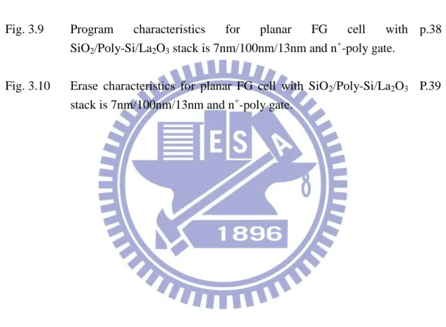
Fig. 3.9 Program characteristics for planar FG cell with SiO2/Poly-Si/La2O3 stack is 7nm/100nm/13nm and n+-poly gate.
p.38
Fig. 3.10 Erase characteristics for planar FG cell with SiO2/Poly-Si/La2O3
stack is 7nm/100nm/13nm and n+-poly gate.
1
Chapter 1
Introduction
Flash memory is the most widely used non-volatile information storage device
today, floating gate NAND flash memory device is the most aggressively scaled electronic device. In this work, we will discuss possible problems arising from
continued scaling of conventional FG structure and novel scaling issue.
Although floating gate NAND flash memory has scaled into 30nm node recently,
further scaling to 20nm may require using planar FG. Conventional FG is essential to decrease the floating gate height in order to limit cell to cell interference. However, it
can not be decreased when a large FG sidewall area is required for control gate coupling [1.1] [1.2]. Conventional floating gate flash memory scaling has been
researched recently[1.3] [1.4], consisting of floating gate structure and different high-k blocking layer and gate materials, however there are few research in planar
high-k metal/gate FG scaling issue [1.5] [1.6]. We will discuss program/erase efficiency due to edge fringing field effect [1.7] [1.8] when the planar FG scales into
20nm.
There are four chapters in this thesis. Chapter 1 is introduction and we will
introduce the conventional FG scaling issue and the conventional FG will be replaced by planar FG. In Chapter 2, we will introduce the simulation method and result of
conventional/planar floating gate flash memory in order to confirm our simulation method and discuss the oxide spacer induced edge fringing field effect in short
channel planar FG device. For this reason, the program/erase efficiency will degrade due to edge fringing field effect. In Chapter 3, we will discuss program/erase
characteristics for different high-k blocking layer and gate materials and combine
2
3
Chapter 2
Floating Gate Numerical Simulation
and Edge effect
2.1 Introduction
Floating gate flash memory with high-k blocking layer has recently received
much attention for the application in the next-generation nonvolatile memories because their better program/erase efficiency. Most research involves conventional
floating gate structure with high-k blocking layer materials, however our discussion is concerned with high-k/metal gate planar FG structure [1.5] and edge fringing field
effect [2.1] in short channel high-k/metal gate planar FG device.
First, to develop our simulation method for high-k/metal gate planar floating gate
flash memory, we have to verify between the experiment data and simulation is needed to confirm.
Second, based on the simulation method and flow we can simulate high-k/metal gate planar FG at different channel length. Furthermore, we will discuss the edge
fringing field effect at different channel length and explain the result of program/erase efficiency.
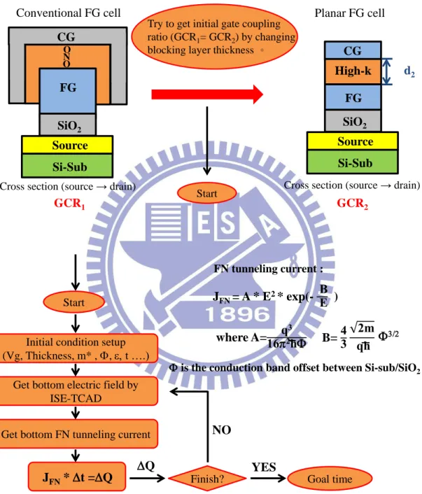
2.2 Simulation Method
Fig. 2.1 illustrates the simulation method and flow chart of conventional FG. The conventional FG structure is immensely complex. For simplification, we have to
simplify the structure. We can ignore top tunneling current in conventional FG due to relatively gate coupling ratio (GCR1) [2.2]. Due to these key points, we proposed a
4
the planar FG is equivalent to conventional FG because they have the same initial gate
coupling ratio. Therefore, we try to get the initial gate coupling ratio (GCR1=GCR2)
by changing blocking layer thickness, which method could promote our simulation.
First, to get bottom electric field from ISE TCAD, we must give critical parameters and initial condition in ISE TCAD. The tunneling current is selected by
the bottom oxide electric field due to ignore the top tunneling current. The tunneling current mechanism is FN tunneling. The tunneling barrier determined by the
conduction band offset between silicon substrate and bottom oxide, the current is from FN tunneling.
Second, based on the FN tunneling current (JFN) we can get amount of charge Q
from following Eq. (2.1):
Eq. (2.1)
t is time of initial condition.
Finally, the simulation process will stop at our goal time.
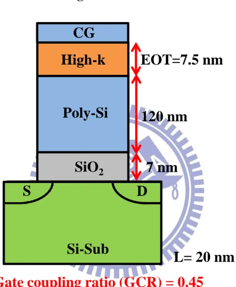
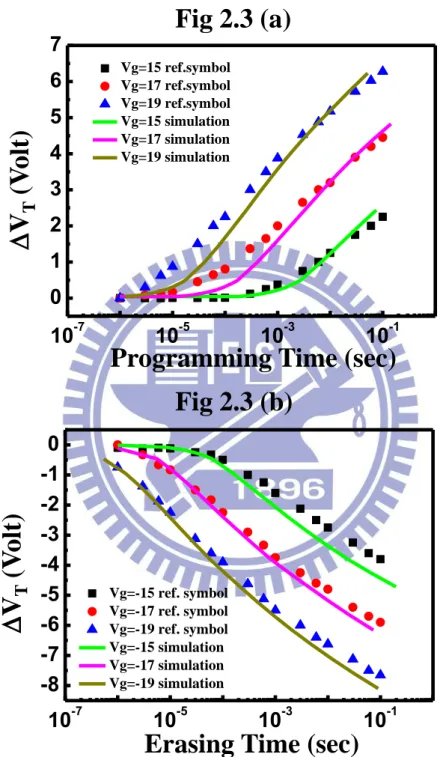
To confirm the simulation method established above, we choice an ideal material
as blocking layer in order to ignore top FN tunneling current. The planar FG with stack is SiO2/Poly-Si/Blocking Layer is 7nm/120nm/7.5nm and gate coupling ratio =
0.45 as show in Fig. 2.2. The simulation planar FG structure and the reference of
conventional FG structure with the same initial gate coupling ratio. JFN * t =Q
5
As a result of same GCR, the simulation planar FG is equivalent to the reference
conventional FG. In Fig. 2.3, the data of the reference [2.3] is quoted and our simulations fit both on its program and erase behaviors well.
2.3 Program Characteristics due to Edge Effect
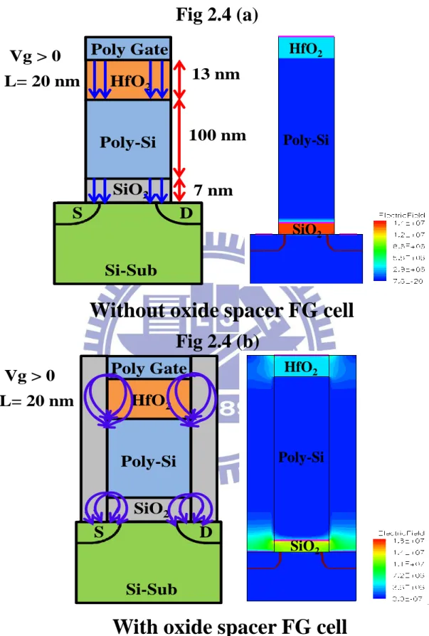
Fig. 2.4 illustrates the electric field distribution in planar FG with/without oxide
spacer and the stack is SiO2/Poly-Si/HfO2 is 7nm/100nm/13nm, channel length is
20nm. From Fig. 2.4 (a), the top blocking layer and bottom oxide electric field are
uniform distribution in planar FG without oxide spacer. However, from Fig. 2.4 (b), the top blocking layer and bottom oxide electric field are non-uniform distribution due
to the top and bottom edge fringing field effect. Therefore, the planar FG with oxide spacer must be taken account of edge fringing field effect [2.1] in short channel planar
FG device.
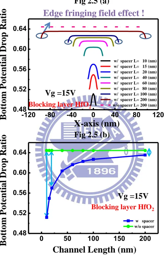
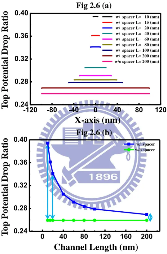
According to the simulation result illustrated in Fig. 2.5 (a) and (b), the bottom
potential drop ratio is decreasing in short channel planar FG device due to edge effect in short channel planar FG device is more serious than long channel planar FG device.
Therefore, we can predict the program/erase efficiency will degrade in short channel planar FG device due to the bottom electric field becomes weaker than long channel
planar FG. Fig. 2.6 illustrates the correlation between top potential drop ratio and channel length. From Fig. 2.6 (a), the top potential drop ratio increases with channel
length due to edge effect in short channel planar FG device is also more serious than long channel planar FG device. Therefore, we can also predict the program/erase
efficiency will degrade in short channel planar FG device due to the top FN tunneling current will tunnel out easily from control gate.
6
Based on the above discussion, we can make our conclusion that program/erase
efficiency will be degraded by edge fringing field effect in short channel planar FG device.
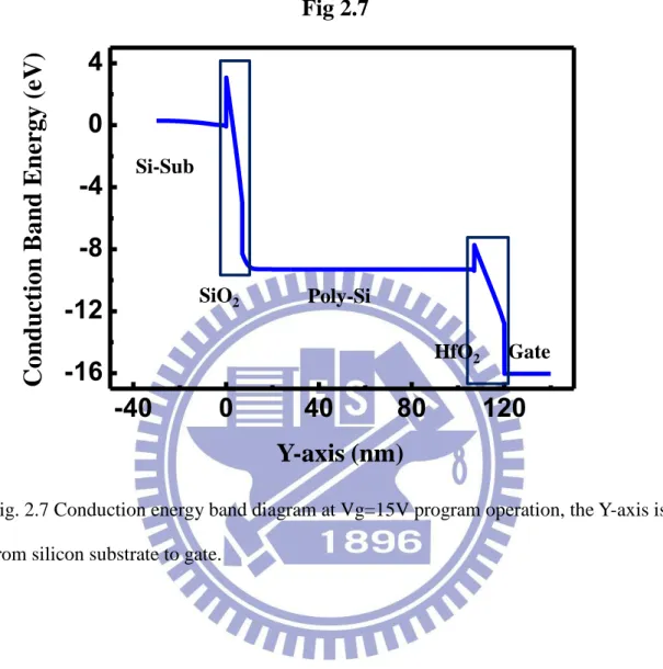
Due to edge fringing field effect, both top and bottom electric field are non-uniform distribution. As a result, we have to calculate effective electric field in
program/erase operation. The method of calculate effective electric field as show in Fig.2.7. Fig 2.7 (a) illustrates the conduction energy band diagram at program
operation, and we focus on bottom silicon dioxide and top hafnium oxide. The conduction energy band diagram of bottom silicon dioxide as show in Fig. 2.7 (b).
The FN tunneling current will tunnel from substrate to polysilicon at programming, therefore, the FN tunneling current has to tunnel through a barrier. The barrier is not
the whole of the area of tunneling but the top small area of tunneling. We can receive
the tunneling distance Y1 by ISE TCAD, and the FN tunneling current will not pass
through the large electric field region. The large electric field region is located within the interface of SiO2/poly-Si. Therefore we have to calculate the effective electric
field from following Eq. (2.2)
Eq. (2.2)
Fig. 2.7 (c). is the conduction energy band diagram of top hafnium oxide. The FN tunneling current will tunnel to top hafnium oxide from polysilicon and tunnel
through a barrier. The barrier is also not the whole of the area of tunneling but the top
small area of tunneling. The Y2 is tunneling distances, we can also calculate the
effective electric field in top hafnium oxide for the same way.
7
As the result of Eq. (2.2), the bottom and top effective electric field show in
Fig.2.8, and a shorter channel length denoted the edge fringing field effect is larger. From Fig. 2.8 (a), we compared the bottom effective electric field with different
channel length at gate voltage is 15V, and a dimensional dependence of edge fringing field effect is investigated, which a smaller device demonstrated a larger edge effect.
The effective electric field of bottom oxide is decreasing in short channel planar FG, the program/erase efficiency will be degraded by this phenomenon. Fig. 2.8 (b)
illustrates the correlation between top effective electric field and channel length, the edge fringing field effect is severe in short channel planar FG device. The effective
electric field of top hafnium oxide increases with channel length, which induced the FN tunneling current will easily tunnel out from control gate. Therefore,
program/erase efficiency will also be degraded by edge fringing field effect in short channel planar FG device.
Based on the above discussion, both top and bottom electric field are non-uniform distribution due to edge fringing field effect. This phenomenon is severe
in short channel device, therefore, we have to integrate total FN tunneling current. The integration of total FN tunneling current as show in Fig. 2.9.
Fig. 2.10 illustrates the simulation flow chart of planar FG. The simulation flow chart difference between conventional is that we have to calculate effective electric
field and integrate total FN tunneling current in planar FG simulation flow. Based on the simulation flow chart, we can simulate the program transient for planar FG with
SiO2/Poly-si/HfO2 stack is 7nm/10nm/12nm, channel length is 20nm. The simulation
result as show in Fig 2.11. From Fig 2.11, the program window and program speed
8
2.4 Erase Characteristics due to Edge Effect
In previous section, we discussed the correlation between effective electric field
with different channel length in programming. In this section, we dicuss the correlation between different channel length and effective electric field in erasing.
Similarly, we have to calculate effective electric field in erase operation. The method of calculate effective electric field as show in Fig.2.12. Fig 2.12 (a) illustrates
the conduction energy band diagram at erase operation, and we focus on bottom silicon dioxide and top hafnium oxide. From Fig. 2.12 (b), the conduction energy
band diagram shows in bottom silicon dioxide. The FN tunneling current will tunnel to substrate from polysilicon at erasing, therefore, the FN tunneling current has to
tunnel through a barrier. The barrier is also not the whole of the are of tunneling but
the top small area of tunneling. We can receive the tunneling distance Y1 by ISE
TCAD, and the FN tunneling current will pass through the large electric field region. The large electric field region is located within the interface of SiO2/poly-Si.
Therefore we also have to calculate the effective electric field from Eq. (2.2).
Fig. 2.12 (c) is the conduction energy band diagram of top hafnium oxide. The
FN tunneling current will tunnel to polysilicon from top hafnium oxide and tunnel through a barrier. The barrier is also the whole of the area of tunneling but the top
small area of tunneling. The Y2 is tunneling distances, we can also calculate the
effective electric field in top hafnium oxide for the same way.
As the result of the above discussion, the bottom and top effective electric field show in Fig.2.13, a shorter channel length denoted the edge fringing field effect is
larger. From Fig. 2.13 (a), we compared the bottom effective electric field with different channel length at gate voltage is -15V, a dimensional dependence of edge
9
edge effect. The bottom effective electric field decreases with channel length, the
erase efficiency will be degraded by this phenomenon due to the FN tunneling current easily tunnel out from floating gate to substrate. Fig. 2.13 (b) illustrates the correlation
between top effective electric field and channel length, and the edge fringing field effect is also severe in short channel planar FG device. The top effective electric field
increases with channel length, which induced the gate injection current will easily tunnel in from gate. Therefore, erase efficiency will also be degraded by edge fringing
field effect in short channel planar FG device.
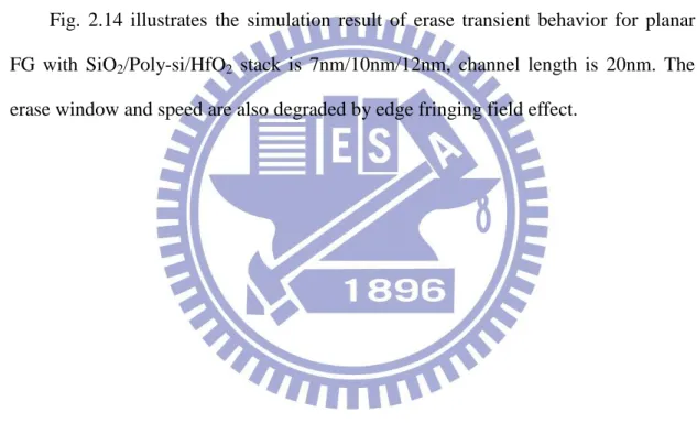
Fig. 2.14 illustrates the simulation result of erase transient behavior for planar
FG with SiO2/Poly-si/HfO2 stack is 7nm/10nm/12nm, channel length is 20nm. The
10
Fig. 2.1 Simulation Method and flow chart of conventional FG flash memory. .
Planar FG cell
GCR1 GCR2
Try to get initial gate coupling ratio (GCR1= GCR2) by changing blocking layer thickness 。
Start SiO2 FG CG d2 Si-Sub Source
Cross section (source → drain)
High-k Fig 2.1
Conventional FG cell
Cross section (source → drain)
SiO2 FG Si-Sub Source CG O N O Q Start
Initial condition setup (Vg, Thickness, m* , , e, t ….)
Get bottom electric field by ISE-TCAD
JFN* t =Q
Get bottom FN tunneling current
Finish? Goal time
NO YES where A= JFN = A * E2 * exp(- ) B= 3/2 FN tunneling current :
11
Fig. 2.2 Simulation planar FG structure with stack SiO2/Poly-Si/Blocking Layer is
7nm/120nm/7.5nm and channel length = 20nm, GCR=0.45.
Fig 2.2
Gate coupling ratio (GCR) = 0.45
120 nm
7 nm
EOT=7.5 nm
SiO
2Poly-Si
S
D
Si-Sub
CG
High-k
L= 20 nm
12
Fig. 2.3 (a) Program and (b) erase characteristics for simulation results of
conventional FG cell. Symbols are reported by [2.3] and lines are our simulation
results.
10
-710
-510
-310
-10
1
2
3
4
5
6
7
Vg=15 ref.symbol Vg=17 ref.symbol Vg=19 ref.symbol Vg=15 simulation Vg=17 simulation Vg=19 simulationProgramming Time (sec)
V
T(V
olt)
10
-710
-510
-310
-1-8
-7
-6
-5
-4
-3
-2
-1
0
Vg=-15 ref. symbol Vg=-17 ref. symbol Vg=-19 ref. symbol Vg=-15 simulation Vg=-17 simulation Vg=-19 simulationErasing Time (sec)
V
T(V
ol
t)
Fig 2.3 (a)
Fig 2.3 (b)
13
Fig. 2.4 Electric field distribution in planar FG cell (a) without oxide spacer (b) with
oxide spacer
Without oxide spacer FG cell
HfO
2SiO
2Poly-Si
S
D
Si-Sub
Poly Gate
Vg > 0
100 nm
7 nm
13 nm
L= 20 nm
Poly-Si
SiO
2HfO
2With oxide spacer FG cell
HfO
2SiO
2Poly-Si
S
D
Si-Sub
Poly Gate
Vg > 0
L= 20 nm
Poly-Si
SiO
2HfO
2Fig 2.4 (a)
Fig 2.4 (b)
14
Fig. 2.5 Bottom potential drop ratio in Vg=15V verse (a) channel direction (b)
channel length at x=0.
Fig 2.5 (a)
Fig 2.5 (b)
X-axis (nm)
Bott
om
Pot
entia
l
Dr
op
Ra
tio
Vg =15V
Blocking layer HfO
2Bot
to
m
Po
ten
tia
l
Dr
o
p
Ra
tio
Channel Length (nm)
Blocking layer HfO
2Vg =15V
Edge fringing field effect !
-120
-80
-40
0
40
80
120
0.48
0.52
0.56
0.60
0.64
w/ spacer L= 10 (nm) w/ spacer L= 15 (nm) w/ spacer L= 20 (nm) w/ spacer L= 40 (nm) w/ spacer L= 60 (nm) w/ spacer L= 80 (nm) w/ spacer L= 100 (nm) w/ spacer L= 200 (nm) w/o spacer L= 200 (nm)0
50
100
150
200
0.48
0.52
0.56
0.60
0.64
w spacer w/o spacer15
Fig. 2.6 Top potential drop ratio in Vg=15V verse (a) channel direction (b) channel
length at x=0.
Fig 2.6 (a)
Fig 2.6 (b)
X-axis (nm)
T
op
Pot
ential
Dr
op
Ra
tio
T
op
Pot
ential
Dr
op
Ra
tio
Channel Length (nm)
-120
-80
-40
0
40
80
120
0.24
0.28
0.32
0.36
0.40
w/ spacer L= 10 (nm) w/ spacer L= 15 (nm) w/ spacer L= 20 (nm) w/ spacer L= 40 (nm) w/ spacer L= 60 (nm) w/ spacer L= 80 (nm) w/ spacer L= 100 (nm) w/ spacer L= 200 (nm) w/o spacer L= 200 (nm)0
40
80
120
160
200
0.24
0.28
0.32
0.36
0.40
w/ spacer w/o spacer16
Fig. 2.7 Conduction energy band diagram at Vg=15V program operation, the Y-axis is
from silicon substrate to gate.
-40
0
40
80
120
-16
-12
-8
-4
0
4
Y-axis (nm)
C
o
nd
uct
ion
Ba
nd
Energ
y
(
eV
)
Poly-Si SiO2 Si-Sub HfO2 GateFig 2.7
17
Fig. 2.8 Conduction energy band diagram and electric field diagram in (a) bottom SiO2 (b) top HfO2.
0 5 10 15 -10 -5 0 5 105 110 115 120 -20 -15 -10 -5 Co ndu ct io n Ba nd Ene rg y ( eV ) Co ndu cti o n Ba nd Ene rg y ( eV ) Y-axis (nm) Y-axis (nm) Gate Si-Sub SiO2 Poly-Si HfO2 Y1 VA VB Y2 VB VA Y1 Y2
Y-axis
HfO
2SiO
2Y-axis
Programming
Fig 2.8 (a)
Fig 2.8 (b)
18
Fig. 2.9 Correlation between effective electric field and channel length (a) bottom effective electric field (b) top effective electric field.
T
op
E
ef fe ctive(10
6V/cm
)
Bottom
E
ef fe ctive(10
6V/cm
)
X-axis (nm)
X-axis (nm)
Vg =15V
Blocking layer HfO2
Vg =15V
Blocking layer HfO2
Fig 2.9 (a)
Fig 2.9 (b)
Edge fringing field effect !
-60
-40
-20
0
20
40
60
9
10
11
12
13
14
w/ spacer L= 10 (nm) w/ spacer L= 15 (nm) w/ spacer L= 20 (nm) w/ spacer L= 40 (nm) w/ spacer L= 80 (nm) w/ spacer L=100 (nm) w/o spacer L=100 (nm)-60
-40
-20
0
20
40
60
2.8
3.2
3.6
4.0
4.4
w/ spacer L= 10 (nm) w/ spacer L= 15 (nm) w/ spacer L= 20 (nm) w/ spacer L= 40 (nm) w/ spacer L= 80 (nm) w/ spacer L=100 (nm) w/o spacer L=100 (nm)19
Fig. 2.10 Integration method of total FN tunneling current.
High-k
SiO
2FG
S
D
Si-Sub
CG
Vg > 0
X
J =
J
1J
2J
3……….
J
nJ
1*
X
1+J
2*
X
2+…...+J
n*
X
n
X
1+
X
2+…...+
X
n=
J
1*
X
1+J
2*
X
2+…...+J
n*
X
nL
Integration of FN tunneling current :
L : channel length
Si-Sub
SiO
2X1X2X3
……….
Xn20
Fig. 2.11 Simulation flow chart of program /erase transient for planar FG. Q
(J1=J2)
Start
Initial condition setup (Vg, Thickness, m* , , e, t ….)
Get effective electric field by ISE-TCAD
JFN* t =Q
Integrate total top and bottom FN tunneling current Finish? End NO YES High-k SiO2 FG S D Si-Sub CG High-k SiO2 FG S D Si-Sub CG Vg > 0 Vg < 0 J1 J2 J1 J2 Fig 2.11
21
Fig. 2.12 Simulation result of program transient for planar FG with stack
SiO2/Poly-Si/HfO2 is 7nm/100nm/13nm. Solid line with edge effect and dash line are
without edge effect.
10
-710
-610
-510
-410
-310
-210
-110
0-4
-2
0
2
4
6
Vg=14 w/o spacer Vg=15 w/o spacer Vg=16 w/o spacer Vg=17 w/o spacer Vg=14 w/ spacer Vg=15 w/ spacer Vg=16 w/ spacer Vg=17 w/ spacerProgramming Time (sec)
V
T=
V
T-V
T i ni tia l(V
olt)
Blocking layer HfO
2with fringing effect !
without fringing effect !
Fig 2.12
22
Fig. 2.13 The Conduction energy band diagram at erase voltage = -15V bias, the Y-axis is from silicon substrate to gate.
-40
0
40
80
120
160
0
4
8
12
16
Y-axis (nm)
Co
nduct
ion
Band E
nergy
(
eV
)
Poly-Si SiO2 Si-Sub HfO2 GateFig 2.13
23
Fig. 2.14 Conduction energy band diagram and TCAD electric field plot in (a) bottom SiO2 (b) top HfO2.
0 5 10 15 0 5 10 15 105 110 115 120 5 10 15 20 C o nducti o n Ba nd Energ y ( eV ) Y-axis (nm) Co ndu cti o n Ba nd Ene rg y ( eV ) Y-axis (nm) Si-Sub SiO2 Poly-Si Gate HfO2
Erasing
Y1 Y2Y-axis
HfO
2SiO
2Y-axis
Y1 VA VB Y2 VA VBFig 2.14 (a)
Fig 2.14 (b)
24
Fig. 2.15 Correlation between effective electric field and channel length (a) bottom oxide effective electric field (b) top hafnium effective electric field.
T
op
E
ef fe ctive(10
6V/cm
)
Bottom
E
ef fe ct ive(10
6V/cm)
X-axis (nm)
X-axis (nm)
Edge fringing field effect !
Fig 2.15 (a)
Fig 2.15 (b)
-60
-40
-20
0
20
40
60
12
14
16
18
w/ spacer L= 10 (nm) w/ spacer L= 15 (nm) w/ spacer L= 20 (nm) w/ spacer L= 40 (nm) w/ spacer L= 80 (nm) w/ spacer L=100 (nm) w/o spacer L=100 (nm)-60
-40
-20
0
20
40
60
2.8
3.2
3.6
4.0
4.4
4.8
5.2
w/ spacer L= 10 (nm) w/ spacer L= 15 (nm) w/ spacer L= 20 (nm) w/ spacer L= 40 (nm) w/ spacer L= 80 (nm) w/ spacer L=100 (nm) w/o spacer L=100 (nm)25
Fig. 2.16 Simulation result of erase transient for planar FG with stack
SiO2/Poly-Si/HfO2 is 7nm/100nm/13nm. Solid line with edge effect and dash line are
without edge effect.
10
-710
-610
-510
-410
-310
-210
-110
0-6
-5
-4
-3
-2
-1
0
1
2
3
4
Vg=-14 w/ spacer Vg=-15 w/ spacer Vg=-16 w/ spacer Vg=-17 w/ spacer Vg=-14 w/o spacer Vg=-15 w/o spacer Vg=-16 w/o spacer Vg=-17 w/o spacerErasing Time (sec)
V
T=
V
T-V
T i ni tia l(V
olt)
Blocking layer HfO
2with fringing effect !
Without fringing effect !
L= 20 nm
26
Chapter 3
Program/Erase Transient Behaviors for
High-k/Metal Gate Floating Gate Flash Memory
3.1 Introduction
In planar FG with conventional ONO stack as blocking layer, the program/erase efficiency is poor as show in [2.1]. As a result, the conventional ONO stack will be
replaced by high-k material.
By incorporating our previous studies, performances including program and
erase can now be reviewed for a planar FG structure. It will be promoted by other high-k material as blocking layer [3.1]. In this chapter, the performance for the planar
FG structure also can be analyzed by our simulation. Based on our simulation method used in chapter 2, the optimum high-k material as blocking layer and gate material
with fixed thickness is achieved with better performances in programming/erasing.
3.2 Program Characteristics for Different High-k Materials
as Blocking Layer
Fig. 3.1 displayed the program efficiency of planar FG with different blocking
materials at time is 10sec. The ISPP (Incremental Step Pulse Programming) slope is the ability of programming efficiency, ISPP slope is universal for program charge trapping in NAND flash memory [3.2] [3.3]. In Fig. 3.1 (a), the ISPP slope of hafnium
oxide and lanthanum oxide are close to 1 and the ISPP slope of aluminum oxide is
close to 0.85. Therefore, the program efficiency of hafnium oxide and lanthanum oxide as blocking layer are better than aluminum oxide due to higher dielectric
27
constants. From Fig. 3.1(b), the high-k material as blocking layer has lower top
electric field than smaller dielectric constant material. As a result of the above discussion, the FN tunneling current will not tunnel out easily from control gate due
to the lower top electric field. However, the FN tunneling will tunnel out easily from control gate due to the higher top electric field. Therefore, the hafnium and lanthanum
oxide has better program efficiency than aluminum oxide.
Fig. 3.2 illustrates the correlation between program saturation window and
different high-k material as blocking layer. The program saturation window of lanthanum oxide is larger than aluminum oxide due to the higher dielectric constant
has lower top electric field. As a result, the FN tunneling current will not tunnel out easily from control gate.
3.2 Erase Characteristics for Different High-k Materials as
Blocking Layer and Gate Materials
In this section, we will discuss the erase characteristics planar FG with different
high-k materials as blocking layer and gate material. From Fig. 3.3 (a), The ISPE (Incremental Step Pulse Erasing) slope is the ability of erasing efficiency, and ISPE
slope is universal for program charge detrapping in NAND flash memory [3.4]. In Fig. 3.3 (a), the ISPE slope of lanthanum oxide are close to 1 and the ISPE slope of
hafnium oxide is close to 0.9. Therefore, the erase efficiency of lanthanum oxide as blocking layer is better than hafnium oxide due to the dielectric constant. From Fig.
3.3(b), the higher dielectric constant as blocking layer has lower top electric field than lower dielectric constant material. As a result, the gate injection tunneling current will
not tunnel in easily from gate due to the lower top electric field. However, the gate
28
Therefore, the lanthanum oxide has better erase efficiency than hafnium oxide.
Fig. 3.4 illustrates the correlation between erase window and B at different gate
voltage, and the time is 1ms. B is the band offset between lanthanum oxide and n+
poly gate. The higher band offset has larger erase window at time is 1ms due to the high band offset can efficiently suppress the gate injection current. The correlation
between top/bottom FN tunneling current and erasing time at gate voltage is -19V as show in Fig. 3.5, From Fig. 3.5 (a), erase saturation has been happened at time is 1ms
due to the top and bottom FN tunneling are equal at time is 1ms with n+ poly gate material. However, in Fig. 3.5 (b), the erase saturation has not happened yet at time is
1ms due to the top and bottom FN tunneling current are not equal at time is 1ms with TaN metal gate. As a result of above discussion, the band offset within 1.4~2.3 eV is
erase saturation region at gate voltage is -19V, time is 1ms. However, the band offset above 2.3eV has not happened erase saturation.
Fig. 3.6 illustrates the correlation between erase saturation window and different gate voltage in lanthanum oxide as blocking layer and different gate material. The
energy band diagram between lanthanum oxide and gate material at negative gate voltage applied as show in Fig. 3.6. From Fig. 3.6, higher barrier height has to tunnel
through larger triangle barrier. As a result, the gate injection tunneling current will not easily tunnel in floating gate from gate. Based on the above discussion, the
simulation result as show in Fig. 3.7. TaN metal gate has larger erase saturation window due to the barrier height are higher than n+ poly gate and Al metal gate.
Fig. 3.9 shows the simulation result of program transient behaviors in planar FG
with stack SiO2/Poly-Si/La2O3 is 7nm/100nm/13nm at various postive gate voltage.
The planar FG structure of our simulation as show in Fig. 3.8. Lanthanum oxide as
29
dielectric constant so high that the top FN tunneling can not easily tunnel out from
floating gate. As a result of Fig.3.9, the program efficiency in planar FG with edge
effect can be improved by ideal high-k material as blocking layer. In addition to
programming, the simulation result of erase transient behaviors as show in Fig. 3.10.
Erase efficiency in planar FG can also be improved by the same way.
30
Fig. 3.1 (a) Compare ISPP slope under different high-k material as blocking layer at
time is 10s (b) compare top oxide FN tunneling current under different high-k material as blocking layer.
High-k
SiO
2FG
S
D
Si-Sub
CG
Fig 3.1 (b)
12 13 14 15 16 17 18 19 20 21 22
-4
-3
-2
-1
0
1
La2O3 (k=27) HfO2 (k=18) Al2O3 (k=8)V
pgm(Volt)
V
T(V
olt)
T = 10
s
ISPP slope ~ 1
ISPP slope ~ 0.85
High-k
SiO
2FG
S
D
Si-Sub
CG
D =
e
E
Larger k
Smaller-k
31
Fig. 3.2 Compare the program capability under various gate voltage bias and high-k material as blocking layer.
.
13
14
15
4
6
8
10
HfO2 (k=18) La2O3 (k=27)Program Voltage (Volt)
|
V
T|
@ sat
urat
io
n
(V
olt)
Fig 3.2
32
Fig. 3.3 (a) Compare ISPE slope under different high-k material as blocking layer at
time is 1ms (b) compare top oxide FN tunneling current under different high-k material as blocking layer.
11
12
13
14
15
-4
-3
-2
-1
0
1
2
HfO2 (k=18) La2O3 (k=27)High-k
SiO
2FG
S
D
Si-Sub
CG
|V
era| (Volt)
V
T(V
olt)
T = 1ms
N
+-Poly Gate
ISPE slope ~ 1
ISPE slope ~ 0.9
High-k
SiO
2FG
S
D
Si-Sub
CG
D =
e
E
Larger k
Smaller k
Fig 3.3 (a)
Fig 3.3 (b)
L = 20 nm
33
Fig. 3.4 Simulated VT at erase time = 1ms under various erase voltage bias for
various B. SiO2/Poly-Si/La2O3 stack now is 7nm/100nm/13nm and several gate
materials are also labeled.
Fig 3.4
Band-Offset (
B) (eV)
|
V
T|
@ 1
ms
(V
olt)
T=1ms
Blocking layer La2O3 (k=27)1.2
1.6
2.0
2.4
2.8
3.2
6
8
10
12
N+-poly gate ( B = 2.3eV) Al metal gate ( B = 2.4eV)TaN metal gate (B = 2.8eV)
Vg = -15V
Vg = -17V
Vg = -19V
34
Fig. 3.5 The correlation between top/bottom FN tunneling current and erasing time at
erase voltage = -19V for (a) n+-poly gate (b) TaN metal gate.
T=1ms
N
+-Poly ~2.3eV
10
-1010
-910
-810
-710
-610
-510
-410
-310
-210
-110
-6010
-5010
-4010
-3010
-2010
-1010
0 JBottom JTopBlocking layer La
2O
3(k=27)
Vg= -19V
Erasing Time (sec)
J
FN
(A
/c
m
2
)
Vg= -19V
TaN ~2.8eV
10
-1010
-910
-810
-710
-610
-510
-410
-310
-210
-110
-6010
-5010
-4010
-3010
-2010
-1010
0 JBottom JTopT=1ms
J
FN
(A
/cm
2
)
Erasing Time (sec)
Fig 3.5 (a)
Fig 3.5 (b)
35
Fig. 3.6 The energy band diagram between lanthanum oxide and gate material at erase
gate voltage bias applied under different gate material.
La
2
O
3
Gate
Low
HighVg < 0
Poly-Si
Fig 3.6
36
Fig. 3.7 Compare the erase capability under various gate bias and B. B is the band
offset between gate material and blocking layer.
-15
-14
-13
8
9
10
11
Poly-Si gate (B = 2.3eV)
Al metal gate (B = 2.4eV)
TaN metal gate (
B = 2.8eV)
Erase Voltage (Volt)
|
V
T|
@ sat
urat
io
n
(V
olt)
Blocking layer La
2O
3(k=27)
Fig 3.7
L = 20 nm
37
Fig. 3.8 The planar FG structure of our simulation.
La
2
O
3
SiO
2
Poly-Si
S
D
Si-Sub
Poly Gate
Fig 3.8
38
Fig. 3.9 Program characteristics for planar FG cell with SiO2/Poly-Si/La2O3 stack is
7nm/100nm/13nm and n+-poly gate.
10
-710
-610
-510
-410
-310
-210
-110
0-4
-2
0
2
4
6
Vg=12 simulation Vg=13 simulation Vg=14 simulation Vg=15 simulationProgramming Time (sec)
V
T=
V
T-V
T i ni tia l(V
olt)
Blocking layer La
2O
3(k=27)
L=20 nm
Fig 3.9
39
Fig. 3.10 Erase characteristics for planar FG cell with SiO2/Poly-Si/La2O3 stack is
7nm/100nm/13nm and n+-poly gate.
10
-810
-710
-610
-510
-410
-310
-210
-110
0-6
-4
-2
0
2
4
Vg=-12 simulation Vg=-13 simulation Vg=-14 simulation Vg=-15 simulationErasing Time (sec)
V
T=
V
T-V
T i ni tia l(V
olt)
Blocking layer La
2O
3(k=27)
L=20 nm
Fig 3.10
40
Chapter 4
Conclusion
Simulation of planar floating gate flash memory is characterized by this work.
We developed the simulation method for transient behaviors in programming and erasing and compared the edge fringing field effect under different channel length.
Consequently, the poor program/erase efficiency of short channel planar floating gate device which is compared. As the result, the edge effect had to be considered in short
channel planar floating gate device. In other words, based on our simulation result, we must be taken account of edge fringing field effect in scaling course of planar floating
gate flash memory.
According to the edge fringing field effect and our simulation result, an ideal high-k material as blocking layer has to be developed. We compared the
program/erase efficiency under different high-k material as blocking layer and gate material. Due to the simulation we obtained the program/erase efficiency from other
high-k material, moreover, the ideal high-k material can be obtained. According to our simulation result, lanthanum oxide as blocking layer could promote program/erase
41
Reference
Chapter 1
[1.1] Blomme, P. IMEC Leuven, Belgium ; Rosmeulen, M. , Cacciato, A. , Kostermans, M. , Vrancken, C. , Van Aerde, S. , Schram, T. , Debusschere,
I. , Jurczak, M. , Van Houdt, J. , “Novel Dual Layer Floating Gate Structure as Enabler of Fully Planar Flash Memory”, VLSI 2010, pp.129-130.
[1.2] International technology roadmap for semiconductors, 2007 edition.
[1.3] IMEC Leuven, B. Govoreanu, D.P. Brunco, J. Van Houdt, “Scaling down the
interpoly dielectric for next generation Flash memory: Challenges and opportunities”,
Solid-State Electronics Volume 49, Issue 11, November 2005, pp. 1841–1848.
[1.4] Srikant Jayanti, Xiangyu Yang, Rahul Suri and Veena Misra, “Ultimate Scalability of TaN Metal Floating Gate with Incorporation of High-K Blocking
Dielectrics for Flash Memory Applications”, IEDM , Dec 2010, pp. 5.3.1-5.3.4 [1.5] H.T. Lue, P.Y. Du, T.H. Hsu, Y.H. Hsiao, S.C. Lai, S.Y. Wang*, S.P. Hong*,
M.T. Wu*, F. H. Hsu*, N. Z. Lien*, C.P. Lu*, J.Y. Hsieh*, L.W. Yang*, T. Yang*, K.C. Chen*, K.Y. Hsieh, R. Liu, and Chih-Yuan Lu. Macronix International Co. Ltd,
Emerging Central Lab, *Technology Development Center. “A Novel Floating-Gate (FG)/ Charge-Trapping (CT) NAND Device Using BE-SONOS Inter-poly Dielectric
(IPD)”, IEDM, Dec 2009, pp. 1-4.
[1.6] IMEC Leuven, Dirk Wellekens, Joeri De Vos, Jan Van Houdt. “Optimization
of Al2O3 Interpoly Dielectric for Embedded Flash Memory Applications”.
NVSMW/ICMTD, 18-22 May 2008, pp.12-15
[1.7] H.T. Lue, Yi.H. Hsiao, K.Y. Hsieh, S.Y. Wang*, T. Yang*, K.C. Chen*, and Chih-Yuan Lu. Macronix International Co. Ltd, Emerging Central Lab. “Scaling
42
challenges beyond 20nm”, IEDM, Dec 2011, pp. 9.21-9.24.
[1.8] H.T. Lue, T.H. Hsu, Y.H. Hsiao, S.C. Lai, E.K. Lai, S.P. Hong*, M.T. Wu*, F. H. Hsu*,N. Z. Lien*, C.P. Lu*, S.Y. Wang*, J.Y. Hsieh*, L.W. Yang*,TahoneYang*,
K.C. Chen*, K.Y. Hsieh, Rich Liu, and Chih-Yuan Lu.Macronix International Co. Ltd, Emerging Central Lab. “Understanding STI Edge Fringing Field Effect on the Scaling
of Charge-Trapping (CT) NAND Flash and Modeling of Incremental Step Pulse Programming (ISPP)”, IEDM, Dec 2009, pp. 1-4.
Chapter 2
[2.1] H.T. Lue, T.H. Hsu, S. C. Lai, Y. H. Hsiao, W. C. Peng, C. W. Liao, Y. F. Huang, S. P. Hong*, M. T. Wu*, F. H. Hsu*, N. Z. Lien*, S. Y. Wang*, L.W. Yang*,
T. Yang*, K.C. Chen*, K.Y. Hsieh, Rich Liu, and Chih-Yuan. Lu. Emerging Central Lab, *Technology Development Center, “Scaling Evaluation of BE-SONOS NAND
Flash Beyond 20nm ”, VLSI, June 2010, pp.116-117.
[2.2] Chimoon Huang and Tahui Wang, “Transient Simulation of EPROM Writing
Characteristics with a Novel Hot Electron Injection Model”, VLSI, 1993, pp.124-127. [2.3] Kee-Yeol Na, Young-Sik Kim, and Yeong-Seuk Kim, “A Novel Single
Polysilicon EEPROM Cell with a Polyfinger capacitor”, Electron Device Letters,
IEEE, Nov 2007, Volume 28 , Issue: 11 pp. 1047 – 1049.
Chapter 3
[3.1] IMEC Leuven. R. Kakoschke,, L. Pescini, J.R. Power, K. van der Zanden, E.-O. Andersen, Y. Gong, R. Allinger. “Use of Al2O3 as inter-poly dielectric in a
production proven 130 nm embedded Flash technology” Solid-State Electronics
Volume 52, Issue 20, February 2008, pp. 550-556.
[3.2] K.D. Suh ,Samsung Electron. Co. Ltd., Kiheung. B.H. Suh , Y.H. Um , J.K.
43
Kim , H.K. Lim. “A 3.3 V 32 Mb NAND Flash Memory with Incremental Step Pulse Programming Scheme”. Solid-State Circuits Conference, 1995.pp.128-129
[3.3] H.T. Lue, T.H. Hsu, S.Y. Wang, E.K. Lai, K.Y. Hsieh, Rich Liu, and
Chih-Yuan Lu Emerging Central Lab. “STUDY OF INCREMENTAL STEP PULSE PROGRAMMING (ISPP) AND STI EDGE EFFECT OF BE-SONOS NAND
FLASH” IRPS, 2008, pp.693-694.
[3.4] P. Blomme, A. Cacciato, D. Wellekens, L. Breuil, M. Rosmeulen, G. S. Kar,
S. Locorotondo, C. Vrancken, O. Richard, I. Debusschere, and J. Van Houdt. “Hybrid
Floating Gate Cell for Sub-20-nm NAND Flash Memory Technology”. Electron Device
44