Two-axis MEMS scanners with radial vertical combdrive actuators—design, theoretical
analysis, and fabrication
This article has been downloaded from IOPscience. Please scroll down to see the full text article. 2008 J. Opt. A: Pure Appl. Opt. 10 044006
(http://iopscience.iop.org/1464-4258/10/4/044006)
Download details:
IP Address: 140.112.113.225
The article was downloaded on 13/02/2009 at 07:06
Please note that terms and conditions apply.
The Table of Contents and more related content is available HOME | SEARCH | PACS & MSC | JOURNALS | ABOUT | CONTACT US
Dooyoung Hah
and Ming C Wu
1Graduate Institute of Photonics and Optoelectronics and Department of Electrical
Engineering, National Taiwan University, Taipei 10617, Taiwan
2Medical Electronics and Device Technology Center, Industrial Technology Research
Institute, Hsinchu, Taiwan
3Department of Electrical and Computer Engineering, Louisiana State University,
Baton Rouge, LA 70803, USA
4Department of Electrical Engineering and Computer Sciences and Berkeley Sensor and
Actuator Center (BSAC), University of California—Berkeley, Berkeley, CA 94720-1774, USA E-mail:[email protected]
Received 1 October 2007, accepted for publication 28 February 2008 Published 28 March 2008
Online atstacks.iop.org/JOptA/10/044006
Abstract
We propose the employment of radial vertical combdrive actuators to implement two-axis micro-electro-mechanical systems (MEMS) scanners. The devices are designed based on a five-layer polysilicon surface micromachining process. A cross-bar spring structure consisting of lower and upper torsion springs is incorporated to achieve two rotational degrees of freedom, enabling the dual-axis rotation. Both the vertical combdrive actuators and the torsion springs are hidden underneath the mirror to achieve a small form factor. Theoretical analysis is performed for comparison of various designs. Preliminary experimental results are also obtained.
Keywords:two-axis scanner, radial combdrive actuators, small form factor, surface micromachining
(Some figures in this article are in colour only in the electronic version)
1. Introduction
Advances in optical fibre communication [1–4], display tech-nologies [5–7], and biological imaging and tomography [8–10] have been the major driving forces for the development of MEMS scanners. In particular, two-axis scanners are of great interest as they enable the two-dimensional (2D) steering of optical beams [11–15]. For example, they can be used for 3D optical cross connects (OXCs) [2,3] and wavelength-selective switches (WSSs) [16,17] in optical networks. In the display application, a two-axis scanner is the key component of a laser scanning display or retinal scanning display (RSD) [7]. In the area of biomedical imaging, a miniaturized biaxial optical scanning head can be made by packaging a two-axis scanner into the catheter endoscope [9].
Among all the actuation mechanisms, electrostatic actuation has been one of the most popular approaches for
driving MEMS devices. Parallel-plate electrostatic actuators have simple structures [11]; however, their displacements or rotation ranges are limited by the pull-in effect. Vertical combdrive actuators are more attractive as ideally they are free from the pull-in effect and also offer larger force densities [13–15,18,19].
Typically, a gimbal structure exists in a dual-axis vertical combdrive micromirror [13]. It is desirable to eliminate the gimbal so that the device form factor can be reduced. Vertical combdrive actuators in conjunction with the leverage mechanism have been used in gimbal-less two-axis scanners [14,15]. The device structures were relatively complicated and required delicate mechanical designs. In this paper, we propose using radial vertical combdrive actuators to eliminate the need of gimbals in two-axis scanners. A similar radial-comb arrangement was demonstrated previously
J. Opt. A: Pure Appl. Opt. 10 (2008) 044006 J-C Tsai et al
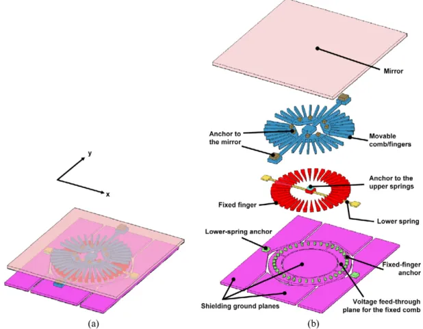
Figure 1. (a) Schematic diagram of the two-axis MEMS scanner with radial vertical combdrive actuators and a cross-bar spring structure.
(b) An imaginarily dismantled device.
by others; however, their achieved rotation angle was relatively small (2 mrad) [20]. Also, their architecture makes it relatively challenging to reduce the form factor. In our device, we adopt the cross-bar spring structure of our previous scanner [21,22], which consists of lower and upper torsion springs to obtain two rotational degrees of freedom (DOFs) without the use of gimbals. Both the actuators and the torsion springs are hidden under the mirror to reduce the device form factor for a given mirror area. This further helps to achieve a high fill factor when replicating such a scanner to form a 1D or 2D array. Also, a small form factor implies a small device footprint and package size, which is particularly important for applications such as MEMS-based endoscopic imaging. Previously, we have demonstrated the basic design concept and preliminary results [23]. In this paper, we include the detailed design, analysis, characterization, and discussion.
2. Device structure
Figure 1(a) is a schematic drawing of the two-axis scanner. It is imaginarily dismantled into four tiers in figure 1(b) for a clearer illustration. The device design is based on the SUMMiT-V surface micromachining process offered by Sandia National Laboratory. The layers used in the SUMMiT-V process are shown in figure 2. There are five polysilicon layers, including one nonreleasable ground/shield layer (mmpoly0) and four structural layers (mmpoly1 to mmpoly4). The polysilicon is deposited with low-pressure chemical
Figure 2. Layers in the SUMMiT-V process.
vapour deposition (LPCVD) and doped with phosphorous. Tetraethylorthosilicate silicon dioxide serves as the sacrificial layers. The mmpoly0 layer is used for the interconnecting lines, voltage feed-through lines/planes for the fixed combs, and shielding ground planes. The shielding ground planes minimize the area of exposed dielectric. This makes the mirror immune from drift caused by the dielectric charging effect. The lower torsion springs and the fixed combs are made of the mmpoly1 (1 µm thick) layer and the laminated mmpoly1+ mmpoly2 stack (2.5 µm thick), respectively. Both the upper torsion springs and movable combs are fabricated with the mmpoly3 layer (2.25 µm thick). This unique multilayer spring design enables us to achieve large clearance for both rotation axes: 6.5 µm (2 µm + 2.5 µm + 2 µm) and 6.25 µm (2 µm+2.25 µm+2 µm) for x- and y-axis rotations, respectively [21]. The top polysilicon layer, mmpoly4 2
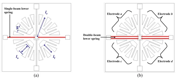
Figure 3. Layouts of the devices with (a) single-beam lower springs and (b) double-beam lower springs.
(2.25 µm thick), is used for the mirror. Before depositing the top two polysilicon layers mmpoly3 and mmpoly4, a CMP (chemical mechanical planarization) process is performed on their corresponding underlying SiO2sacrificial layers (denoted
by sacox3 and sacox4 respectively in SUMMiT-V) to eliminate the topography underneath the mirrors. It also provides a large gap spacing (10.75 µm) between the mirror and substrate. The mirror, movable combs, and torsion springs are mechanically and electrically connected through anchors. They are always grounded during operation as the lower springs are anchored to the shielding planes. The mirror is equipped with four quadrantally arranged sets of fixed combs, each anchored to its own voltage feed-through plane. Therefore, a maximum of four independent voltages can be applied to control the mirror. Our designs include several variants. Two types of cross-bar spring structure are deployed: one with single-beam lower springs as shown in figures1and3(a); the other with double-beam lower springs (figure3(b)). g, lo, lf, and lr in figure3
are the gap between movable and fixed fingers, length of overlap between movable and fixed fingers, movable finger length, and distance from the movable finger tip to the device centre, respectively. The four quadrantally arranged electrodes are denoted by a, b, c, and d. The beam width of both the lower and upper springs is drawn as 1µm in the design layout. The beam length of the lower spring is 37.5 µm while that of the upper spring is 36.5 µm. The mirror size is 96µm × 96 µm. The dimensions are chosen for the MEMS wavelength-selective switch, which normally requires a 1D array of micromirrors with a size of 100–200µm [16,21]. The mirror alone can be extended for other applications without changing the dimensions of the actuators and springs. The initial finger gap of a certain mirror design is either 1, 2, or 3µm, with the finger width fixed at 1 µm. The finger length and finger overlap also vary among devices. The parameters for each device are listed in table1.
3. Theoretical analysis
The device simulation is done with ANSYS, a commercial software for multi-field analysis. The Young’s modulus,
Table 1. Device parameters.
Devices with single-beam lower springs Device number g (µm) lo(µm) lf(µm) lr(µm) A1 1 12.79 15.5 30 B2 4.95 10 30 E1 2 10.85 13.5 30 B1 6.86 9.5 30 D1 3 12.06 15 30 E2 7.72 10 30
Devices with double-beam lower springs
D3 1 12.79 15.5 30 C3 4.95 10 30 E6 2 10.85 13.5 30 E5 6.86 9.5 30 E4 3 12.06 15 30 E3 7.72 10 30
Poisson’s ratio, and mass density of polysilicon are set as 85.4 GPa, 0.22, 2329 kg m−3, respectively. The Young’s modulus here for the polysilicon of the SUMMiT-V process is based on our previous study [19]. Two element types are used in the ANSYS model. The electrostatic element is Solid 122, capable of solving the 3D spatial distribution of the electrostatic potential and field. The structural element is Solid 95, which provides the information of nodal displacements, from which the rotation angles can be derived. For dc analysis, voltages are applied on the electrode sets (a, b) and (a, c) to obtain the dc characterization for x - and y-axis rotations, respectively. The notations of electrodes are shown in figure3. The x -axis rotation is predominantly the torsion motion of the lower springs. On the other hand, the y-axis rotation is a combination of the upper-spring torsion mode and lower-spring rocking mode. This is mainly due to the fact that the lower-spring thickness 1µm is significantly smaller than the thickness of the upper springs 2.25 µm, making the lower springs relatively compliant to bend upward or downward.
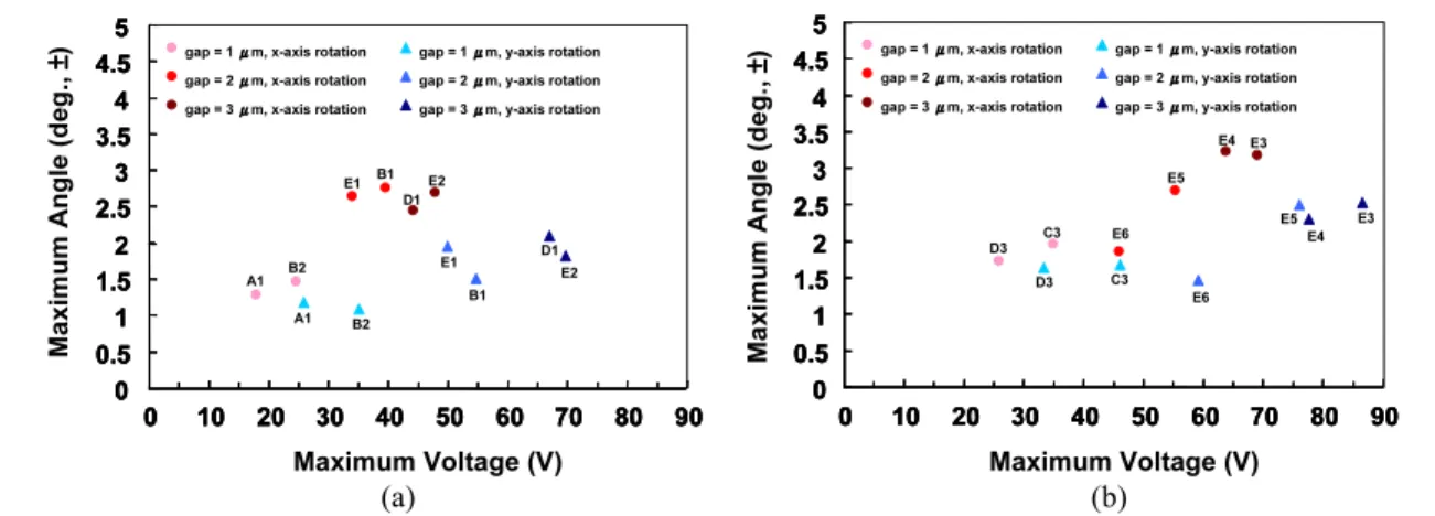
Figure 4 is the simulation results, showing the pull-in angle and the corresponding pull-in voltage for each device. The circular and triangular dots are for x - and y-axis rotations,
J. Opt. A: Pure Appl. Opt. 10 (2008) 044006 J-C Tsai et al
Figure 4. Simulation results for (a) devices with single-beam lower springs and (b) devices with double-beam lower springs.
respectively. Several trends can be observed in the charts. First, the pull-in angle of x -axis rotation is larger than that of y-axis rotation for each device. Also, for rotation about each axis, enlarging the initial finger gap tends to increase the pull-in angle and voltage. A device with double-beam lower springs tends to exhibit a larger pull-in angle and voltage at each axis than its counterpart with single-beam lower springs. These trends can be explained by the concept of lateral instability/pull-in. Combdrive actuators with smaller finger gaps are more susceptible to lateral instability. This issue stands out particularly for radial combdrive structures as the finger gap within a single device nonuniformly changes during rotation. Increasing the finger gap makes the device less susceptible to lateral pull-in, hence leading to a greater pull-in angle. The employment of the double-beam structure increases the ratios of ktwist/kx and ktwist/ky, where kx and ky are the
spring constants of the x - and y-axis rotations respectively, whereas ktwist is the spring constant for the in-plane twist
motion. A larger ktwist/kx or ktwist/ky ratio strengthens the
device resistance against lateral instability, therefore ideally yielding a larger pull-in angle.
We also observe that, with the same initial finger gap, decreasing the finger overlap length increases the pull-in voltages with slight changes in the angles. This is caused by the fact that a shorter overlap length results in a smaller capacitance, and therefore a higher voltage is required to reach a certain angle.
The results of modal analysis are shown in table2, which lists the mechanical resonant frequencies fx, fy, and ftwist of
the lowest-three-order modes, x -axis rotation, y-axis rotation, and in-plane twist, respectively. The frequencies within a certain column vary slightly from each other as their moments of inertia are not exactly identical due to different comb parameters. For a device with single-beam lower springs, the twist mode exhibits a slightly lower resonant frequency than the y-axis rotation mode. This is undesirable, as coupling between the rotation and the unwanted in-plane twist can easily occur under dynamic operation. Moreover, both ratios, ftwist/fx and ftwist/fy, of the double-beam devices are
respectively larger than their counterparts of the single-beam devices. This implies larger ktwist/kx and ktwist/ky, desirable
as mentioned above. Therefore, devices with double-beam
springs prevail in these regards. Furthermore, fx is smaller
than fyfor each device, i.e., kx < kyor ktwist/kx > ktwist/ky.
Based on the concept of lateral instability, this explains why
x -axis rotation exhibits a larger angle than y-axis rotation for
each device.
4. Device characterization and discussion
Figure 5 shows the scanning electron microscopy (SEM) photographs of the fabricated devices. The images are taken after a 45 min HF release process of oxide etching, CO2
supercritical drying, and metallization. The metallization process deposits 50 ˚A thick Cr and 2000 ˚A thick Au to enhance the reflectivity of the mirror surface. The mirror in figure5(a) is intentionally cut into a circular shape to reveal the underlying structures. This particular device has single-beam lower springs. The upper torsion springs are not shown in the photograph as they are hidden under the bars extruding from the circular mirror. Figure 5(b) is photograph of a standard device with a square mirror. The gutter-like structures work as on-chip shadow masks that prevent electrical shorting between electrodes after the metallization. The radius of curvature of the mirror is>100 mm before metallization and 45 mm after depositing the high-reflection Cr/Au coating. This curvature is acceptable for a MEMS wavelength-selective switch [16].
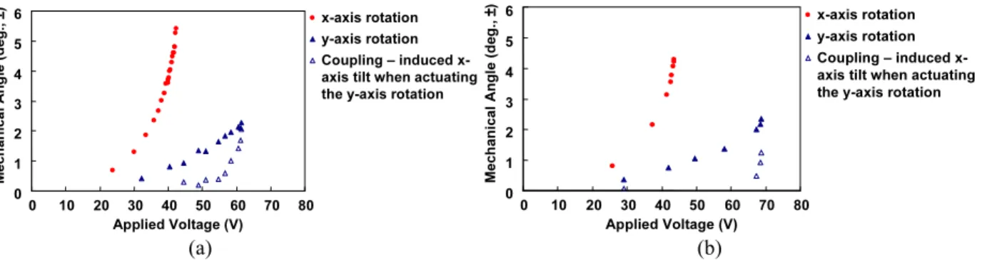
Figure6(a) is the measured dc characteristic of device E6 (double-beam lower springs, 2 µm initial finger gap). The mechanical scan angles are±5.4◦at 42 V and±2.3◦at 61 V for rotations about the x -axis and the y-axis, respectively. The measurement result of device E4 (double-beam lower springs, 3µm initial finger gap) is shown in figure6(b). The angles are
±4.3◦ (44 V) and±2.35◦ (69 V) for x - and y-axis rotations,
respectively. For both devices, rotation about the upper springs is more susceptible to lateral instability due to the asymmetric spring structure (ktwist/ky < ktwist/kx) and therefore has a
smaller scan range, as anticipated by the simulation. With a symmetric spring design, the scan angles for the two axes are expected to balance. As shown in the plots, an induced x -axis tilt caused by coupling is observed while actuating the y-axis rotation.
A discrepancy between the experiment and simulation is observed with regard to the absolute values of angles. Also, 4
Figure 5. SEM photographs of (a) a device with a circular mirror and (b) a standard device with a square mirror. (Reprinted from [23] with permission.© 2007 IEEE.)
Figure 6. Measured dc characteristics of (a) device E6 (double-beam lower springs, 2µm initial finger gap) and (b) device E4 (double-beam
lower springs, 3µm initial finger gap).
Table 2. Results of modal analysis. The resonant frequencies of the lowest-three-order modes are listed.
Devices with single-beam lower springs Device number Mode 1 Mode 2 Mode 3
A1 13 147 21 339 21 074 B2 13 119 21 289 20 994 E1 13 179 21 401 21 122 B1 13 138 21 335 21 063 D1 13 229 21 463 21 197 E2 13 205 21 424 21 133
Devices with double-beam lower springs D3 18 712 23 796 34 989 C3 18 645 23 705 34 890 E6 18 754 23 833 35 096 E5 18 706 23 811 35 012 E4 18 819 23 910 35 202 E3 18 711 23 864 35 134
J. Opt. A: Pure Appl. Opt. 10 (2008) 044006 J-C Tsai et al
Figure 7. Simulation results for different spring widths: (a) device E6 and (b) device E4. The numbers in parentheses of the legends are the
lower-spring beam widths. The measured data are plotted with red (x-axis rotation) and blue (y-axis rotation) dashed lines for comparison.
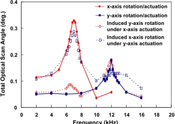
Figure 8. The frequency responses of device E6. The applied
sinusoidal signals have amplitude of 10 V.
the measured x - and y-axis angles of device E6 are larger than those of device E4, respectively, contrary to what the simulation has predicted. To address these issues, we first vary the spring beam width in the simulation and investigate the changes in the outcome. In a previous SUMMiT-V run [19] we verified an undercut of 0.13 µm on each side resulting from the etching of poly0 springs during that SUMMiT-V run. This effectively narrowed the spring width to 0.74 µm for an originally 1µm spring width design. Here, for the devices E6 and E4 we change the lower-spring beam width from 1 to 0.74, 0.66 and 0.59 µm in the ANSYS simulation for comparison. It can be seen in figure7that an undercut at the springs plays a significant role in the device characteristic, especially for x -axis rotation.
Moreover, other deviations during the device fabrication may occur; for example, the thickness of the CMP-processed sacrificial SiO2 layer, which is set as the nominal 2 µm in
the simulation, could eventually vary from run to run, falling within the range 1.9–2.4 µm for sacox3 and 1.7–2.2 µm for sacox4. These fabrication deviations along with the spring undercut may be the causes of the above discrepancies between the measured results and theoretical predictions.
The resonant frequencies for the x -axis and y-axis rotations of device E6 are 7 and 12 kHz, respectively (figure8).
They are lower than the theoretical values in table2 for two major reasons: undercut at the springs during the etching steps and the additional inertia contributed by the coated Cr/Au. Coupling between the two rotational modes is also observed and shown. The red/blue dotted line is the frequency response of the induced y-axis/x -axis rotation under x -axis/y-axis actuation. The minor peak around 7 kHz/12 kHz in the red/blue dotted line results from the x -axis/y-axis rotation, which is however detected by the position sensing detector due to slight system misalignment. More experimental measurements of the resonant frequencies as well as dc characterization of other devices are still in progress. The actual layer thicknesses and amount of spring undercut will also be determined to further improve the simulation model.
5. Conclusions
We have demonstrated novel two-axis MEMS scanners with radial vertical combdrive actuators. The mirrors are designed based on the SUMMiT-V surface micromachining process. Cross-bar spring structures are used to achieve dual-axis rotation. Both the radial vertical combdrive actuators and torsion springs are hidden underneath the mirror to achieve small form factors. Theoretical simulations under various device parameters are performed. Preliminary experimental results are also obtained. For one of the devices, the measured mechanical scan angles are±5.4◦at 42 V and±2.3◦at 61 V for rotations about the x -axis and y-axis, respectively.
Acknowledgments
This work was supported by National Science Council of Taiwan under grants NSC 95-2221-E-002-053 and NSC 96-2221-E-002-198-MY2, Excellent Research Projects of National Taiwan University, 95R0062-AE00-06, and DARPA/SPAWAR under contract N66001-00-C-8088.
References
[1] Fan L et al 2002 Digital MEMS switch for planar photonic crossconnects OFC 2002: Proc. Optical Fiber
Communication (Anaheim, CA) pp 93–4 Paper TuO4
[7] Freeman M O 2003 Miniature high-fidelity displays using a biaxial MEMS scanning mirror Proc. SPIE4985 56–62
[8] Chong C et al 2006 Optically modulated MEMS scanning endoscope IEEE Photon. Technol. Lett.18 133–5
[9] Aguirre A D, Hertz P R, Chen Y, Fujimoto J G,
Piyawattanametha W, Fan L and Wu M C 2007 Two-axis MEMS scanning catheter for ultrahigh resolution three-dimensional and en face imaging Opt. Express
15 2445–53
[10] Xie T, Xie H, Fedder G K and Pan Y 2003 Endoscopic optical coherence tomography with a modified
microelectromechanical systems mirror for detection of bladder cancers Appl. Opt.42 6422–6
[11] Toshiyoshi H, Piyawattanametha W, Chan C T and Wu M C 2001 Linearization of electrostatically actuated surface micromachined 2D optical scanner J. Microelectromech. Syst.10 205–14
[12] Yalcinkaya A D, Urey H, Brown D, Montague T and
Sprague R 2006 Two-axis electromagnetic microscanner for high resolution displays IEEE/ASME J. Microelectromech. Syst.15 786–94
[13] Piyawattanametha W, Patterson P R, Hah D, Toshiyoshi H and Wu M C 2005 Surface- and bulk-micromachined
two-dimensional scanner driven by angular vertical comb
wavelength-selective switch OSA Appl. Opt.46 3227–32
[18] Krishnamoorthy U, Lee D and Solgaard O 2003 Self-aligned vertical electrostatic combdrives for micromirror actuation IEEE/ASME J. Microelectromech. Syst.12 458–64
[19] Hah D, Huang S T Y, Tsai J C, Toshiyoshi H and Wu M C 2004 Low-voltage, large-scan angle MEMS analog micromirror arrays with hidden vertical comb-drive actuators IEEE/ASME J. Microelectromech. Syst.13 279–89
[20] Noell W et al 2006 Compact and stress-released piston tip-tilt mirror Proc. IEEE/LEOS Optical MEMS 2006 (Big Sky, Montana, August 2006) pp 40–1
[21] Tsai J C and Wu M C 2005 Gimbal-less MEMS two-axis optical scanner array with high fill-factor IEEE/ASME J. Microelectromech. Syst.14 1323–8
[22] Kim J H, Lee H K, Kim B I, Jeon J W, Yoon J B and Yoon E 2003 A high fill-factor micro-mirror stacked on a crossbar torsion spring for electrostatically-actuated two-axis operation in large-scale optical switch Proc. MEMS (Kyoto) pp 259–62
[23] Chiou S J, Hsieh T L, Tsai J C, Sun C W, Hah D and Wu M C 2007 A two-axis MEMS scanner driven by radial vertical combdrive actuators Proc. 2007 IEEE/LEOS Int. Conf. on Optical MEMS and Nanophotonics (August 2007) pp 83–4