Solid phase epitaxy for low pressure chemical vapor deposition Si ®lms
induced by ion implantation
Peng-Shiu Chen
a, T.E. Hsieh
a,*, Chih-Hsun Chu
baDepartment of Materials Science and Engineering, National Chiao Tung University, Hsinchu, Taiwan bUnited Silicon Inc., Hisnchu Science-based Industrial Park, Hsinchu, Taiwan
Received 9 February 1999; received in revised form 1 July 1999; accepted 1 July 1999
Abstract
This work investigated the ion implantation induced solid phase epitaxy (SPE) of Si thin ®lms prepared by low pressure chemical vapor deposition (LPCVD). Previous studies indicate that the residual layer at the interface between the Si thin ®lm and single crystalline substrate is the major obstacle to the SPE process of Si ®lm. In this work, Ge1and Si1ion were implanted to completely amorphize the Si ®lm
prepared by LPCVD. Ion implantation also mixed the interfacial oxide layer and its effects on subsequent epitaxial growth of Si ®lm subjected to various annealing conditions were discussed as well. In addition, the specimen surface was modi®ed by inductive couple plasma (ICP) process. The ICP modi®cation using nitrogen gas could form a vacancy source on the sample surface to enhance the atomic diffusion rate and change the stress state in the vicinity of surface, thereby accelerating the SPE process. q 1999 Elsevier Science S.A. All rights reserved.
Keywords: Chemical vapour deposition; Epitaxy; Ion implantation; Transmission electron microscopy
1. Introduction
Owing to its excellent uniformity and step coverage prop-erties, LPCVD is frequently applied to prepare Si thin ®lms in the ULSI processing. The as-deposited ®lm is amorphous, necessitating its transformation into a single crystalline state for further applications. However, according to previous investigations, the thin native oxide residing at the original amorphous/crystalline (a/c) interface impedes the epitaxial process. A clean interface is hence required to ensure good crystallinity of the regrown Si ®lms. Many processing tech-niques have been reported to remove the interfacial oxide [1±8]. Murakami et al., performed in situ Ar sputtering followed by annealing at 6808C to clean the surface of Si substrate in a chamber for ultra-high vacuum chemical vapor deposition (UHVCVD) [1]. Following deposition, the Si ®lm was further densi®ed by an annealing treatment. For cleaning purposes, Sasaki et al., reported an outgassing process at 8308C for 10 min prior to UHVCVD [2]. By dipping the Si substrate in an HF solution before loading it into CVD vacuum chamber, Hung et al., achieved epitaxy in the deposited ®lms [3]. Kuni et al., etched the Si surface
by H2 gas at 11008C, followed by HCl gas at deposition temperature before CVD process [4]. Without precleaning, transient annealing involving liquid phase [5] and ion implantation [6±8] have been performed to achieve epitaxy, respectively. Ion implantation has become a widely used method since, in addition to densifying and completely amorphizing the deposited Si ®lm, it can mix the native oxide layer at the original a/c interface. Csepregi et al., also found that ion implantation might suppress the random crystallization in Si ®lms [9].
The dependence of ®lm quality on the rate of regrowth has also received considerable attention in related studies. According to previous investigations. substrate crystallinity [9], annealing temperature [10], impurities in amorphous ®lm [11], and ion implantation dose and energy affect the rate of regrowth [12±13]. Csepregi et al., showed that the rate of SPE increased exponentially with the annealing temperature [9]. Their results indicated that residual oxygen, nitrogen and carbon atoms in amorphous Si ®lms decrease the SPE rate. When the impurity concentration exceeded the critical value of about 5 £ 1013 cm22, the SPE was nearly impossible and only polycrystalline phase was observed [13].
In this work, we deposit amorphous Si thin ®lms on Si substrate by LPCVD. The Ge1and Si1ions are implanted with various dose amounts and energies in order to
amor-0040-6090/99/$ - see front matter q 1999 Elsevier Science S.A. All rights reserved. PII: S0040-6090(99)00420-4
www.elsevier.nl/locate/tsf
* Corresponding author. Tel.: 13803; fax: 1 886-3-572-4727.
phize the sample as well as to induce ion mixing of the interfacial oxide. The redistribution of native oxide is moni-tored by secondary ion mass spectroscopy (SIMS) and the microstructure of the Si ®lms subjected to various annealing treatments is examined by transmission electron microscopy (TEM). This work also discusses the disruption of the oxide layer at various implantation conditions and its in¯uence on the rate of epitaxy and the morphology of the Si ®lms. The deposited ®lms are also modi®ed by ICP process to generate a defect source on the sample surface. Experimental results demonstrate that the rate of epitaxy is enhanced in Si ®lms using nitrogen as the reactive gas.
2. Experimental details
The (100), 3±5 V cm, n-type single crystalline Si wafer was ®rst cleaned by the standard RCA process. Before load-ing into the LPCVD chamber, the wafer was dipped in a 0.25% HF solution. The Si ®lm was then grown on at the pressure of 0.5 mTorr and substrate temperature of 5708C. The growth rate was about 0.03 nm/s and amorphous Si ®lms of 60±93 nm thick were prepared. Tables 1 and 2 list the conditions of ion implantation carried out in this study. Part of the specimens was subjected to dual implan-tation in which low-energy implanimplan-tation was performed to amorphize the deposited ®lm; meanwhile, high-energy implantation was performed to mix the oxides at the original a/c interface. The ICP modi®cation using either nitrogen (ICPN) or oxygen (ICPO) gas was performed in a micro-wave plasma chamber operating at the power of 250 W for 15 min. The specimen subjected to various treatments was then annealed in nitrogen ambient at temperatures ranging from 550 to 10008C for various time intervals so that the SPE might proceed. Following heat treatment, the speci-mens were thinned properly and transferred to a JEOL-200CX or Hitachi H-600 TEM to investigate their micro-structure. The specimens were also sent to a CAMECA IMS-4f SIMS for chemical composition analysis.
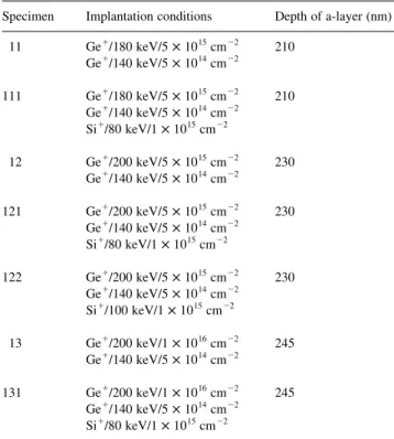
Full-cascade Monte Carlo simulations of Ge1ion implan-tation at 110, 135, and 200 keV were performed with TRIM 91.14 [14] using a value of 12 eV [15] for displacement energy and 2 eV for binding energy. At least 10000 ions
Table 1
Implantation conditions for specimens containing 60 nm thick LPCVD layer
Specimen Implantation conditions Depth of a-layer (nm) 21 Ge1/110 keV/5 £ 1015cm22 150 Ge1/70 keV/5 £ 1014cm22 211 Ge1/110 keV/5 £ 1015cm22 Ge1/70 keV/5 £ 1014cm22 150 Si1/80 keV/1 £ 1015cm22 22 Ge1/125 keV/5 £ 1015cm22 Ge1/70 keV/5 £ 1014cm22 159 221 Ge1/125 keV/5 £ 1015cm22 159 Ge1/70 keV/5 £ 1014cm22 Si1/80 keV/1 £ 1015cm22 23 Ge1/135 keV/5 £ 1015cm22 168 Ge1/70 keV/5 £ 1014cm22 231 Ge1/135 keV/5 £ 1015cm22 168 Ge1/70 keV/5 £ 1014cm22 Si1/80 keV/1 £ 1015cm22 24 Ge1/90 keV/3 £ 1015cm22 130 241 Ge1/90 keV/3 £ 1015cm22 135 Si1/80 keV/1 £ 1015cm22
Fig. 1. Cross-sectional of specimen containing 60 nm LPCVD ®lm without ion implantation annealed at annealed at 6008C for 2 h.
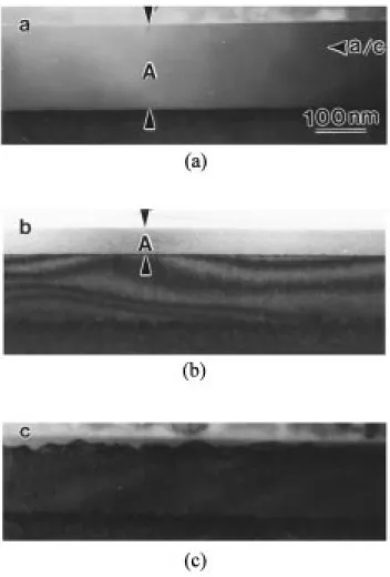
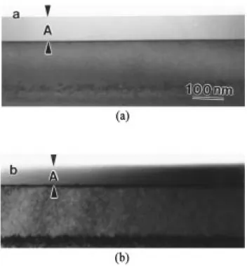
Fig. 2. Cross-sectional views of specimen 23: (a) as implanted (b) annealed at 5508C for 1 h and (c) annealed at 5508C for 4 h. (A: amorphous layer).
were accumulated to simulate the recoils of oxygen atoms for each implantation condition. For Ge1ions implanted at 110 and 135 keV, the thickness of SiO2layer was assumed to be 1.5 nm and the Si overlayer was 60 nm thick. For Ge1 ions implanted at 200 keV, the thickness of SiO2layer was assumed to be 2 nm and the Si overlayer was 93 nm thick. In the simulation, the density of SiO2was 2.27 g/cm3. 3. Results and discussion
3.1. As-deposited specimens
No epitaxy was observed in LPCVD Si ®lms without ion implantation regardless of the ®lm thickness and the condi-tions of subsequent annealing treatments. Polycrystalline Si grains were observed in the amorphous layer. Fig. 1 presents an example of such a mixed structure formed by a 6008C, 2-h annealing. According to TEM, polycrystallization always initiated at the interface containing native oxide, which totally suppressed the progress of epitaxial process. 3.2. Amorphous Si ®lms of 60 nm thick
3.2.1. A. Implanted specimen annealed at 5508C
Fig. 2a±c present the XTEM micrographs of specimen 23, subjected to dual Ge1 ion implantation at the conditions listed in Table 1 followed by annealing at 5508C for various time intervals. Fig. 2a indicates that the high-energy ion bombardment produces an amorphous layer of 168 nm thick. Fig. 2b shows the microstructure of the specimen annealed at 5508C for 1 h. At this temperature, the rate of SPE is estimated to be 8.7 nm/min so that the SPE should be completed in less than 20 min [16]. Nevertheless, only the amorphous Si beneath the original a/c interface completed the epitaxy, as indicated in Fig. 2b. At 5508C, at least a 4-h
annealing is required to complete the SPE in this specimen (Fig. 2c). According to a related investigation, the oxygen concentration at the interface between deposited ®lm and substrate must range from 5 £ 1013 to 3:6 £ 1015 cm22 to
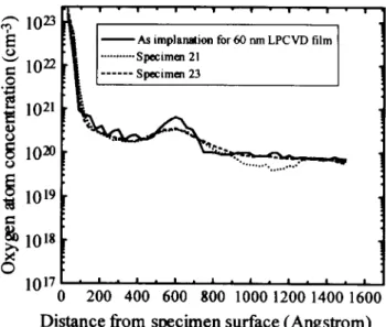
Fig. 3. SIMS analysis of oxygen concentration in specimen containing 60 nm LPCVD ®lm.
Fig. 4. (a) XTEM and (b) PTEM pictures of specimen 21 annealed at 6008C for 4 h; (c) XTEM and (d) PTEM pictures of specimen 23 annealed at 6008C for 4 h.
ensure the layer-by-layer SPE process [17]. The SIMS analysis in Fig. 3 indicates that although dual ion implanta-tion could smooth out the oxygen perturbaimplanta-tion, it could not reduce the oxygen concentration in the vicinity of original a/ c interface to such a level in specimens 21 and 23. Hence, retardation from the residual oxide occurred.
Kennedy et al., proposed that the SPE rate could be expressed in a form of 8.6 exp(20.9N) nm/min in which N denotes the oxygen concentration expressed in the units of 1020atoms/cm3[12]. Our SIMS analysis indicated that the maximum oxygen concentration in the vicinity of oxide interface was about 3:55 £ 1020 cm23for specimen 23. By substituting this value into the equation proposed by Kennedy et al., the lowest rate of SPE obtained herein is 0.3 nm/min at the original a/c interfacial regime. Since the
SPE rate was low, the {111} planes would bind the epitaxial wavefront when it swept across the oxide interface [18±20]. Fig. 2c con®rms this occurrence in which a hill-and-valley shape of epitaxial wavefront is observed.
3.2.2. B. Implanted specimen annealed at 6008C
In specimens 21, 22 and 23, the accelerating voltages of high-energy implantation were varied while the Ge1 dose amounts and the accelerating voltages of low-energy implantation remained the same. In these specimens, 1-h annealing at 6008C was insuf®cient to complete the SPE although their epitaxial wavefronts could sweep across the native oxide interface. In general, 2±3 h were necessary to complete the SPE, which depended on the ion implantation conditions. The specimen exhibited a higher rate of SPE when it was implanted at a higher energy level. For instance, according to our results, the epitaxial rate measured in specimen 23 was faster than that in specimen 21. This obser-vation indicates that high implantation energy can more effectively eliminate the epitaxial barriers supplied by the native oxide at original a/c interface.
Fig. 4 reveals many crystalline defects such as stacking faults and microtwins embedded in the regrowth ®lms. Comparison of the defect distributions in specimens 21 (Fig. 4(a),(b)) and 23 (Fig. 4(c),(d)) indicates that the speci-mens subjected to high implantation energy possessed epitaxial ®lms of a better quality. High implantation energy was more effective in smoothing out the oxide perturbation at the original a/c interface, subsequently reducing the number of oxide agglomerates in the vicinity of original a/c interface and ultimately the number of sites for defect nucleation during subsequent SPE process.
Computer simulation revealed that when accelerating voltage of Ge1 implantation was 110 keV, the energy absorbed by oxygen atoms at the depth of 60 and 62 nm beneath the specimen surface was 6.59 and 23.06 eV/AÊ per ion, respectively. The number of recoiled oxygen atoms was 19.8 per ion. When accelerating voltage of Ge1 implanta-tion was 135 keV, the energy absorbed by oxygen atoms at the depth of 60 and 62 nm beneath the specimen surface was 8.63 and 24.52 eV/AÊ per ion, respectively. The number of recoiled oxygen atoms was 20.8 per ion. Since the dose amount was 5 £ 1015 cm22, the total number of recoiled oxygen atoms was hence 9:9 £ 1016 and 1:04 £ 1017 cm22 for 110 and 135 keV implantation, respectively. This ®nding indicated that ion mixing became more effective when
Fig. 5. Cross-sectional view of specimen 221 annealed at 6008C for 1 h.
Fig. 6. Cross-sectional view of specimen 22 (a) annealed at 6008C for 4 h (b) modi®ed by ICPN and annealed at 6008C for 2 h and (c) specimen 221
increasing implantation energy. A relatively fast rate of SPE was therefore observed in specimen 23. Notably, such implantation energies were insuf®cient to cause a complete ion mixing, subsequently dampening the SPE in the vicinity of oxide interface although the epitaxial wavefront might sweep across the original a/c interface.
In addition to the dual Ge1ion implantation, part of the specimens (samples 211, 221, and 231) was further bombarded by Si1 with dose amount 1 £ 1015 cm22 and accelerating voltage 80 keV. In these specimens, the SPE could be completed in 1 h at 6008C, as revealed by TEM observations in Fig. 5. Apparently, such a Si1ion implanta-tion could remix the residual oxide in a more complete manner. It further reduced the barriers of SPE and improved the quality of epitaxial ®lm, as depicted in Fig. 5.
In this study, ICPN and ICPO modi®cations were also made on the specimen surfaces and the effect of plasma treatments on the epitaxial process was examined as well. Fig. 6 presents a series of XTEM micrographs for specimens 22 subjected to ICPN modi®cation followed by annealing at 6008C for various time intervals. According to this ®gure, the plasma surface modi®cation accelerated the rate of SPE. For instance, the SPE could be completed in less than 2 h in specimen 22. In addition to the faster epitaxial rate, a lower number of defects were observed, particularly in the speci-mens further subjected to Si1implantation (Fig. 6c). This occurrence might be attributed to that the nitride layer formed on the specimen surface could prevent the in-diffu-sion of oxygen during annealing, as the report of RaÈisaÈnen [21]. Furthermore, the nitride layer might serve as an effec-tive vacancy source, thereby promoted the SPE rate [22].
As to the specimens subjected to ICPO treatment, both ®lm quality and epitaxial rate were not improved (Fig. 7). For instance, specimen 22 could hardly complete the SPE in
Table 2
Implantation conditions for specimens containing 93 nm thick LPCVD layer
Specimen Implantation conditions Depth of a-layer (nm) 11 Ge1/180 keV/5 £ 1015cm22 210 Ge1/140 keV/5 £ 1014cm22 111 Ge1/180 keV/5 £ 1015cm22 210 Ge1/140 keV/5 £ 1014cm22 Si1/80 keV/1 £ 1015cm22 12 Ge1/200 keV/5 £ 1015cm22 230 Ge1/140 keV/5 £ 1014cm22 121 Ge1/200 keV/5 £ 1015cm22 230 Ge1/140 keV/5 £ 1014cm22 Si1/80 keV/1 £ 1015cm22 122 Ge1/200 keV/5 £ 1015cm22 230 Ge1/140 keV/5 £ 1014cm22 Si1/100 keV/1 £ 1015cm22 13 Ge1/200 keV/1 £ 1016cm22 245 Ge1/140 keV/5 £ 1014cm22 131 Ge1/200 keV/1 £ 1016cm22 245 Ge1/140 keV/5 £ 1014cm22 Si1/80 keV/1 £ 1015cm22
Fig. 8. Cross-sectional views of (a) specimen 24 (b) specimen 241 and (c) specimen 24 subjected to ICPN modi®cation. All specimens were annealed at 6008C for 4 h.
Fig. 9. (a) The BF cross-sectional view of specimen 21 and (b) the BF cross-sectional view of specimen 22. All specimens were annealed at 8008C for 30 min.
1 h. This dif®culty was attributed to that instead of pumping the vacancies in, the surface layer induced by ICPO process injected interstitials into the specimens. This not only dampens the SPE process, but also suppresses the defect reduction capability provided by plasma process.
Furthermore, the modi®cation of ICPN and ICPO on the surface might change the stress status in the vicinity of the surface of Si ®lms. According to Osada et al., the silicon nitride overlay ®lm on Si resulted tension stress on the ®lm [23], while the silicon oxide ®lm grown on Si produced compression stress [24]. Aziz et al., suggested that the tension stress enhance the SPE rate but not the compression stress [25]. We believed that the surface stress status also affects the SPE rate. Hence, the SPE rate was accelerated by ICPN treatment which produced tension stress on the sample surface.
Our results also suggest a low limit condition of Ge1ion implantation to achieve satisfactory results of SPE. For specimen 24 subjected to low energy (90 keV) and low dose amount (3 £ 1015 cm22) Ge1 implantation, only small protrusions of SPE wavefront were found at the origi-nal a/c interface after a 6008C, 4-h annealing (Fig. 8(a)). Such an ion implantation could not break the native oxide layer effectively, thereby inhibiting the epitaxial growth. Specimen 24 was further bombarded by Si 1 ion at 80
keV with dose amount 1 £ 1015 cm22(i.e. specimen 241) and its SPE behavior was again examined. Although the SPE was completed in 4 h at 6008C, the ®lm quality of specimen 241 was much inferior to that of specimens subjected to high implantation energy and dose amount, as illustrated in Fig. 8(b). Without substantial remix of oxide, subsequent ICPN modi®cation only slightly elevated ®lm quality in this specimen, as revealed by Fig. 8(c).
3.2.3. C. Implanted specimen annealed at higher temperatures
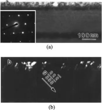
Fig. 9(a),(b) depict the bright ®eld XTEM micrographs of specimen 21 and 22 annealed at 8008C for 30 min, respec-tively. In comparison with the microstructure shown earlier, these specimens contain less crystalline defects in the epitaxial layer. The number of defects was further reduced with an increase of annealing temperature (e.g., specimen 23 annealed at 10008C for 10 min as shown in Fig. 10). At such a high temperature, the regrowth rate was fast and the residual oxide exhibited little dampening effects on the SPE process [26]. The epitaxy could proceed within a layer-by-layer manner and high quality ®lm was obtained. According to a previous investigation, direct annealing at high temperatures (.9008C) might produce polycrystalline structure in epitaxial layers [18]. However, our experimen-tal results indicated that at temperatures up to 10008C, high quality single crystalline layer could form in the specimen subjected to appropriate ion implantation (Fig. 10).
In addition, a two-step annealing process was carried out in specimens 22 and 23, and its effects on defect removal were examined as well. The annealing sequence was a 6008C annealing for 1 h followed by a 8008C annealing for 30 min or a 9008C annealing for 20 min. The BF pictures in Fig. 11 reveal that the epitaxial ®lms have a crystalline quality similar to those subjected to direct annealing at high temperatures. This observation demonstrates that annealing
Fig. 10. The BF cross-sectional view micrographs of specimen 23 annealed at 10008C for 10 min.
Fig. 11. (a) The BF cross-sectional view of specimen 22 annealed at 6008C for 1 h followed by 8008C for 30 min and (b) the BF cross-sectional view of
temperature also plays an important role in improving ®lm quality [26].
3.3. Amorphous Si ®lms of 93 nm thick
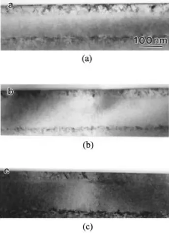
TEM observation revealed that dual Ge1 implantation with the conditions listed in Table 2 generated the amor-phous layers of thickness 210, 230 and 245 nm in specimens 11, 12 and 13, respectively. Fig. 12 summarizes the SIMS analyses for as-deposited specimen, specimens 12 and 13. According to this ®gure, the dual ion implantation can lower the concentrated oxygen at the native oxide layer. However, the TEM micrograph in Fig. 13 indicates that during the 4-h annealing at 6008C, the native oxide layer in specimens 11, 12 and 13 retained its integrity that the wavefront of SPE could not sweep across the native oxide interface. The amorphous CVD layers in these specimens were trans-formed into a mixture of polycrystalline and amorphous Si when the annealing duration was extended to 24 h, as shown in Fig. 14. Comparing the implantation conditions listed in Tables 1 and 2 reveals that that the Ge1 implanta-tion energies were higher in this part of the experiment. Unfortunately, such a high-energy Ge1implantation could not break up the oxide layer in the specimens containing 93 nm thick amorphous layer. During annealing, the SPE was always impeded a situation in which the nucleation and growth of polycrystalline Si grains became the dominant process for structural transformation. Hence, polycrystalline Si layers were found in specimens 11, 12 and 13.
In the case of 200 keV implantation, computer simulation revealed that the energy absorbed by oxygen atoms at the
depth of 93 and 96 nm beneath the specimen surface was 1.76 and 8.65 eV/AÊ per ion, respectively. The number of recoiled oxygen atoms would be 25 per ion and the total number of recoiled oxygen atoms was 2:6 £ 1017 cm22 when the dose amount was 1 £ 1016cm22. At this implanta-tion energy, the ion mixing remained incomplete to the extent that the SPE was inhibited in specimens listed in Table 2.
Next, the annealing temperature was increased to 8008C for specimen 13 to promote the SPE growth. The TEM investigation revealed that such a treatment produced a heavily twinned layer, as shown in Fig. 15. Although the epitaxial rate was raised with an increase of annealing temperature, too many nucleation sites were found for poly-crystalline grains due to an insuf®cient mix of native oxide. Epitaxy as well as the nucleation and growth of polycrystal-line grains proceeded at this temperature, resulting in a highly defective structure.
To further remix the native oxide layer, a part of the specimens was bombarded by Si1 ion at 80 keV with a dose amount of 1 £ 1015 cm22 (i.e. specimens 111, 121 and 131). Nevertheless, in specimens annealed at 6008C for 4 h, TEM investigation shown in Fig. 16(a) indicated that such an implantation remained insuf®cient to accelerate the SPE process. Specimen 12 was also bombarded by Si1 ion at 100 keV with the same amount of dose (i.e. specimen 122). However, only a small amount of extrusion was observed at the original a/c interface after annealing the specimen at 6008C for 4 h (Fig. 16(b)). Apparently, the conditions of ion implantation should be readjusted so that
Fig. 13. Cross-sectional views of (a) specimen 12 and (b) specimen 13 annealed at 6008C for 4 h. (A: amorphous layer)
Fig. 14. Cross-sectional views of (a) specimen 12 and (b) specimen 13 annealed at 600 8C for 24 h. (A: amorphous layer)
a substantial oxide remix at the original a/c interface could be obtained to promote the SPE process.
4. Conclusions
This work elucidates the SPE behaviors of LPCVD Si layer using ion mixing technique. Experimental results indi-cate that SPE process and nucleation and growth of poly-crystalline structure are two competing processes during the annealing of amorphous LPCVD ®lms. When ion implanta-tion can break up the native oxide, the epitaxial wavefront can sweep across the original a/c interface to complete the SPE growth. High energy implantation and an increase of annealing temperature not only raise the swiftness of SPE process, the layer-by-layer growth is also promoted and an epitaxial layer containing a relatively small amount of defects can be obtained as well. Our results further indicate that nucleation and growth of polycrystalline grains become a dominant mechanism of structure transformation when remix of oxide layer is insuf®cient. In these cases, the regrowth layer is polycrystalline or a mixture of polycrystal-line and epitaxial structures, depending on the conditions of subsequent annealing. Remixing of interfacial oxide becomes relatively dif®cult in the specimens containing thicker LPCVD Si ®lms. Although increasing the annealing temperatures can compensate for such a de®ciency, the epitaxial layers generally contain a large amount of crystal-line defects.
This work also investigates how plasma surface modi®-cation affects the SPE process of LPCVD Si layer. Accord-ing to those results, the SPE rate increases and the number of defects decreases when the specimens are subjected to the ICPN treatment. This is attributed to that the formation of nitride on specimen surface might serve as the oxygen diffu-sion barrier and vacancy source to promote the SPE rate. The tension stress induced by ICPN is also bene®cial to the SPE rate. In contrast, no enhancement is observed in the specimens subjected to ICPO treatment. The oxide layer might inject interstitials into the specimens to annihilate the vacancies inside, thereby reducing the mobility of atoms and ultimately dampening the SPE process.
Acknowledgements
The authors would like to thank the National Science Council of the Republic of China for ®nancially supporting this research under Contract No. NSC88-2216-E009-013. References
[1] E. Murakami, M. Moniwa, K. Kusukawa, M. Miyao, T. Warabisako, Y. Wada, J. Appl. Phys. 63 (1998) 4975.
[2] M. Sasaki, T. Katoh, H. Onoda, N. Hirashita, Appl. Phys. Lett. 49 (1986) 397.
[3] L.S. Hung, S.S. Lau, M. von Allmen, J.W. Mayer, B.M. Ullrich, J.E. Baker, P. Williams, W.F. Tseng, Appl. Phys. Lett. 37 (1981) 909. [4] Y. Kuni, M. Tabe, K. Kajiyama, J. Appl. Phys. 56 (1984) 279. [5] S.S. Lau, W.F. Tseng, M.-A. Nicolet, J.W. Mayer, R.C. Eckardt, R.J.
Wagner, Appl. Phys. Lett. 33 (1978) 130. Fig. 15. (a) The BF picture with corresponding diffraction pattern and (b)
DF cross-sectional view of specimen 13 annealed at 8008C for 30 min.
Fig. 16. Cross-sectional views of (a) specimen 111 and (b) specimen 122 annealed at 6008C for 4 h. (A: amorphous layer).
[6] H. Yamamoto, H. Ishiwara, S. Furukawa, Jpn. J. Appl. Phys. 24 (1985) 411.
[7] R.C. Cole, J.F. Kundsen, R.C. Bowman Jr, P.M. Adams, J.P. Hurrell, L. Halle, R. Newman, D. Jamieson, J. Electrochem. Soc. 135 (1988) 974.
[8] I. Mizushima, H. Kuwano, T. Hamasaki, T. Yoshii, M. Kashiwagi, J. Appl. Phys. 63 (1988) 1065.
[9] L. Csepregi, J.W. Mayer, T.W. Sigmon, Appl. Phys. Lett. 29 (1976) 92. [10] A.J. Walker, P.H. Woeriee, H.G. Pomp, N.E.B. Cowern, J. Appl.
Phys. 73 (1993) 4048.
[11] C.P. Wu, J.T. McGinn, L.R. Hewitt, J. Electro. Mater. 18 (1989) 721. [12] E.F. Kennedy, L. Csepregi, J.W. Mayer, T.W. Sigmon, J. Appl. Phys.
48 (1977) 4241.
[13] M. von Allmen, S.S. Lau, J.W. Mayer, W.F. Tseng, Appl. Phys. Lett. 35 (1979) 280.
[14] J.P. Biersack, L.G. Haggmark, Nucl. Instrum. Methods 174 (1980) 257.
[15] J. Narayan, D. Fathy, O.S. Oen, O.W. Holland, J. Vac. Sci. Technol. A 2 (1984) 1303.
[16] S.S. Lau, W.F. van der Weg, in: J.M. Poate, K.N. Tu, J.W. Mayer (Eds.), Thin Films-Interdiffusion and Reaction, Chapter 12, Wiley, New York, 1978.
[17] A.V. Zotov, V.V. Korobtsov, J. Cryst. Growth 98 (1989) 519. [18] S.S. Lau, J. Vac. Sci., Technol. 15 (1978) 1656.
[19] R. Drosd, J. Washburn, J. Appl. Phys. 51 (1980) 4106. [20] R. Drosd, J. Washburn, J. Appl. Phys. 53 (1982) 397. [21] J. RaÈisaÈnen, Appl. Phys. A 30 (1983) 87.
[22] M. Fahey, P.B. Grif®n, J.D. Plummer, Rev. Mod. Phys. 61 (1989) 289. [23] K. Osada, Y. Zaitsu, S. Matsumoto, M. Yoshida, E. Arai, T. Abe, J.
Electrochem. Soc. 142 (1995) 202. [24] S.M. Hu, J. Appl. Phys. 70 (1995) R53.
[25] M.J. Aziz, P.C. Sabin, G.Q. Lu, Phys. Rev. B 44 (1991) 9812. [26] G.L. Olson, J.A. Roth, Mater. Sci. Rep. 3 (1988) 1.