almost no effect on the value of q : the difference between the q-values for a patch (broken curve) and a dipole (dotted curve) is less than 0.02 for E, = 2.55, and nearly zero for E, = 12.8.
As
we are only interested in resonant antennas, the length L of the patch is not of importance: it is determined by W , h, E, and the resonant frequency. Therefore only two parameters are needed to describe the space wave efficiency: E , and hi;.,. A first estimate of q uses a linear h / i , dependence:
The factor v 3 ( ~ r - I ) in the second term assures that q = 1 for an air dielectric, and that q decreases faster with increasing h / i , as c, increases. Eqn. 2 can also be written in terms of the cutoff frequency of the first-order T E mode:
with
.fil
= co/[4hJ(s, - l)] 1 00!\ (31 n O 5 0 i4
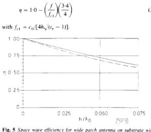
I 0 25- j 0 0 025 0 050 0 075 0 -h i -h o y s l Fig. 5 Space waue efflciencb for wide patch antenna on suhstrate with E , = 4 0patch’ ~ eqn 4
- - - -
From Figs 2 and 3, we see thdt the linear dependence works well for small h/no (until 0 06), but that for larger sub- strate thicknesses and small E, some extra terms are needed (For C, = 12 8 the linear curve is extended practically to the
point where the T E , mode can propagate) The final expres- sion for q is
(4) with H = d ’ ( ~ , - l)(h/E.,) = 0.25(ffc1).
In Figs. 2-6, the solid curve represents the results obtained with eqn. 4. As one can see, there is excellent agreement with the data from the Green function methods.
R a n g e of v a l i d i t y : For practical purposes, it is largely sufficient if q can be calculated for f < 0.8fcl, which is equivalent to
H < 0.20. For E, = 2.55 this corresponds to h / i o = 0.16, and
for E, = 12.8 to h / i , = 0.058. For this range of H a maximal
1 00 I
I
0 2 5 1 I I 01 0 001 002 003 0 0 4 005 h i h oL T
Fig. 6 Space wate efficiencj for wide and narrow patch antenna on whstrate with E, = 9 8
patch’ dipole’ ~ eqn 4
ELECTRONICS LETTERS 25th May 1989 Vol 25 N o 1 7
difference of 0.04 is found between eqn. 4 and Pozar’s results’ for a patch 0.3 io wide (Figs. 2 and 3). A similarly small devi- ation of 0.05 is found between eqn. 4 and Perlmutter’s’ results (Figs. 4, 5 and 6). As the difference between q for dipoles and patches is always less than 0.02, eqn. 4 also holds for dipoles. Conclusion: A very simple expression is presented that sum- marises the available data for space wave efficiency of rec- tangular microstrip antennas. Its arguments are E , and h/j.o. The expression is valid for dipoles and patches, and has been checked against numerical data for E, = 2.2, 2.55, 4, 9.8 and 12.8. The maximal difference between numerical data and the closed-form expression is 0.05 for
J ( E ,
- l)(h/i,) < 0.20.B NAUWELAERS 29th March 1989
A VAN DE CAPELLE Katholieke l~ niuervteit Leuven
Kardinaul Vert ierluun 94, B-3030 Leuven, Belgium D I L t S 4 T - T E L E M I C
References
POZAR, U . M. : ‘Considerations for millimeter wave printed antennas’, IEEE Trans., 1983, AP-31, pp. 74C747
R O U I ~ T , B., MOSIG, J . R., and GARDIOL, F. E.: ‘Puissance et rende- ment associes aux antennes microruban’. Proc. JINA ’89, Nice, France, 1989, pp. 232-236
BHATTACHARYYA, A. K., and GARG, R. G . : ‘Effect of substrate on the efficiency of an arbitrarily shaped microstrip patch antenna’. IEEE Truns., 1986. AP-34, pp. 1181-1188
PERLWTTER, P., SHTRIKMAN, s., and TREVES, D.: ‘Electric surface current model for the analysis of a microstrip rectangular element’. 1984 IEEE int. symp. digest on antennas and propagation, Boston, 1984, pp. 577-580
PERLMUTTER, P., SHTRIKMAN, s., and TREVES, D . : ‘Electric surface current model for the analysis of microstrip antennas with applica- tion to rectangular elements’, IEEE Trans., 1985, AP-33, pp. 301-311
ROUDOT, B., TERRET, c., DANIEL, J . P., PRIBETICH, P., and KENNIS, P.: ‘Fundamental surface-wave effects on microstrip antenna radi- ation’, Electron. Lett., 1985, 21, pp. 11 12-1114
MOINI, R., HERAULT, J . , and JECKO, B.: ‘Influence des ondes de surface sur la puissance rayonnee par des antennes microruban’. Proc. JINA ‘89, Nice, France, 1989, pp. 26G-263
PERFORMANCE ANALYSIS OF
R A M A N A M P LI FICATIO N
HIGH-DENSITY W D M SYSTEMS USING
Indexing terms: Optical communications, Optical fibres, Non- linear optics, Multiplexing
The applications of Raman amplifiers as repeater amplifiers or post-transmitter amplifiers in a high-density WDM system are theoretically investigated. There exists an optimum pump power which results in maximum amplifier gain. The result shows that amplifier gains up to 50dB and 20dB are achiev- able for use as a repeater and a post-transmitter amplifier, respectively.
Introduction: High-density, wavelength-division-multiplexed ( H D W D M ) systems provide a means for exploiting the vast bandwidth of a single-mode fibre.’ One of the limitations imposed on an H D W D M system is the power depletion caused by stimulated Raman scattering (SRS),2.3 so that both the number of channels and transmission power are limited. On the other hand, SRS can be used to optically amplify multichannel signals with single pump power,4 which is of special interest in an H D W D M system. The fibre Raman amplifier can be either used as a repeater amplifier to boost weak signals, or used at the transmitting end to amplify the multichannel signals so as to increase system transmission distance and relax the limitation caused by SRS. This letter investigates the application of Raman amplification in an H D W D M system.
Analysis: The nonlinear pumping process in an H D W D M system is complicated and depends on channel spacing, number of channels, as well as the pump and signal powers. Here we analyse the signals of an N-channel H D W D M fibre transmission system with Raman amplification, and consider the case that all signals are pulse-modulated while the pump is a continuous wave.
Let A and a denote the effective cross-section and loss coef- ficient of the fibre, respectively. To simplify the analysis, we assume that the Raman gain has a Lorentzian lineshape, while the actual lineshape in fibres is much more ~ o m p l i c a t e d . ~ The lineshape is given as
so(w/2)2
g ( V R ) = ( V R - V O ) Z
+
(w/2)2where yo is the peak Raman gain coeficient, w the full width at half-maximum of the Lorentzian lineshape, v R the Raman shift between the two coupling waves, and vo the Raman shift corresponding to the peak gain.
Let v P and vSi denote the lightwave frequencies of the pump and the ith signal in the H D W D M system. In an H D W D M system the linewidths of the signals are much smaller than w, and hence the Raman gain for the signals is assumed to be constant. The Raman gain constant coupling the pump and the ith signal,
si,
and the gain constant coupling the ith and jth signal channels, gij, can then be calculated from eqn. 1with appropriate v R .
Let L denote the transmission distance. The signal power Si(0), i = 1, 2, . . . , N, and the pump power P ( 0 ) are injected at z = 0 and travel in the + z direction. The differential equa- tions governing the signals and the pump propagation are given by
d z A
(3)
Here we assume vSl > vS2 ... > vSN and that the N channels
are equally spaced with channel spacing AV. The second term in eqn. 2 denotes the coupling between the ith signal and the pump; the third and the last terms express the crosscoupling among the signal channels. Because of the crosscoupling among the signal channels, the optical power of the shorter- wavelength channels will be depleted by the longer- wavelength channels, and will be most severe for the shortest-wavelength channel (channel 1). As a result, the system transmission distance will be limited by the achievable amplifier gain of channel 1. Numerical calculation is carried out to estimate the achievable amplifier gain. We consider the worst case that all the channels are in the 'on' state, in which channel 1 is most depleted. For simplicity we choose an odd number of channels, and locate the middle channel at the centre of the Raman gain profile. The amplifier gain of channel 1 at z = L is defined as
(4) where S , ( L ) is the power of channel 1 at z = L with Raman
amplification.
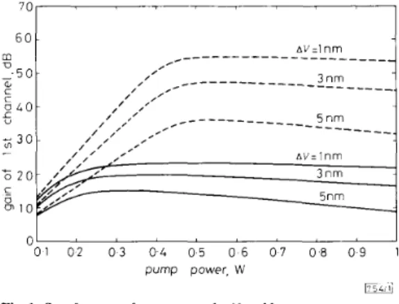
The relationship between the gain of channel 1 and the pump power is shown in Fig. 1. Here two regions can be characterised. One is the linear region in which G increases linearly with P(O), while the other is the saturation region where G gradually reaches a maximum value and decreases as
P(0) further increases. For use as post-transmitter amplifiers
(SXO) = 0.1 mW), the achievable gain is much smaller and the maximum gain occurs at a lower pump power level than those used as repeater amplifiers (SAO) = 0.1 pW). The influence of channel number N on G is shown in Fig. 2, where g1 and the
698
total signal span ( N - 1) AV are kept constant. The degrada- tion of G as N increases is expected since more power of channel 1 is depleted. When used as repeater amplifiers, G is insensitive to the channel number N in the linear region but degrades in the saturation region. In the linear region, because channel 1 obtains much more power from the pump than that depleted by the other channels, G is nearly independent of N .
-7
0 1 02 0 3 0 4 0 5 0 6 07 0 8 0 9 1 pump power, W
Fig. 1 G as function of pump power for N = I I
Solid lines (post-transmitter amplifiers): SAO) = 0.1 mW; broken lines (repeaters): SAO) = 0.1 pW. For convenience we use wave- length unit for AV. go = 7.5 x lO-I4m/W, A = 5 x 10-L1m2, a = O.ZdB/km, W = 240cm-', vo = 460cm-',L = 150km However, in the saturation region the depletion by the other channels becomes comparable to that obtained from the pump, and thus degradation results. Since it is essentially operating in the saturation region when used as a post- transmitter amplifier, G degrades as N increases. When the pump power increases, the signal power of channel 1 depleted by the other channels may exceed that obtained from the pump, so that the gain decreases. Therefore there exists an optimum pump power which results in maximum gain of channel 1. As shown in the Figures, for use as a repeater amplifier, an amplifier gain up to 50dB is achievable, which corresponds to 250 km repeater spacing for 0.2 dB/km fibre loss. For use as a post-transmitter amplifier, more than 20dB gain is still obtainable, corresponding to 100 km extended transmission length, and the constraint imposed by Raman crosstalk is relaxed because the depleted power of channel 1 by the other channels is compensated by the pump.
01
01 0 2 0 3 0 4 0 5 0 6 07 0 8 0 9 I pump p 0 w e r . W
1754/21 Fig. 2 Effect ofchannel number on G
Solid lines (post-transmitter amplifiers): SJO) = 0.1 mW; broken lines (repeaters): SXO) = 0.1 pW. Same parameters used as in Fig. 1; ( N - 1) Av = 40nm
Conclusions: We have investigated the properties of Raman amplification in an H D W D M system. The results show that there exists an optimum pump power to yield a maximum amplifier gain. A high gain is achievable for use as a repeater amplifier, and a modest gain is obtainable when used as a post-transmitter amplifier. Based on these results, we conclude
that Raman amplifiers are potential candidates to amplify multichannel signals in an H D W D M system.
M.4. K A O 29th March 1989
J. WU
Department of Electrical Engineering National Taiwan University
Taipei, Taiwan 10764, Republic of China References
KOBRINSKI, H., et al.: ‘Demonstration of high capacity in the LAMBDANET architecture: a multiwavelength optical network’, Electron. Lett., 1987, 23, pp. 824-826
CHRAPLYVY, A. R., and HENRY, P. s.: ‘Performance degradation due to stimulated Raman scattering in wavelength-division-multi- plexed optical fibre systems’, ibid., 1983, 19, pp. 641-643
CHRAPLYVY, A. R . : ‘Limitations on lightwave communications imposed by optical fiber nonlinearities’. Tech. dig. opt. fiber commun. conf., 1988, p. 19
EDAGAWA, N., et al. : ‘Simultaneous amplification of wavelength- division-multiplexed signals by a highly efficient fibre Raman amplifier pumped by high-power semiconductor lasers’, Electron. Lett., 1987, 23, pp. 19&197
STOLEN, R . H., and IPPEN, E. P.: ‘Raman gain in glass optical wave- guides’, Appl. Phys. Lett., 1973, 22, pp. 276-278
FEMTOJOULE BISTABLE OPTICAL SWITCHING OF INHOMOGENEOUSLY PUMPED LASER DIODE AT 5 0 0 M H z USING MODE-LOCKED TUNABLE DIODE LASER
Indexing terms: Semiconductor lasers, Optical switching, Non- linear optics
We have investigated the nonlinear transfer characteristics and temporal response of bistable three-section lasers within a broad wavelength interval (30nm), when switched with picosecond optical pulses (20ps) at a high repetition rate. The minimum input coupled switch-on energy was 0.7 fJ. The shortest switching time was 60 ps.
In this letter we present results comparable to the lowest switching energies,’ and at the same time the highest repeti- tion rates’ reported for bistable optical devices.
E x p e r i m e n t : The bistable laser diode (BLD) was a three- section GaInAsP diode, with a lasing wavelength of 1310nm. The absorber section was situated at the facet where the optical switching pulses were incident. The bias currents were chosen so that the BLD was kept 0.1mA below the electrical switch-on threshold. Further details can be found in Reference 3.
We measured the photocurrent generated in the BLD when it was reverse biased to optimise and evaluate the input coup- ling efficiency, which was approximately 10%. A pinhole transmission measurement of the input spot size was in very good agreement with this input coupling efficiency.
A mode-locked diode laser was employed for switching the BLD. The mode-locked laser produced optical pulses of 2 C 40 ps F W H M , as measured by autocorrelation. These pulses were monitored on a sampling oscilloscope by using a p i n photodiode with a rise time of 60ps. The wavelength of the mode-locked laser was controlled by a Fabry-Perot etalon placed in an external cavity. The spectral width of the pulses was < 3 A for wavelengths less than 1300nm and < 5 A for longer wavelengths.
T o achieve fast switch-off 1 ns after the set-pulse, a short negative electrical pulse was employed to extract the charge carriers from the absorber section.’ The pulse amplitude was around 20mA and the pulse width was less than 130ps (FW HM).
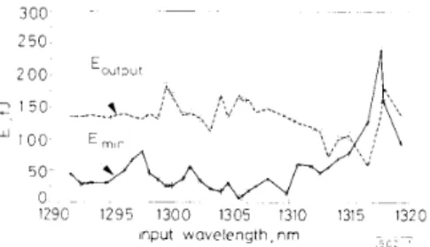
M i n i m u m switching e n e r g y : We measured the minimum input energy for switching E,,, in front of the microscope objective ELECTRONICS LETTERS 25th May 1989 Vol. 25 No. 7 1
for input coupling (NA = 0.83). The output energy E o u f p u f , when switching with minimum input energy, was measured after the microscope objective for output coupling (NA = 0.25). The results are plotted against input wavelength in Fig. 1, We found the smallest Emin to be 7.2 fJ, i.e. the input
coupled energy was approximately 0.7 fJ, at a n input wave- length of 1305.8 nm. This corresponds to less than 5000 input coupled photons. Another feature of the switching character- istics at 1305.8nm is the high output energy 170fJ. This optimum wavelength was 4 n m shorter than the main lasing mode of the BLD. We recorded the input and output spectra using a monochromator with a resolution better than 1
A.
There were three cmnmon features of all the output spectra obtained: ( a ) the attenuated transmitted input signal, ( b ) an initial lasing BLD-mode positioned quite near the input wave- length of (a), and ( c ) a broad dominating laser spectrum of the BLD which was centred at 1310nm. This implies that the BLD reaches the steady-state within 1 ns.
300
U - ~
129C 1295 1300 1305 1310 1315 1320
A
irput wavelength nm
Fig. 1 Minimum mitching energy E,,, plotted against input Havelength Output energy E,,,,,, corresponds to input energy E,,,
We investigated resonance effects by increasing the number of sampled input wavelengths within the interval for optimum switching energy. This was accomplished by temperature- tuning the mode-locked laser. The BLD was switched at several input wavelengths in the interval 1304.8-1306.1 nm and with a spectral width of the mode-locked laser pulse of
around 1.5
A
(FWHM). This was plotted with Emin and EoUfPUfagainst input wavelength, as in Fig. 1. The investigated inter- val was larger than the spacing of two internal cavity modes of the BLD. The wavelength difference of the reflected input pulse and the output pulse was simultaneously measured via a beam splitter placed between the mode-locked laser and the BLD. We found no clear resonant behaviour in this interval. T r a n s f e r ,function: In Fig. 2, we have plotted .EoUfPUf against
ELnpur for three different input wavelength intervals. The five points in the Figures are the mean values, within each of the three intervals, obtained for Einpuf equal to 0, E,,/2, Emin,
2E,,, and 4Emi,, respectively. T o obtain a measure of the spread of results within different input wavelength intervals, we calculated the standard deviations, which were plotted as error bars for EoUfPUf and Emin and Emin at each point. The nonlinear shape of the transfer characteristics is more pro- nounced for the optimum wavelength interval than for long wavelengths, as in Figs. 2b and c. The threshold behaviour observed in all three intervals confirms that we have true bistable switching at 500MHz. Although the set-up was not optimised for output coupling, the maximum pulse energy gain was 14dB.
Bistable switching t i m e : The shortest deconvolved rise time of the BLD signal was approximately 60ps when switching in the optimum wavelength interval with a high input energy. The BLD signal rises immediately after the input signal. The input coupled energy could be decreased to 29fJ without increasing the switching time. The maximum delay time was 0.7 ns, limited by the electrical reset 1 ns after the input pulse. S u m m u r y : We have characterised bistable switching of a three- section bistable laser diode in an input wavelength interval of
30nm and at d repetition rate of 500MHz. Bistable switching was performed with less than 5000 input coupled photons. The shortest recorded bistable switching time was approx- imately 60 ps.