結晶技術對複晶矽薄膜電晶體元件 特性及缺陷分布之影響
78
0
0
全文
(2) 結晶技術對複晶矽薄膜電晶體元件 特性及缺陷分布之影響 Device performance and defect analysis of poly-Si TFTs with various crystallization technologies 研 究 生: 王志宏 指導教授: 冉曉雯. Student: Zhi-Hong Wang Advisor: Dr. Hsiao-Wen Zan. 國立交通大學 電機學院光電顯示科技產業研發碩士班 碩士論文. A Thesis Submitted to College of Degree Program of Electrical Engineering and Computer Science National Chiao Tung University in Partial Fulfillment of the Requirements for the Degree of Master In Display Institute February 2007 HsinChu, Taiwan, Republic of China.. 中華民國九十六年二月.
(3) 結晶技術對複晶矽薄膜電晶體元件 特性及缺陷分布之影響 研究生: 王志宏. 指導教授: 冉曉雯 博士. 國立交通大學 電機學院. 摘要 為了提升複晶矽薄膜電晶體的特性,高品質的複晶矽薄膜是關鍵,而如何開 發低成本低溫的結晶技術,是整個低溫複晶矽面板技術再突破的首要之務;在本 論文內,我們比較四種結晶技術的薄膜品質,包含量產線之準分子雷射退火、固 態晶體雷射退火、固相退火及飛秒雷射退火四種結晶技術,並分析四種技術製作 之複晶矽薄膜電晶體的元件特性。其中,前三種結晶技術都是靠熱能結晶的技術, 而飛秒雷射退火則是新型非熱結晶技術,具有低雷射能量即可結晶之特性,是我 們此篇論文討論的重點技術。 飛秒雷射退火是利用長波長(800 奈米) 、低能量密度(約 45 mJ/cm2)之飛 秒雷射掃瞄非晶矽薄膜樣品以進行結晶,調整不同能量密度,可以變化樣品的結 晶性以及平坦度,本篇論文中利用 SEM、AFM、以及拉曼分析等技術,來分析此飛 秒雷射退火之最佳製程條件。同時,也製作了利用飛秒雷射退火結晶之複晶矽薄 膜電晶體,分析其元件特性和薄膜品質的相依性,在最佳結晶條件下,飛秒雷射 退火再結晶元件擁有如低的臨界電壓約 2.0 V、次臨界斜率趨近於 0.8 V / dec.、開 關電流比約 2.33 x 10⁷ 以及場效載子傳輸率約 62 cm2 / Vs,首次展示了非熱再結晶. i.
(4) 技術在製作複晶矽薄膜電晶體上的可行性,同時,和同樣製程下製作的固相退火 元件相比較,飛秒雷射退火之元件可以有較佳的特性。 最後我們針對不同的結晶技術去分析薄膜的缺陷分布情形,從次臨界斜率去 萃取斷鍵態(deep state)密度,並利用 I-V 變溫量測的活化能數據去萃取缺陷的能 態分佈,觀察扭曲鍵態(tail state)密度和場效載子傳輸率的關連性;最後,我 們從 C-V 量測觀察並討論缺陷態的頻率響應,並和元件的電流電壓特性做比對及 分析。. ii.
(5) Device performance and defect analysis of poly-Si TFTs with various crystallization technologies. Student: Zhi-Hong Wang. Advisor: Dr. Hsiao-Wen Zan. Degree Program of Electrical Engineering National ChiaoTung University. Abstract In order to improve the characteristics of poly-Silicon thin-film transistors (TFTs), the high quality of poly-silicon film is the key issue. And how to develop a low cost and low temperature crystallization technology is the prime mission of the whole LTPS panel technology. In this thesis, we compared the film qualities under four different crystallization technologies, including the mass production excimer laser annealing (ELA), solid state laser (SSL) annealing, solid-phase crystallization (SPC) and femtosecond laser annealing (FLA). Besides, we also analyzed the device performance fabricated by the four kinds of crystallization technologies. Since the former three crystallization technologies are crystallized by thermal energy, and FLA is a new, non-thermal crystallization technology which has the characteristics of crystallization formed by a lower laser energy density. Therefore, it is the main technology we discuss. iii.
(6) in the thesis. Amorphous-silicon film crystallized by line-scan near-infrared femtosecond laser annealing, which is long wavelength (800 nm), low energy density (about 45 mJ/cm2). As we adjusted different laser energy density, we could change the crystallinity and the roughness of the sample. In this thesis, we introduced the SEM, AFM, and Raman analysis to find out the best process condition of FLA. Furthermore, we also fabricated poly-Silicon TFTs by FLA crystallization and analyzed the dependence of the film quality and the device performance. FLA poly-Silicon TFTs demonstrated a lower threshold voltage of 2.0 V, a steeper subthreshold swing of 0.8 V / dec., a higher ON/OFF current ratio of 2.33 x 10⁷ and a higher field-effect mobility of 62 cm2 / Vs, at the optimal crystallization condition. For the first time, it shows the feasibility of fabricating poly-Silicon TFTs by a non-thermal crystallization technology. Moreover, the device crystallized by FLA has better performance compared to that crystallized by SPC under the same fabrication condition. At last, we focused on the defect distribution analysis of various crystallization technologies. We extracted the deep state density from subthreshold swing and the bandgap defect distribution from thermal activation of conduction current using I-V measurement. Finding out the relationship of the tail state density versus field-effect mobility and the behavior of each other were also demonstrated. In addition, we observed the correlation of the tail state density and the field-effect mobility. Then we discussed the frequency response of the defect state by C-V measurement and made a comparison of I-V characteristics of the device.. iv.
(7) Acknowledgment (誌謝). 在交大顯示所兩年來的碩士研究生活,即將圓滿的劃下句點。在 這段期間內,首先我要由衷的感謝我的家人給我的支持以及指導老師 冉曉雯教授對我的耐心和研究精神與方法的啟發,且在專業知識的教 導與實驗結果的討論皆使我獲益良多,也承蒙老師平日的照顧。 另外,十分感謝國家奈米元件實驗室的宋金龍經理與 NDL 的工程 師等團隊,在實驗上的鼎力協助與支持。同時,也非常感謝潘犀靈教 授實驗室的王怡超學長,在實驗上對我的協助及專業知識的指點。 接著,是要感謝陳世青學長、顏國錫學長、周政偉學長、高士欽 學長平時的照顧,尤其是政偉學長,在我有研究上的問題時,願意仔 細詳盡的為我解答,甚至是不辭辛勞陪伴我一同做實驗。當然,也要 謝謝一起努力奮鬥的夥伴,吳貞儀、黃章祐、邱育敏,與你們共同生 活的點滴時光,都是我們共同的美好回憶。最後,也謝謝實驗室學弟 妹們平日的關心與問候。希望未來的日子,我能更上一層樓,創造出 屬於自己的天地。. 於交大交映樓 R501 2007 年/2 月. v.
(8) Contents Chinese Abstract…………………………………………………………………....…...i English Abstract………………………………………………………………..…...…iii Acknowledgment……………………………………………………………...……......v Contents…………………………………………………………………….…….....….vi Table Captions………………………………………………………………..........…viii Figure Captions………………………………………………………………..….…...ix. Chapter 1. Introduction………………………………………………………...1 1.1 Overview of polysilicon thin-film transistor technology………………………..1 1.2 Crystallization of Amorphous Silicon Thin Films………………………...…….2 1.3 Motivation……………………………………………………………...………..3 1.4 Thesis Outline…………………………………………………………...………4. Chapter 2. Fabrication process and device characterization…...6 2.1 Laser annealing system……………………………………………………...…..6 2.1.1 Heat transport and grain growth mechanism of Solid-Phase Crystallization (SPC) of amorphous-silicon………………………..……6 2.1.2 Heat transport and grain growth mechanism of Excimer Laser Annealing (ELA) of amorphous-silicon……………………………….…7 2.1.3 Heat transport and grain growth mechanism of Solid State Laser Annealing (SSL) of amorphous-silicon……………………….………...11 2.1.4 Femtosecond Laser Annealing (FLA) system………………..………….13 2.2 Device fabrication..............................................................................................16 2.3 Material analysis of thin film structure…………………………………..……18 2.4 Methods of device parameter extraction………………………………..……..18 2.4.1 Determination of the threshold voltage…………………………….........19. vi.
(9) 2.4.2 Determination of the subthreshold swing………………………………..19 2.4.3 Determination of On/Off Current Ratio………………………………….19 2.4.4 Determination of the field-effect mobility……………………………….20. Chapter 3. Results and Discussions……………………………….……26 3.1 Material characterization of various crystallization thin films…………..……..26 3.1.1 SEM analysis (grain size)…………………………………………….…..26 3.1.2 AFM analysis (roughness)…………………………………………….….27 3.2 Electrical characterization of various crystallization poly-Si TFTs………..…..28 3.2.1 Electrical characterization of poly-Si TFTs crystallized by SPC method…………………………………………………………………...28 3.2.2 Electrical characterization of poly-Si TFTs crystallized by FLA method…………………………………………………………………...28 3.2.3 Electrical characterization comparisons of optimal poly-Si TFTs crystallized by various crystallization methods….................……………29 3.3 Defect analysis from I-V measurement………………………………….…...30 3.3.1. Defect analysis from subthreshold swing………………………….…...31 3.3.2. Defect analysis from activation energy…………………………….…..32 3.4. The C-V measurement under different frequency…….…………………..….35. Chapter 4. Conclusions............................................................................55 References & 簡歷…………………………………………………………….......…56. vii.
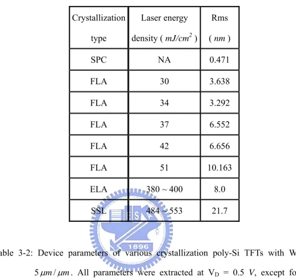
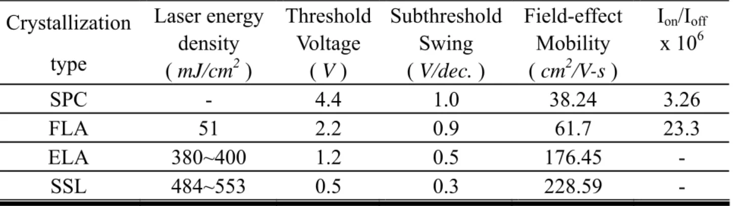
(10) Table Captions. Table 3-1. The roughness of various crystallization poly-Si thin films. Table 3-2. Device parameters of various crystallization poly-Si TFTs with W/L = 5 µm / µm . All parameters were extracted at VD = 0.5 V, except for the On/Off current ratio (Ion/Ioff) which were extracted at VD = 4.5 V. Table 3-3. Optimal device parameters of various crystallization poly-Si TFTs with W/L = 5 µm / µm . All parameters were extracted at VD = 0.5 V, except for the On/Off current ratio (Ion/Ioff) which were extracted at VD = 4.5 V. Table 3-4. Deep state density, subthreshold swing, oxide capacitance and substrate capacitance of various crystallization poly-Si TFTs were obtained from high-frequency measurement (1 MHz).. viii.
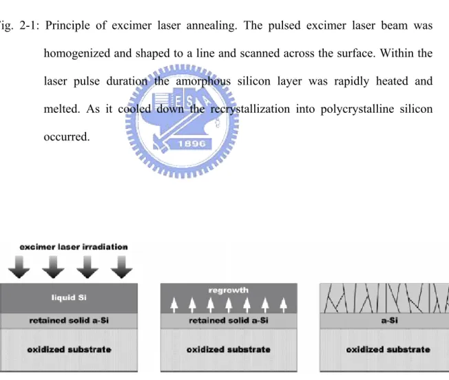
(11) Figure Captions. Chapter 2. Fig. 2-1. Principle of excimer laser annealing. The pulsed excimer laser beam was homogenized and shaped to a line and scanned across the surface. Within the laser pulse duration the amorphous silicon layer was rapidly heated and melted. As it cooled down the recrystallization into polycrystalline silicon occurred.. Fig. 2-2. The schematic view of the recrystallization mechanism in the partial melting regime.. Fig. 2-3. The schematic view of the recrystallization mechanism in the full melting regime.. Fig. 2-4. The schematic illustration of the recrystallization mechanism in the super lateral growth (SLG) regime.. Fig. 2-5. Illustration diagram to describe the crystallization mechanism with three regions and two specific energies.. Fig. 2-6. Timescales of various electron and lattice processes in laser-excited solids. Each green bar represents an approximate range of characteristic times over a range of carrier densities from 1017 to 1022 cm-3. The triangles at the top show the current state-of-the-art in the generation of short pulses of electromagnetic radiation: 1 5 fs (visible), 2 120 fs (X-ray), 3 0.5 fs (far ultraviolet) [30,48].. Fig. 2-7. Schematic the key process for device fabrication of poly-Si thin film transistors with solid-phase crystallization (SPC) and femtosecond laser annealing (FLA) structure.. ix.
(12) Fig. 2-8. Schematic cross sectional view of SPC and FLA poly-Si TFT with a conventional top-gate, coplanar, self-aligned structure.. Chapter 3. Fig. 3-1. The SEM images after secco etching of 100 nm thick a-Si annealed by SPC and FLA. FLA irradiated with 50 fs pulses, laser pulses fluence about 30 ~ 51 mJ/cm2 and an interpulse overlapping of 95% (20 laser shots).. Fig. 3-2. The SEM images after secco etching of 100 nm thick a-Si annealed by SPC. The maximum grain size of long axis was about 400 nm.. Fig. 3-3. The SEM images after secco etching of 100 nm thick a-Si annealed by FLA that irradiated with 50 fs pulses, laser pulses fluence about 30 mJ/cm2 and an interpulse overlapping of 95% (20 laser shots).. Fig. 3-4. The SEM images after secco etching of 100 nm thick a-Si annealed by FLA that irradiated with 50 fs pulses, laser pulses fluence about 34 mJ/cm2 and an interpulse overlapping of 95% (20 laser shots).. Fig. 3-5. The SEM images after secco etching of 100 nm thick a-Si annealed by FLA that irradiated with 50 fs pulses, laser pulses fluence about 37 mJ/cm2 and an interpulse overlapping of 95% (20 laser shots).. Fig. 3-6. The SEM images after secco etching of 100 nm thick a-Si annealed by FLA that irradiated with 50 fs pulses, laser pulses fluence about 42 mJ/cm2 and an interpulse overlapping of 95% (20 laser shots).. Fig. 3-7. The SEM images after secco etching of 100 nm thick a-Si annealed by FLA that irradiated with 50 fs pulses, laser pulses fluence about 51 mJ/cm2 and an interpulse overlapping of 95% (20 laser shots).. Fig. 3-8. Average grain size of SPC and FLA poly-Si films. FLA poly-Si films were. x.
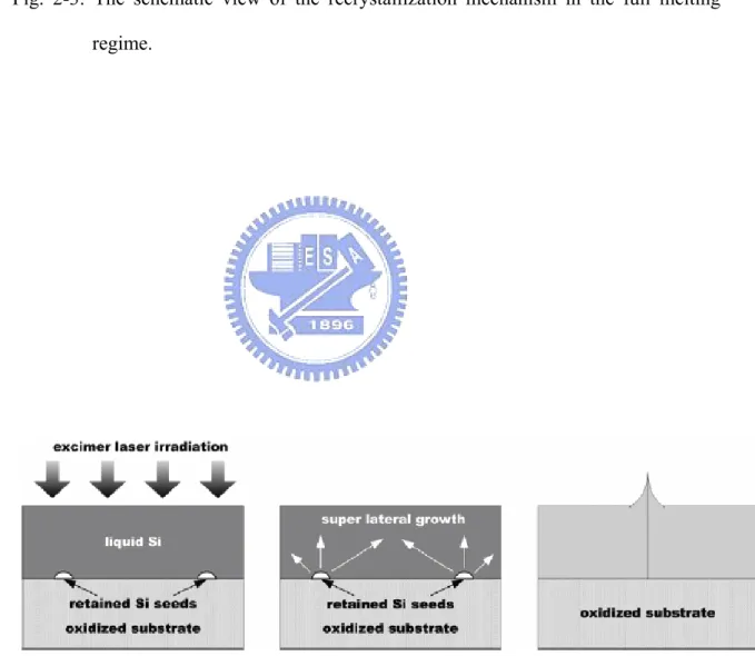
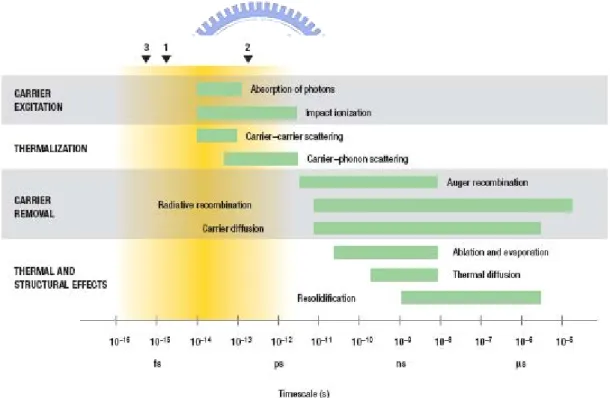
(13) irradiated by 50 fs laser pulses and laser energy density varied from 30 to 51 mJ/cm2. The SPC_W represented the short axis of SPC grain size and the SPC_L represented the long axis of SPC grain size. Fig. 3-9. The SEM images after secco etching of 50 nm thick Si annealed by ELA and SSL at each process laser energy density. (a) ELA (380 ~ 400 mJ/cm2) (b) SSL (484 ~ 553 mJ/cm2). Fig. 3-10. AFM images comparisons of SPC and FLA poly-Si thin films. FLA irradiated with 50 fs pulses, laser pulses fluence about 30 ~ 51 mJ/cm2 and an interpulse overlapping of 95% (20 laser shots).. Fig. 3-11. The roughness of various crystallization poly-Si thin films.. Fig. 3-12. The threshold voltage variation of SPC and FLA poly-Si TFTs.. Fig. 3-13. The field-effect mobility variation of SPC and FLA poly-Si TFTs.. Fig. 3-14. The typical transfer characteristics of poly-Si TFTs crystallized by SPC method.. Fig. 3-15. The output characteristics of poly-Si TFTs crystallized by SPC method.. Fig. 3-16. The typical transfer characteristics of poly-Si TFTs crystallized by FLA method. The laser energy density of FLA varied from 30 to 51 mJ/cm2.. Fig. 3-17. The output characteristics of poly-Si TFTs crystallized by FLA method. The laser energy density of FLA varied from 30 to 51 mJ/cm2.. Fig. 3-18. The typical transfer characteristics of poly-Si TFTs crystallized by SPC and optimal FLA condition.. Fig. 3-19. The output characteristics of poly-Si TFTs crystallized by SPC and optimal FLA condition.. Fig. 3-20 Comparison of typical transfer characteristic for n-channel poly-Si TFTs annealed by ELA (380 ~ 400 mJ/cm2) and SSL (484 ~ 553 mJ/cm2). Fig. 3-21. The deep state traps density of various crystallization poly-Si TFTs. FLA. xi.
(14) irradiated with 50 fs pulses, laser pulses fluence about 30 ~ 51 mJ/cm2. Fig. 3-22. The measured activation energy versus gate voltage plots of various SPC and FLA poly-Si TFTs.. Fig. 3-23. The band bending along the x axis at the SiO2 and poly-Si interface of an n-channel poly-Si TFT under a positive gate voltage.. Fig. 3-24. The trap state distribution included the bulk traps and the interface traps. It was modeled by the sum of a deep-level Gaussian distribution with a maximum at energy Etd near the midgap, an exponential-like band tail Ett and an exponential-like interface traps Eit both near the conduction-band edge.. Fig. 3-25. The trap state distribution of various SPC poly-Si TFTs with W/L = 5 µm / µm . Here SPC1,2,3 were different area of device.. Fig. 3-26. The trap state distribution of various laser energy density of FLA poly-Si TFTs with W/L = 5 µm / µm .. Fig. 3-27. The trap state distribution in deep state of SPC and various laser energy density of FLA poly-Si TFTs with W/L = 5 µm / µm .. Fig. 3-28. The trap state distribution in tail state and correspond with field-effect mobility of SPC and various laser energy density of FLA poly-Si TFTs. We defined the Nt(E) near conduction band was 1.15 eV.. Fig. 3-29. The trap state distribution through out the upper bandgap for poly-Si TFTs crystallized by various technologies.. Fig. 3-30 The C-V measurement plots of optimal SPC poly-Si TFTs with channel width of 100 um and length of 50 um. The measured frequency was varied from 50 kHz to 1 MHz. Fig. 3-31 The C-V measurement plots of FLA (42 mJ/cm2) poly-Si TFTs with channel width of 100 um and length of 50 um. The measured frequency was varied. xii.
(15) from 50 kHz to 1 MHz. Fig. 3-32. The C-V measurement plots of SSL poly-Si TFTs with W/L = 600/6 µm / µm . The measured frequency was varied from 50 kHz to 1 MHz.. Fig. 3-33. The C-V measurement plots of ELA poly-Si TFTs with W/L = 600/10 µm / µm . The measured frequency was varied from 10 kHz to 1 MHz.. xiii.
(16) Chapter 1 Introduction. 1.1 Overview of polysilicon thin-film transistors technology. In recent years, polycrystalline silicon thin-film transistors (poly-Si TFTs) have attracted more and more attention because of their widely applications in active matrix liquid crystal displays (AMLCDs) [1-3], and organic light-emitting displays (OLEDs) [4]. Except large area displays, poly-Si TFTs also have been applied into some memory devices such as dynamic random access memories (DRAMs) [5], static random access memories (SRAMs) [6], electrical programming read only memories (EPROMs) [7], and electrical erasable programming read only memories (EEPROMs) [8]. In addtion, several linear image sensors [9], thermal printer heads [10], photo-detector amplifier [11], and three dimension LSIs [12] have also adopted poly-Si TFTs technology. Among these, AMLCDs are the most primary application of poly-Si TFTs and lead extensively rapid development in poly-Si TFTs. Unlike amorphous silicon (a-Si) TFTs, poly-Si TFTs have much larger carrier mobility which usually exceeds 100 cm2 / Vs by present mature technology. Its superior carrier mobility is essential to successfully integrate polys-Si TFTs and peripheral driving circuits [5] on the same panel to reduce the assembly complexity and cost. Therefore, the low process temperature of poly-Si TFTs with the high mobility makes it possible to realize the ultimate goal, system-on-panel [13]. Furthermore, due to the higher mobility of poly-Si TFTs, the dimension of the poly-Si TFTs can be made smaller than that of a-Si TFTs to achieve high density and high resolution AMLCDs. However, there are still some problems existed in poly-Si TFTs. Compared to. 1.
(17) single crystalline silicon, poly-Si has a lot of defects at the grain boundaries. These defects, regarding as trap states, locate in the disordered grain boundary region and degrade device performance severely. In other words, the performances of poly-Si TFTs are strongly affected by the grain structure inside the channel region. Thus, the larger grain with less grain boundary defects is desirable and currently many researches attempting to achieve this goal have been studied, such as solid-phase crystallization (SPC) [14], excimer laser annealing (ELA) and solid state laser annealing (SSL). As a result, one of the major barriers in developing the technology lies in the growth of poly-Si grains with high uniformity and large grain size at the same time. In summary, the poly-Si TFTs will play an important role in many aspects in the future, especially as the three-dimensional circuit era is coming.. 1.2 Crystallization of Amorphous Silicon Thin Films. Because crystallization plays a dominant role in determining mobility and uniformity of the polysilicon material, a robust crystallization process is required for LTPS TFTs to become a mainstream technology. In polycrystalline material, grain boundaries cause trap and tail states which exert a negative influence on nearly all aspects of device performance including an increase in Vth, a decrease in subthreshold slope, a decrease in mobility, an increase in leakage current, and poor device stability [15]. The origin of the trapping states at the grain boundaries is though to be associated with the presence of dangling and strained bounds [16]. In general, the more grain boundaries there are in active-channel region, the poorer the device performance. Reduction of defect density in polycrystalline material will make it approach the quality of single-crystalline material, which will lead to better performance of polycrystalline device. Therefore, it is important to control as mush as possible the size of the grains,. 2.
(18) the number of the grains, and the location of the grains. Poly-Si thin films can be directly deposited on glass substrate by low-pressure chemical vapor deposition (LPCVD) [17-18] and electron cyclotron resonance chemical vapor deposition (ECRCVD). However, due to the high deposition temperature (approximately 625°C) and the poor crystallinity of the as-deposited poly-Si thin film, the direct deposition method has been excluded in the fabrication of LTPS TFTs. Several crystallization technologies for fabricating high quality poly-Si thin films have been widely studies. In general, we can classify the crystallization technique of poly-Si thin films simply into two groups: solid phase crystallization and liquid phase crystallization. In the solid phase crystallization, nucleation and grain growth are driven by thermal annealing [19]. It usually takes a long time to anneal a-Si thin film at low temperature. On the other hand, several kinds of laser equipments are adopted to crystallize the a-Si thin film [20-25]. During laser irradiation, the a-Si thin films are heated to the melting point and intermediately quench to the ambient temperature. Critical parameters for crystallization include grain size, grain size uniformity, number and location of the grains, laser energy stability, process temperature, resulting film thickness uniformity, throughput, and mobility. In the follow sections, several widely-used recrystallization methods are briefly reviewed. They include solid-phase crystallization (SPC), excimer laser annealing (ELA), solid state laser annealing (SSL) and femtosecond laser annealing (FLA).. 1.3 Motivation. High-performance silicon devices on thin film transistors (TFTs) have recently been incorporated in various applications, such as active matrix liquid crystal displays (AMLCD) and TFTs array. The key component for realizing such systems was low. 3.
(19) temperature. polycrystalline. silicon. (LTPS). thin-film. transistors. (TFTs).. Low-thermal-budget techniques, such as solid-phase crystallization (SPC), excimer laser annealing (ELA) [26-28] and solid state laser (SSL) annealing were commonly employed to crystallize the channel regions of LTPS-TFTs. In particular, efficient absorption of ultraviolet (UV) laser irradiation by amorphous silicon (a-Si) resulted in high-quality polycrystalline silicon (poly-Si) by excimer laser annealing (ELA). Unlike annealing using continuous-wave (cw) [29] and long pulse lasers, nonlinear photoenergy absorption and nonequilibrium thermodynamics were expected to dominate the interactions between the intense femtosecond laser pulses and irradiated transparent materials [30-35]. Such a nonlinear process provideed precise and low-threshold fluence associated with femtosecond laser ablation [32-36]. Then we studied the structural characteristics of recrystallized amorphous silicon films. At last we tried to make comparisons with near-infrared femtosecond laser annealing (FLA) and solid-phase crystallization (SPC) to accompany the device process. We reported infrared femtosecond laser-induced crystallization of amorphous silicon with high crystallinity at each lower laser energy density. Finally, the performance of poly-Si TFTs was strongly affected by the grain structure and the defect state distribution in the poly-Si film. In this thesis, different kinds of crystallization technologies were used. Their influences on device electrical characteristics were investigated.. 1.4 Thesis Outline. This thesis was organized into the following manner. In chapter 1, a brief overview of polysilicon thin-film transistors technology for various kinds of applications was introduced. Then we would describe several popular. 4.
(20) laser crystallization technologies because they seem to be very promising to fulfill low temperature polycrystalline silicon (LTPS). Finally, the motivation of this work would be expressed. In the beginning of chapter 2, various laser annealing system were given in detail in four kinds of methods. In addition, several thin film characterizing techniques containing material and electrical aspects were described. We also showed our device fabrication and process flow. Then we introduced the methods to measure or extract the typical parameters including threshold voltage, subthreshold swing, on/off current ratio and field-effect mobility. In chapter 3, first we analyzed the SEM and AFM images of various crystallization technologies poly-Si TFTs thin films. And we discussed with the device performances of various crystallization technologies poly-Si TFTs. Then we from the I-V measurement to analyze the deep state density, tail state density and the interface traps density. Finally by means of the C-V measurement under different frequency, we tried to extract the effective interface capacitance by equivalent circuit. In chapter 4 and chapter 5, the conclusions and future work were also given.. 5.
(21) Chapter 2 Fabrication process and device characterization. 2.1 Laser annealing system. 2.1.1 Heat transport and grain growth mechanism of Solid-Phase Crystallization (SPC) of amorphous-silicon. Solid-phase crystallization (SPC) of amorphous silicon (a-Si) is a simple and effective method to acquire poly-Si thin film with large grains. In the SPC furnace annealing, the a-Si thin film is annealed in a furnace at temperature as high as 600℃ for 24 hours. Amorphous silicon is a thermodynamically metastable phase, processing a driving force for transformation to polycrystalline phase given sufficient energy to overcome the initial energy barrier. Unfortunately, SPC using low-temperature furnace annealing requires very long anneal times and hence suffers from a substantial trade-off between performance and throughput [37]. The crystallization from an amorphous phase to a polycrystalline phase occurs through two processes—nucleation and grain growth [37]. Both of them have characteristic activation energies. The nucleation activation energy is extracted from the time to onset of crystallization, while the grain growth rate is extracted from grain progression data of about 5 eV. The rate of the crystal growth has an activation energy of about 2.7 eV. The nucleation activation energy is larger than the grain growth activation energy for the SPC system [38]. To achieve the largest possible grains, it is desirable to suppress nucleation relative to grain growth. Therefore, SPC is typically done at a low temperature. This results in a reduction in throughput through an increase. 6.
(22) in the incubation time and a decrease in the grain growth rate. Higher temperatures increase throughput oppositely. However, excessive nucleation results in smaller grains and hence poorer performance. Deposition rate also affects the structural order of the as-deposited film. Amorphous-Si thin films deposited at higher rates have higher structural disorder which results in lower nucleation rate during crystallization and thus larger grain size. Therefore, crystallization of a-Si thin films deposited by thermal decomposition of disilane yield very large grain size. Thus SPC can be accomplished within a wide annealing temperature range that requires a similar wide range of annealing time (i.e. time required for complete transformation of the precursor-Si film to poly-Si). The relationship between annealing temperature and annealing time is not unique. Based on the above transformation method, large grain size relates to longer crystallization time. For practical applications, the crystallization time corresponding to average grain size exceeding 0.5-1 µm may be prohibitingly long. The typical SPC poly-Si microstructure is characterized by a large density of structural defects. The result of this high grain-defect density is a saturation in the electrical performance of poly-Si TFTs, fabricated with such poly-Si films with grain size larger than approximately 0.3-0.5 µm. Therefore, standard SPC technology can only produce poly-Si TFTs of mediocre performance. This translated to a mobility range 20 - 40 cm2 / Vs and the threshold voltage ranges from 3 to 6 V. Despite of the mediocre performance, solid-phase crystallization (SPC) is a promising technique due to its simplicity, low cost, and excellent uniformity [39].. 2.1.2 Heat transport and grain growth mechanism of Excimer Laser Annealing (ELA) of amorphous-silicon. Excimer laser crystallization (ELC) of a-Si thin film is presently widely used. 7.
(23) method for preparing poly-Si thin film on foreign substrates. Excimer lasers emit in the UV region (output wavelengths 193, 248, and 308 nm for ArF, KrF and XeCl gas mixtures, respectively) with a short pulse duration (10-30 ns). The combination of strong optical absorption of the UV light in silicon ( α > 106 cm-1) and small heat diffusion length during the laser pulse ( ~ 100 nm) implies that high temperature can be produced in the silicon surface region, causing melting, without appreciable heating of the substrate. This makes the ELC process compatible with glass or plastic substrate, one of the major advantages of this technique. There are many discussions in the literature of the absorption mechanism of intense laser radiation in solids. Among them, four absorption mechanisms in semiconductors seem to be important. They are: (1) Direct excitation of lattice vibrations by absorption of light with photon energy (hν) well below the band-gap energy (Eg). (2) Excitation free or nearly free carriers by absorption of light with hν < Eg; such carriers will always be present as a result of finite temperatures and/or doping. (3) An induced metallic mechanism due to free carriers generated by the laser light itself. (4) Electron-hole excitation by light with hν < Eg. Excimer laser annealing (ELA) systems use Long beam homogenizer to make excimer laser beam’s energy duration the amorphous silicon film for uniform annealing results. Excimer lasers have typically a rectangular beam profile, whereas the long axis has a top head and the short axis has a Gaussian like shape [40]. In LPTS-TFT laser annealing process the laser beam is formed to a line shape. This modified beam with an adjustable width between 0.1 and 1.0 mm and a length of up to 370 mm is scanned over the amorphous silicon (see Fig. 2-1). For increasing display size lasers with higher output power are required in order to achieve sufficient laser. 8.
(24) energy density on the target. The recent high power excimer lasers for silicon annealing deliver 300 W (i.e. 1 Joule at 300 Hz) [40]. Kuriyama et al. used thermal analysis to calculate the recrystallization process during ELC [41], [42]. The solidification velocity of molten Si during laser annealing can be controlled by three factors: laser pulse width, laser energy density, and substrate temperature during ELC. According to their papers, the substrate temperature is most effective among the three factors. The melting duration increases with substrate temperature. The solidification velocity can be reduced to about one-third by substrate heating. It is becoming increasing clear that the excimer laser-induced phase and structural modifications of thin Si films involve several melt-mediated and far-from equilibrium transformation process. J. S. Im et al. identified that excimer laser crystallization of a-Si thin film on foreign substrates can divide into three transformation regimes with respect to the applied laser energy densities [43], [44]. They are partial melting regime, fully melting regime, and near complete melting regime as shown in Fig. 2-2 ~ Fig. 2-4 respectively.. Partial-melting regime (low energy density regime). In the partial melting regime, the energy density of incident laser pulse is above the surface melting threshold but below the complete melt-through energy density (i.e., melting depth < film thickness). The a-Si thin film can be partially melted and subsequently can be crystallized. Explosive crystallization of a-Si thin film occurs at the onset of the transformation and follows by vertical regrowth. The early trigger of explosive crystallization may be attributed either to the presence of microcrystalline clusters – which was confirmed by analyzing the solid-phase crystallization behavior. 9.
(25) and is absent in high-dose ion irradiated a-Si thin films – and/or to the possible presence of impurities such as hydrogen. In this regime, there is an increase in the grain size with increases in the laser energy density. This occurs up to the point at which the average grain radius is approximately equal to the film thickness.. Complete melting regime (high energy density regime). In the complete melting regime, the energy density of incident laser pulse is sufficient high to lead to a complete melting of the a-Si thin film and no unmelted Si remains. A sudden increase in the melt duration, which is observed at the transition from the low to high energy density regime, is strong indicative of the transition from partial melting and regrowth to complete melting. The complete-melting Si thin film is then followed by significant supercooling of the liquid before the occurrence of the transformation to the solid phase. In this regime, the final microstructure is insensitive to large variations in laser energy densities. For low substrate temperature, fine-grained and small-grained poly-Si thin films are observed. In addition, amorphization of the poly-Si thin film is found for thinner film thickness.. Near complete melting regime (super lateral growth regime). In the near complete melting regime, the energy density of the incident laser pulse leads to an unmelted a-Si thin film composed of discrete islands (i.e. melting depth ≅ film thickness). At this point, with a small increase in the energy density, an extremely sharp increase in the grain size occurs. Due to the technological significance of large-grained poly-Si thin film and its dramatic nature, this regime is also referred as the. 10.
(26) super lateral growth (SLG) regime. With further slight increases in laser energy density, a dramatic reversal in the microstructural trend is observed in that fine-grained poly-Si thin film is obtained. This transition marks the end of the low energy density regime and the beginning of the high energy density regime. In view of the above interpretations imposed on the low and high energy density regimes, it can be argued that the large-grained poly-Si thin film obtained in the SLG regime is a consequence of the liquid phase regrowth from the discontinuous and small solid seeds, which are never fully melted. In other word, the SLG regime corresponds to the condition at which point near-complete melting of the film occurs to the extent that the unmelted a-Si thin film no longer forms a continuous layer; instead, the residual Si is composed of discrete island. Hence, as the temperature begins to drop, growth from these clusters can proceed. Depending on the separation distance between these seeds, it is possible for significant lateral growth to take place before the impingement of the grain occurs. However, there is a limit to the maximum lateral growth distance, which can be achieved as continuous cooling of the liquid layer via conduction to the substrate eventually would lead to copious nucleation of solids in bulk liquid ahead of the interface. High substrate temperature lead to lower quenching rates, which in turn provides more time for lateral growth to take place before bulk nucleation intervenes. In addition, the SLG distance will also increase with increasing film thickness, decreasing thermal conductive of the substrate, and increasing the laser pulse duration [44].. 2.1.3 Heat transport and grain growth mechanism of Solid State Laser annealing (SSL) of amorphous-silicon. Compared to the ELA technology, solid state laser annealing (SSL) with Nd:YAG laser source have advantages such as stable laser power and low maintenance fee on. 11.
(27) AMLCD mass production applications. Many researches have been proposed to use the 2nd harmonic wave of Nd:YAG laser (532 nm wavelength) to crystallize the a-Si film [45-47]. Most papers discuss the large lateral grains produced by low-power continuous-wave Nd:YAG laser [45-47]. However, rectangular grain size causes device deviation when different current flow directions are designed on the same substrate. To overcome these problems, high power Nd-YAG pulsed laser is proposed. SSL with high power (up to 175 W ) Nd:YAG (2ω) laser source, long line beam with beam length as 105 mm can be produced. In the sort-axis direction, the beam profile had Gaussian-like energy distribution with the Full Width at Half Maximum (FWHM) as 40 µm. Its Gaussian-like beam profile was a great advantage because it was much easier to induce lateral crystallization compared to typical ELA system. Besides, the scan pitch can be varied from 1 µm (overlap 97.5%) to 30 µm with repetition rate as 4 kHz. Although the beam size of SSL was much smaller than ELA, its high repetition rate can make the throughput to be comparable to ELA in mass production. When mentioned the crystallization mechanism, we can propose three regions in the crystalline one. As illustrated in Fig. 2-5, three regions named vertical crystallization (VC), super lateral crystallization (SLG) and fine grain (FG) regions are divided by two specific laser energy. The first is the critical energy (Ec) that stands for the laser energy to fully melt the a-Si film. The second is the fine-grain energy (Efg) that stands for the minimum energy to cause the fine grain structure. Three regions will be further described as follows. In regionⅠ, the laser energy is not high enough to completely melt the a-Si film. As a result, the nucleation sites are located at the boundary between melted Si film and the bulk a-Si film. Vertical growth dominates the crystallization mechanism and gives rise to small grain structure. The grain size increases as the melted zone increases along with increasing laser energy density. The scan pitch also influences the grain size in this. 12.
(28) VC region. When the scan pitch decreases, the grain size becomes larger. This is due to the increase of laser beam overlap and also the increase of melted Si zone. In other words, the absorbed energy per unit area of the Si film is increased when the scan pitch decreases. In region Ⅱ, named the SLG region, grain size becomes large when the laser energy exceeds the critical energy (Ec). In this region, a-Si film is fully melted. Nucleation happens at the cooling boundary produced by the Gaussian-distributed laser beam profile. Super lateral crystallization dominates the crystal mechanism. In this region, the grain size is not dependent on the laser energy obviously. It is plausible that reducing the beam profile slope can further increase the grain size. However the verification is still beyond our facility. This corresponds to the proposed critical energy concept that causes the a-Si film fully-melted. In region Ⅲ, the laser energy exceeds the second specific laser energy which is the fine grain energy (Efg). Fine grain areas next to the large grain areas start to appear. We will see in the later discussion about device performance that the fine grain areas degrade device performance tremendously whereas the existence of large grain areas. Since the slope of the Gaussian profile increases when we enlarge the peak laser energy. It is plausible that the fine grain areas are caused by the large cooling rate. Large cooling rate produces areas where temperature variation is very large. In these specific areas, many nucleation sites appear simultaneously and form the fine grain structure.. 2.1.4 Femtosecond Laser Annealing (FLA) system. Femtosecond laser pulses impart extremely high intensities and provide precise laser-ablation thresholds at substantially reduced laser energy densities. Femtosecond laser induced phase transitions in covalently bonded semiconductors have been. 13.
(29) extensively studied during the past decade. On excitation with a femtosecond pulse, a semiconductor undergoes several stages of relaxation before returning to equilibrium. The energy is transferred first to the electrons and then to the lattice. The interaction includes several regimes of carrier excitation and relaxation. We can distinguish the following four regimes: (1) carrier excitation, (2) thermalization, (3) carrier removal and (4) thermal and structural effects [48]. These regimes and the timescales for the corresponding processes are shown in Fig. 2-6.The triangles at the top of the figure mark the current state-of-the-art in the generation of ultrashort pulses of various wavelengths. In the visible region, pulses as short as 5 fs allow direct probing of carrier dynamics down to the shortest timescales (triangle 1). Diffraction of hard X-ray pulses of 200 fs duration (triangle 2) permit observation of structural and atomic rearrangements in the bulk of materials, but not the carrier excitation and carrier–lattice interaction processes that precede the structural dynamics, because X-rays cannot see electrons. The shortest pulses obtained to date, of 800 as duration (triangle 3), are in the soft X-ray region, and are limited to probing corelevel transitions in excited atoms [30]. For picosecond and subpicosecond laser pulses, however, ample experimental evidence exists from Shank and co-workers [49] and other groups, that nonthermal structural changes can be driven directly by electronic excitation [50]. According to the so-called non-thermal plasma model, the lattice is disordered by direct excitation of the electronic system, while the lattice modes remain vibrationally cold. Absorption of photons creates a free carrier plasma and, when about 10% of valence electrons are removed from bonding orbitals, the lattice is weakened. Photoexcitation can thus give the atoms enhanced mobility without increasing their thermal energy. The non-thermal model assumes that the rate of phonon emission by the excited electronic system is slow compared with the laser pulse duration. When this assumption is satisfied, and a large. 14.
(30) enough fraction of the valence electrons is excited, structural change can occur while the electronic system and the lattice are not in thermal equilibrium with each other, although each of these systems may internally be in quasi-equilibrium [48]. Mechanisms of femtosecond laser-induced ablation on crystalline silicon are investigated by time-resolved pump-and-probe microscopy in normal imaging and shadowgraph arrangements. The imaging with the time-delayed frequency-doubled probe beam had a temporal resolution of 100 fs. The high electron temperatures and dense solid state plasma formation suggest a non-equilibrium phase transition process. Thermionic emission and photoemission of electrons can initiate air plasma in the proximity of the surface. Time-resolved shadowgraphs of the shock wave propagation show that the ultrafast initial plasma becomes visible at around 10 ps and is followed by a slower ‘‘thermal’’ contribution in the time scale of 30 ns. The instantaneous energy released upon initiation of explosion is estimated to be 10%–17% of the absorbed laser energy depending on the incident laser energy. The pressure of the released shock wave was calculated to be about a few hundreds of atm [33]. The intense femtosecond laser pulses lead to efficient nonlinear photon adsorption in irradiated materials, enabling a melting of amorphous silicon films. Femtosecond laser annealing (FLA) assisted by a scanning of the laser beam efficiently crystallizes amorphous silicon films with large grains, using a total laser energy as low as ~ 0.9 J /cm2 [36]. The results of near-infrared femtosecond laser annealing are described in section §3.2. Then the comparisons between near-infrared femtosecond laser annealing and solid-phase crystallization is also given. Up to now, a clear distinction of the transition between the ultrafast liquid phase and the electron-hole plasma state is hard. However, it is undoubted that the classical thermal model of crystallization mediated cannot explain the subpicosecond rapid phase transition satisfactorily.. 15.
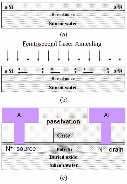
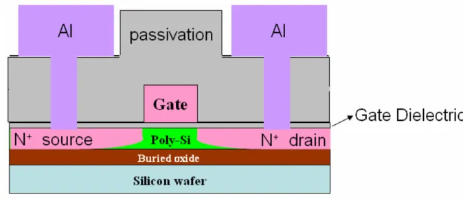
(31) 2.2 Device fabrication. In this experiment, we fabricate the poly-Si TFTs with a typical structure of top-gate, coplanar self-aligned TFT. The process flow and the schematic cross sectional view of the devices were shown in Fig. 2-7 and Fig. 2-8. The fabrication procedure is described as follows.. Step1. Substrate. 6-inch p-type single crystal silicon wafers with (100) orientation were used as the starting materials. After an RCA initial cleaning procedure, Si wafers were deposited with 550nm-thick thermally grown SiO2 as the buried oxide in steam oxygen ambient at 980°C. Step2. Active region formation (Mask1). Undoped 100 nm thick amorphous-Si layer were deposited by low-pressure chemical vapor deposition (LPCVD) on buried oxide by pyrolysis of silane (SiH4) at 550°C. The amorphous-Si films were recrystallized by solid-phase crystallization (SPC) method at 600°C for 24hrs in an N2 ambient for a part of Si wafers as the comparison. And the others as the femtosecond laser annealing (FLA) experimentation were recrystallized using an infrared femtosecond Ti: sapphire laser system (TSUNAMI, and SPIT FIRE, from the Spectra-Physics Company) with a wavelength of 800 nm, a repetition rate of 1 kHz, a pulse duration of 50 fs, and a total laser energy as low as ~ 1.02 J /cm2, all samples were placed in a vacuum chamber, and a heater increased the substrate temperature up to 400°C. Then the recrystallized poly-Si films were patterned into the active islands (Mask1), including source, drain and channel with different dimension by lithography. 16.
(32) equipments (Track and G-line stepper) and transformer couple plasma (TCP poly etcher) etching using the mixture of Cl2 and HBr. Step3. Gate oxide formation. In order to decrease the roughness of interface between the gate oxide and poly-Si islands, thermal oxidation of silicon is excluded. After defining the active region, the wafers were boiled in H2SO4 + H2O2 to ensure cleanliness of the wafers before deposition. A buffered HF dip was performed to remove the native oxide on the silicon surface. Soon, the gate insulator was deposited in a horizontal furnace using TEOS and O2 gases at 700°C. The thickness of the TEOS oxide thin film is 50 nm. Step4. Gate electrode formation (Mask2). After deposition of the gate insulator, 150 nm poly-Si films were deposited immediately on the gate insulator by LPCVD at 620°C. The poly-Si layer were then patterned by Track and G-line stepper and transformer couple plasma (TCP poly etcher) etching to define the gate electrode and to be the mask for self-aligned implantation. Step5. Self-aligned offset source/drain formation. After Mask2 process, phosphorus ions at a dose of 5×1015 cm-2 were implanted to form the n+ gate and source/drain regions and the self-aligned offset regions in the same process step. Step6. Passivation layer and contact hole formation (Mask3). After implanted the source/drain regions, we etched the gate insulator and deposited 300 nm thick TEOS oxide as the passivation layer to protect TFTs by LPCVD at 700°C. Then define the contact hole. Dopants were activated by rapid thermal annealing (RTA) for spike anneal at 1050ºC and duration time 0.2 sec. Step7. Metallization. The 500 nm thick aluminum (Al) layer were deposited by metal-physical vapor. 17.
(33) deposition (Metal PVD) and then patterned for the source/drain and gate regions as the metal pads. Finally, the finished devices were sintered at 400°C for 30 minutes in an N2 ambient.. 2.3 Material analysis of thin film structure. In this section, we briefly introduced several experimental techniques adopted in this work to characterize the material and electrical properties of thin film. In parallel to the device fabrication, thin film properties with various laser annealing conditions were first analyzed by atomic force microscopy (AFM) and scanning electron microscopy (SEM). The Root-mean-square (RMS) roughness of various crystallization technologies thin film were analyzed and the average grain size was determined by top view image of scanning electron microscopy (SEM) after secco etching. On the other hand, for device electrical performances, they were measured by HP 4156A semiconductor parameter analyzer and several important parameters were extracted from the measured data, such as threshold voltage, subthreshold swing, on/off current ratio, field-effect mobility and so on. Except I-V measurement, we also analyzed C-V characteristics of devices by HP 4284 in final sections.. 2.4 Methods of device parameter extraction. In this section, we will introduce the methods of typical parameters extraction such as threshold voltage (Vth), subthreshold swing (S.S.), On/Off current ratio (Ion/Ioff) and field-effect mobility (µFE) from device characteristics.. 18.
(34) 2.4.1 Determination of the threshold voltage Plenty ways were used to determine the threshold voltage which was the most important parameter of semiconductor devices. Here, the method to determine the threshold voltage was the constant current method that the gate voltage at a specific drain current IN was considered as the threshold voltage. This method was adopted in most research of poly-Si TFTs. Compared to the threshold voltage obtained by the complex linear extrapolation method, it was more efficient to get the threshold voltage of the device and the value was close to the former one. In general, the threshold current IN = ID / (Weff / Leff) was specified at 10 nA for VD = 0.1 V (linear region) and 100 nA for VD = 5 V (saturation region) in most papers to extract the threshold voltage of TFTs.. 2.4.2 Determination of the Subthreshold Swing Subthreshold swing SS (V / dec.) was a typical parameter to describe the control ability of gate toward channel which was the turn on / off speed of a device. It was defined as the amount of gate voltage required to increase / decrease drain current by one order of magnitude. In this study, the subthreshold swing was defined as one-half of the gate voltage required to decrease the threshold current by two orders of magnitude (from 10-8A to 10-10A). The threshold current was specified to be the drain current when the gate voltage was equal to threshold voltage.. 2.4.3 Determination of On/Off Current Ratio Drain On/Off current ratio is another important factor of TFTs. High On/Off ratio represents not only large turn-on current but also small off current (leakage current). It affects gray levels (the bright to dark state number) of TFT AMLCD directly. There are many methods to specify the on and off current. The practical one is to. 19.
(35) define the maximum current as on current and the minimum leakage current as off current while drain voltage is applied at 4.5V.. 2.4.4 Determination of the field-effect mobility Typically, the field-effect mobility (µFE) was determined from the transconductance (gm) at low drain bias (Vd = 0.1V). The transfer I-V characteristics of poly-Si TFTs can be expressed as. I D = µ FE C OX. W 1 2 [(VG − Vth )VD − VD ] L 2. (2-1). Where COX is the gate oxide capacitance per unit area, W is channel width, L is channel length, Vth is the threshold voltage. If VD is much smaller than VG-Vth (i.e. VD << VG-Vth) and VG > Vth, the drain current can be approximated as: I D = µ FE C OX. W (VG − Vth )VD L. (2-2). The transconductance is defined as gm =. ∂I D |V =const . ∂VG D. (2-3). From Eq.(2-2), we find the transconductance to be gm =. W C OX µ FEV D L. (2-4). L gm C OX WVD. (2-5). Thus,. µ FE =. 20.
(36) Fig. 2-1: Principle of excimer laser annealing. The pulsed excimer laser beam was homogenized and shaped to a line and scanned across the surface. Within the laser pulse duration the amorphous silicon layer was rapidly heated and melted. As it cooled down the recrystallization into polycrystalline silicon occurred.. Fig. 2-2: The schematic view of the recrystallization mechanism in the partial melting regime.. 21.
(37) Fig. 2-3: The schematic view of the recrystallization mechanism in the full melting regime.. Fig. 2-4: The schematic illustration of the recrystallization mechanism in the super lateral growth (SLG) regime.. 22.
(38) Fig. 2-5: Illustration diagram to describe the crystallization mechanism with three regions and two specific energies.. Fig. 2-6: Timescales of various electron and lattice processes in laser-excited solids. Each green bar represents an approximate range of characteristic times over a range of carrier densities from 1017 to 1022 cm-3. The triangles at the top show the current state-of-the-art in the generation of short pulses of electromagnetic radiation: 1 5 fs (visible), 2 120 fs (X-ray), 3 0.5 fs (far ultraviolet) [30,48].. 23.
(39) Fig. 2-7: Schematic the key process for device fabrication of poly-Si thin film transistors with solid-phase crystallization (SPC) and femtosecond laser annealing (FLA) structure.. 24.
(40) Fig. 2-8: Schematic cross sectional view of SPC and FLA poly-Si TFT with a conventional top-gate, coplanar, self-aligned structure.. 25.
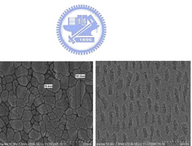
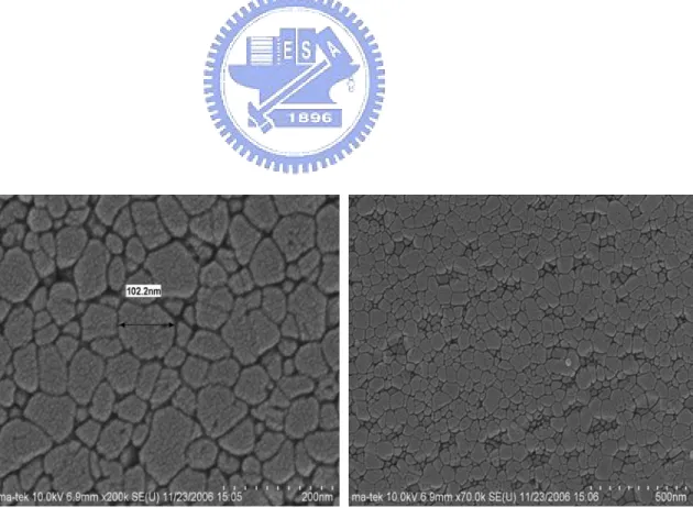
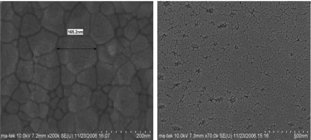
(41) Chapter 3 Results and Discussions. 3.1 Material characterization of various crystallization thin films. 3.1.1 SEM analysis (grain size) As mentioned in section 2.2, we deposited an undoped 100 nm thick amorphous-Si layer by low-pressure chemical vapor deposition (LPCVD) on buried oxide. Then the amorphous-Si films were recrystallized by solid-phase crystallization (SPC) and femtosecond laser annealing (FLA), respectively. After the processing and secco etching, we wanted to analyze the surface morphology of thin films by scanning electron microscopy (SEM). Fig. 3-1 showed the SEM images after secco etching of 100 nm thick a-Si annealed by SPC and FLA. The typical fabrication with SPC poly-Si films had a grain size larger than approximately 0.3 ~ 0.5 um. Therefore, standard SPC technology could only produce poly-Si TFTs of mediocre performance. Despite of the mediocre performance, SPC crystallization technology did offered a significant advantage in uniformity. Here we had an average grain size of 240 ~ 480 nm in Fig. 3-2 and Fig. 3-8 closing to the standard SPC technology. In the other hand, we represented line-scan FLA samples irradiated with a 95% interpulse overlapping (20 laser shots) of 50 fs laser pulses with different fluence of 30 ~ 51 mJ / cm2. At every laser fluence with its obvious SEM image had an optimal view and integral view in Fig. 3-3 to 3-7. We could find the relationships between the average grain sizes and the laser fluence. As the laser fluence increased, the average grain size gone up till reaching the maximum average grain sizes (about 114 nm and 165 nm). 26.
(42) when the laser fluence was 42 mJ / cm2 and 51 mJ / cm2. Between the laser fluence of 30 mJ / cm2 to 37 mJ / cm2, the grain structures and the average grain sizes (about 105 nm. to 120 nm) were very similar as shown in Fig. 3-8. Despite the difference between the mechanism of photoexcitation melting using FLA (Nonlinear annealing) [38-42] and that when using nanosecond or longer pulse laser annealing (linear annealing), such as ELA, lateral elongating still dominated the growth of grains in FLA poly-Si films. In these experiments, the maximum average grain size (~ 165 nm) of crystallized films, and the optimal laser fluence of crystallization (51 mJ / cm2) for FLA using 50 fs laser duration was markedly better than others. It was responsible that the grain sizes would depend on the efficiency of nonlinear photoenergy absorption [42],[43] in the same pulse duration and laser fluence. We also demonstrated the SEM images after secco etching of 50 nm thick a-Si thin films annealed by ELA (380 ~ 400 mJ/cm2) and SSL (484 ~ 553 mJ/cm2) at each process laser energy density in Fig. 3-9. And mentioned the crystallization technologies of ELA and SSL were not in our experiment at the same time. These two crystallization technologies were reached the commercialize fabrication and different from our lab experiment of SPC and FLA.. 3.1.2 AFM analysis (roughness) As shown in Fig. 3-10, the surface morphology and its roughness of poly-Si thin films crystallized by SPC and FLA were measured by atomic force microscopy (AFM). Compare to FLA thin films, the larger laser fluence (from 30 to 51 mJ / cm2) had a worse roughness (from 3.638 to 10.163 nm) as shown in Fig. 3-11 and Table 3-1. It was because the higher laser fluence caused the melted grain to pile up a higher grain boundary, even the stronger laser pulses would damage to form a nick over the crystallized a-Si thin films. But after we tried various laser fluences, the density of 51. 27.
(43) mJ / cm2 was the best condition to form a larger grain size than others. In addition, we. also found out the roughness of ELA and SSL poly-Si thin films about 8.0 nm and 21.7 nm. The roughness of ELA thin films was more uniform than the FLA of laser fluence. of 42 and 51 mJ / cm2 and the SSL thin films. The output characteristics of various crystallization technologies would be introduced at next section.. 3.2 Electrical characterization of various crystallization poly-Si TFTs. 3.2.1 Electrical characteristics of poly-Si TFTs crystallized by SPC method Standard SPC technology could only produce poly-Si TFTs of mediocre performance. This translated to a mobility range of 20 ~ 40 cm2 / Vs and a threshold voltage range of 3 ~ 6 V. Despite of the mediocre performance, SPC crystallization technology did offered a significant advantage in uniformity. Excellent mobility and threshold voltage uniformity had been reported for TFTs fabricated with poly-Si films crystallized by rapid-thermal-annealing. This meant that SPC process might be well suited to display applications that required intermediate-level, but highly repeatable, poly-Si TFT characteristics (i.e. AM-OLEDs). In this experiment the SPC poly-Si TFTs demonstrated a threshold voltage range of 4.1 ~ 4.57 V in Fig. 3-12. Owning a subthreshold swing range of 0.82 ~ 1.05 V / dec. and a field-effect mobility range of 38.24 ~ 45.78 cm2 / Vs in Fig. 3-13. And gaining an On/Off current ratio range of 1.9x10⁶ ~ 3.26x10⁶ in Table 3-2. The typical transfer and output characteristics were demonstrated in Fig. 3-14 and Fig. 3-15.. 3.2.2 Electrical characteristics of poly-Si TFTs crystallized by FLA method. 28.
(44) Different from SPC crystallization technology, near-infrared femtosecond laser annealing using intense ultrashot laser pulses led to efficient nonlinear photoenergy absorption and the generation of very dense photoexcited plasma in irradiated materials, enabling nonlinear melting on transparent silicon materials. FLA assisted by spatial scanning of laser strip spot constitutes superlateral epitaxy that could crystallize a-Si films with large grains. FLA experimentation was recrystallized using an infrared femtosecond Ti: sapphire laser system with a wavelength of 800 nm. The laser was used by a repetition rate of 1 kHz, a pulse duration of 50 fs (overlapping of 95%, 20 laser shots). And the total laser energy was as low as ~ 1.02 J /cm2. In this experiment the FLA poly-Si TFTs with the same channel width and length of 5 um, laser energy density from 30 to 51 mJ /cm2 displayed various electrical characteristics in Table 3-2. The typical transfer and output characteristics were demonstrated in Fig. 3-16 and Fig. 3-17. When the laser energy density was during 30 to 37 mJ /cm2, the electrical characteristics were similar with each other. It wes responsible that the grain sizes would depend on the efficiency of nonlinear photoenergy absorption in the same pulse duration and laser fluence. The average grain sizes of laser energy density of 42 and 51 mJ /cm2 were significant better than 30 to 37 mJ /cm2. We could also verify the difference from the Fig. 3-8. The threshold voltage. and field-effect mobility of the laser energy density of 42 and 51 mJ /cm2 were better than others, even ahead of SPC poly-Si TFTs as presented in Fig. 3-12 and Fig. 3-13.. 3.2.3 Electrical characteristics comparisons of optimal poly-Si TFTs crystallized by various crystallization methods We tried to find out the optimal poly-Si TFT crystallized by SPC and FLA methods and compared with each other. As shown in Table 3-3, the SPC poly-Si TFTs with the same channel width and length of 5 um. It demonstrated a threshold voltage of 4.4 V, a. 29.
(45) subthreshold swing of 1.0 V / dec., a field-effect mobility of 38.24 cm2 / Vs and an On/Off current ratio of 3.26x10⁶. The FLA poly-Si TFTs with the same channel width and length of 5 um. It demonstrated a threshold voltage of 2.2 V, a subthreshold swing of 0.9 V / dec., a field-effect mobility of 61.7 cm2 / Vs and an On/Off current ratio of 23.3x10⁶. As demonstrated in Fig. 3-18 and Fig. 3-19, the performance of the SPC poly-Si TFTs in this research was higher than the conventional SPC crystallization technology. It was due to the high quality in grain size and uniformity. Although the near-infrared FLA poly-Si TFTs of laser energy density of 51 mJ /cm2 had an excellent performance than all the others device, but the uniformity of grain size was not expected to come. Due to the pulse duration variation of peak power resulted in the stability and uniformity. We would like to improve the limitation of machinery and have an excellent performance of grain growth and uniformity. The optimal device parameters of ELA and SSL poly-Si TFTs were also demonstrated in Table 3-3. The optimal laser energy density of ELA was 380 ~ 400 mJ /cm2, and SSL was 484 ~ 553 mJ /cm2. The ELA poly-Si TFTs showed a threshold. voltage of 1.2 V, a subthreshold swing of 0.5 V / dec. and a field-effect mobility of 176 cm2 / Vs. The SSL poly-Si TFTs demonstrated a threshold voltage of 0.5 V, a. subthreshold swing of 0.3 V / dec. and a field-effect mobility of 229 cm2 / Vs. Because of these two crystallization technologies were commercialize fabrication in our collaboration with Auo corporation. And the comparison of typical transfer characteristic for n-channel poly-Si TFTs annealed by ELA and SSL at each best laser condition was also presented in Fig. 3-20.. 3.3 Defect analysis from I-V measurement. 30.
(46) 3.3.1 Defect analysis from subthreshold swing The thin film quality and defect analysis were conferred by introducing two independent methods. The HP4284A LCR meter was used to analyze the interface trap density. And base on the measured results, we analyzed the capacitance-voltage (C-V) characteristics of various crystallization poly-Si TFTs. The dimensions of SPC and FLA devices with channel width of 100 um and length of 50 um, SSL with 600 um / 6 um and ELA with 600 um / 10 um. The signal frequency is adjusted from 50 kHz to 1 MHz. After C-V measurement, a subthreshold swing to extract interface trap density method at a very high frequency was introduced as follows: [51] S≅. C kT ln 10 ⋅ (1 + D ) q Ci. (3-1) C D + C it Ci C 1+ D Ci. 1+ S with int erface traps ≡ S no int erface traps ×. (3-2). where CD = Cb and Cb is the depletion capacitance of device, Ci = Cox and Cox is the inversion capacitance of device. It is also given: Cb =. C ox C hf. (3-3). C ox − C hf. where Chf is the accumulation capacitance of device and there would be no capacitance induced by interface traps (Cit =0). Then from equation (3-2) and (3-3), we can transfer the equations as follows: Dit =. C ox qS C ( − 1) − b q 2.3kT q. (3-4). where Dit is the interface trap density at very high frequency of C-V measurement. After extraction and calculation, we can get various parameters comparison of various crystallization poly-Si TFTs as shown in Table 3-4 and Fig. 3-21. We noticed that the signal is operated at a very high frequency of 1 MHz. The interface trap density. 31.
(47) of the device fabricated through various crystallization methods was extracted by different subthreshold swing. Among of all, we found the interface trap density of the device fabricated by ELA is the lowest. The second one was SSL, then FLA got and the SPC owned a worst defect density compared to ELA and SPC. Actually, we could not to verify the accuracy of all. Then, the other method of defect analysis from activation energy was introduced and compared at next section.. 3.3.2 Defect analysis from activation energy Another defect analysis from I-V measurement was to extract the activation energy at different temperatures (from room temperature 25 up to 100℃) and gate voltages (from -5 to +25 V) with a source-drain voltage Vsd = 0.5 V. The devices had the same channel width and length of 5 um. Details of the fabrication process had been presented previously. An analytical expression for activation energy Ea was obtained for various models of bulk and interface states. Using a computer minimization program to fit the experimental Ea versus Vg data with the theory, the energy distribution of the bulk states and the interface states were separated for SPC and FLA poly-Si TFTs. A comparison of the calculated activation energy of various SPC and FLA poly-Si TFTs were shown in Fig. 3-22. We could find that the SPC had a small shift of gate voltage and an activation energy Ea of approximately 0.6 eV. At the same time, the FLA had almost no shift of gate voltage and the Ea higher than 0.6 eV when the laser energy density at 42 and 51 mJ/cm2. Therefore, we could conclude the barrier height of SPC was smaller than that of FLA which meant the SPC devices had lower defect density compared to FLA. Then we introduced a determination of bulk states (grain boundary traps) and interface state distributions in poly-Si TFTs. In the poly-Si device, the channel was. 32.
(48) undoped, the activation energy at zero gate voltage was larger than 0.56 eV indicating a p-type behavior of the poly-Si films. When a positive bias was applied to the gate, the energy bend would bend down as shown in Fig. 3-23. This band bending formed a potential distribution V(x) in the semiconductor and filled the traps that were below the Fermi level as illustrated by the shaded area. The activation energy of the source-drain could be approximate by the energy difference between the conduction-band edge and the surface potential Vs, E a = Ef 0 − qVs. (3-5). where q was the electronic charge. Here,. E f 0 = E c (bulk ) − E f. (3-6). and Ef was the equilibrium Fermi-level position (Fig. 3-23). As the gate voltage increased, the Fermi level was being pulled closer to the conduction band. The traps at the grain boundaries were uniformly distributed throughout the films. The conduction-band edge Ec and the Fermi level Ef were independent of temperature and the flat-band voltage Vfb was constant. So we had the total induced charge per unit area was. q∫. Ec − E a. Ec − E a max. N ( E )dE = Cox (VG − V fb − φs ). (3-7). where C ox = 7 × 10 −8 , q = 1.6 × 10 −19 , let E c = 1.2, qφs ≡ E c − E a , V fb was the VG when E a was maximum(E amax ).. The energy distribution of the total traps included the bulk traps that could be modeled by the sum of a deep-level Gaussian distribution with a maximum at energy Etd near the midgap, an exponential-like band tail Ett, and an exponential-like interface traps Eit both near the conduction-band edge as followed N (E) =. Nd 2πS d. exp(−. ( E − Etd ) 2 2S d. 2. ) + N t exp(−. 33. Ec − E E −E ) + N it exp(− c ) Ett Eit. (3-8).
(49) where Nd was the total trap density per unit area, Sd was the standard deviation of the Gaussian trap distribution, Nt ,Ett ,Eit were the parameters characteristics of the exponential trap distribution, Ec was the conduction-band edge and Nit was the interface trap density. Base on this model, we could see a total energy distribution as a function in Fig. 3-24. By the same method, we used the equations to plot the energy distribution of the total traps of various SPC poly-Si TFTs with channel width and length were the same of 5 um and here the SPC1, 2, 3 were different areas of device shown in Fig. 3-25. The SPC1 device had lower defect compared to SPC2 and SPC3. Then the various laser energy density of FLA poly-Si TFTs were also presented in Fig. 3-26. And the laser energy density of 42 mJ/cm2 FLA poly-Si TFTs had the lowest defect of all. Compared to the previous method (the deep state density Nd extracted from subthreshold swing), we tried to find out the energy distribution of the total traps density in deep state subtraction from the Ec (~ 1.15 eV) to Ea of subthreshold region variation. Comparison of SPC and various laser energy density of FLA poly-Si TFTs presented in Fig. 3-27. The defect variation in deep state was not apparent. Between the deep and tail state, the major effect to influence the field-effect mobility was in the tail state and interface traps. Then we showed the energy distribution of the total traps in tail state and corresponded with field-effect mobility comparison of SPC and various laser energy density of FLA poly-Si TFTs in Fig. 3-28. It proved the characteristics of complement to defect density and field-effect mobility. When the lower defect exists, the higher field-effect mobility we got. Finally, we saw the energy distribution of the total traps comparison of the best condition of various crystallization technologies in Fig.3-29 and found the ELA had the lowest defect and the best performance, SSL presented worse results because of the surface energy of roughness was very poor, the SPC and laser energy density 42 mJ/cm2 of FLA were similar. Here we insisted that the ELA and SSL recrystallization process. 34.
(50) condition were different from our SPC and FLA process in the same run.. 3.4 The C-V measurement under different frequency. We not only discussed the influence of the direct current (DC) that increase the subthreshold swing and vary the field-effect mobility, but also the influence of the alternating current (AC) that shifted the C-V curve in depletion region. Apparently the existence of defects weren’t response with time. After that, when we operated at different frequency, it would also cause the C-V curve shifting. So we could discuss the film quality and defect characteristics from the relationship of C-V curve under different frequencies. Generally speaking, the shift of C-V curve of the ELA or SSL devices were not distinct, compared to the SPC and FLA devices as shown in Fig.3-30 to Fig. 3-33. We also wanted to confer and explain why the defects caused the C-V curve shifting by illustrating an equivalent circuit. The reaction of the charges from these states to conduction band needed some time. When in the deeper position the state located, the longer time was needed. So the response times and density of states would affect the C-V measurement results. Using by the equivalent circuit to find out the position of states weather in grain boundary or interface trap where summed up an interface trap capacitance. It is hard to find out a perfect equivalent circuit suitable for our experiment fitting results and measured data. So we will keep going the research harder in the future.. 35.
數據
+7
相關文件
• 雙極性電晶體 (bipolar junction transistor , BJ T) 依結構區分,有 npn 型及 pnp 型兩種. Base
的課程內容整理,作品入選102學年度全國高中 學校本位特色選修課程教學計畫及實施(普通
• 雙極性電晶體 (bipolar junction transistor , BJ T) 依結構區分,有 npn 型及 pnp 型兩種. Base
結垢為薄膜操作時最主要的問題,除會降低薄膜系統效率外,也會影響系統 的設置跟操作成本(Zhao et al.,
Brady, the National Bureau of Standards, Washington, DC [now the National Institute of Standards and Technology, Gaithersburg, MD].). 單晶
• 後段工程是從由矽晶圓切割成一個一個的晶片 入手,進行裝片、固定、接合連接、注模成 形、引出接腳、按印檢查等工序,完成作為元
在1980年代,非晶矽是唯一商業化的薄膜型太 陽能電池材料。非晶矽的優點在於對於可見光
雙極性接面電晶體(bipolar junction transistor, BJT) 場效電晶體(field effect transistor, FET).
