穿戴式紡織電極之即時心率估計系統的開發與實現
66
0
0
全文
(2) 穿戴式紡織電極之即時心率估計系統的開發與實現. Development and Implementation of a Real-Time Heart-Rate Estimation System for Wearable Textile Sensors 研 究 生 : 陳立中 指導教授 : 鄭木火 博士. Student : Li-Chung Chen Advisor : Dr. Mu-Huo Cheng. 國立交通大學 電機與控制工程學系 碩士論文. A Thesis Submitted to Department of Electrical and Control Engineering College of Electrical Engineering National Chiao Tung University in Partial Fulfillment of the Requirements for the Degree of Master of Science in Electrical and Control Engineering July 2008 Hsinchu, Taiwan, Republic of China. 中華民國九十七年七月.
(3) 穿戴式紡織電極之即時心率估計系統的開發與實現 研究生: 陳立中. 指導教授: 鄭木火 博士. 國立交通大學電機與控制工程學系. 摘要. 本論文提出一使用穿戴式紡織電極的即時心率估計系統。 由於心電圖訊號的量測容易 受到受測者穿戴時因呼吸或走動所造成的干擾影響, 致使訊號品質嚴重衰減, 因此所量測 到的訊號經類比至數位轉換後的處理, 實為我們是否能有效應用的關鍵。 為此, 我們提出 了子空間追蹤方法以追蹤並消除基線電位的影響, 然後加以絕對值的運算以符合後續方 法的需要, 接著使用自我相關度的估計方法來估測心率。 為了達到能即時估計心率的需 求, 我們從 Power Method 發展出適應性子空間追蹤技術, 並應用快速傅立葉轉換 (FFT) 來實現即時心率估計的相關分析。 在硬體實現方面, 前端類比電路為執行心電圖訊號的擷取、 雜訊濾除及放大, 並透過 類比至數位的轉換將心電圖送入 FPGA 作進一步的處理與分析。 為了提高未來所設計出 之硬體的運用彈性, 我們將整體心電圖數位訊號處理的部分大致區分為幾個模組, 以 IP (Intellectual Property) 的概念來作設計, 之後利用簡單的控制電路予以整合, 最後將程式. 碼編譯並下載至 Altera EP2C35F672 Cyclone II FPGA 上以驗證我們所發展的系統。 在 論文最後, 我們將進行實際量測以檢視此即時心率估計系統的實用性。. 關鍵詞: 心電圖訊號, 穿戴式紡織電極, 基線飄移, 心率估計, FPGA 實現. ii.
(4) Development and Implementation of a Real-Time Heart-Rate Estimation System for Wearable Textile Sensors Student: Li-Chung Chen. Advisor: Dr. Mu-Huo Cheng. Institute of Electrical and Control Engineering National Chiao-Tung University. Abstract This thesis presents a real-time heart-rate estimation system for wearable textile sensors. The ECG signals measured from wearable dry electrodes are easily affected by interference generated from the electrode-skin interface such that the signal quality may degrade dramatically. To conquer these obstacles, in the proposed heart-rate estimator we first derive the subspace approach for the removal of baseline wander, then use a simple absolute operation for the demand of the following method, and finally apply the correlation technique for evaluating the heart rate. One indicator for signal quality is also proposed to distinguish the reliability of the heart rate estimation. To achieve the real-time requirement, we develop a simple adaptive algorithm from the numerical power method to realize the subspace technique and apply the fast Fourier transform (FFT) technique for the realization of the correlation method such that the estimator can be implemented using a field programmable gate array (FPGA). In the hardware implementation, analog front-end circuits are incorporated with a printed circuit board for signal amplification, filtering and an analog-to-digital converter. The ECG data are transmitted to an FPGA to operate further signal processing and the heart rate estimation. The whole proposed estimator is separated roughly into several basic modules. All of them are designed in the form of intellectual property (IP) for iii.
(5) the reusable flexibility. The estimator can be easily realized by connecting these basic modules. The resulting codes are compiled and downloaded to the Altera EP2C35F672 Cyclone II FPGA device for fast verification. Experimental results for ECG signals measured in practice demonstrate the feasibility of the presented real-time heart-rate estimation system for wearable textile sensors.. Keywords: Electrocardiogram, Wearable textile electrodes, Baseline wander, Heart rate estimation, FPGA implementation. iv.
(6) 誌謝 在短短兩年的碩士班研究生涯中, 我要特別感謝我的指導教授鄭木火老師在學術研究 與待人處事上的教導, 由於老師的諄諄教誨, 指引了我進行研究時應有的態度與方法, 故 在本論文付梓之際, 致上由衷的謝意。 在口試期間, 承蒙口試委員林進燈教授、 林錫寬教 授以及楊章民醫師撥冗指導並提供許多寶貴的意見, 使此論文得以更臻完善, 在此也誠摯 地感謝您們的辛勞。 感謝實驗室蘇衍禎學長、 溫宏揚學長、 林佳華學長、 梁嘉明學長、 王志全學長在我研 究過程中對我不厭其煩的指導與建議, 感謝實驗室的夥伴英哲、 皓淵以及學弟建男、 啟仁、 明華, 沒有你們實驗室將會缺少活力與歡樂, 一起買便當、 一起熬夜寫報告的生活, 讓我體 會了作為一個研究生的點滴滋味, 由於你們的耐心陪伴、 鼓勵打氣, 讓我能在辛苦的研究 生活中, 依然可以心情愉悅。 最後, 我要感謝我的家人, 溫暖和諧的家庭讓我可以無後顧之憂的汲取知識, 專心致力 於研究之上, 因為你們長久以來的支持鼓勵和包容體諒, 使我能順利完成學業, 並做好面 對下一個人生階段挑戰的準備。 另外也感謝女友銘璟一路上的陪伴與支持。 最後再次謝謝 週遭關心我的師長與朋友, 願將這份喜悅與你們分享。. v.
(7) Contents Abstract in Chinese. ii. Abstract in English. iii. Acknowledgement. v. Contents. vi. List of Tables. viii. List of Figures. ix. 1 INTRODUCTION. 1. 1.1. Introduction . . . . . . . . . . . . . . . . . . . . . . . . . . . . . . . . .. 1. 1.2. Background and Motivation . . . . . . . . . . . . . . . . . . . . . . . .. 2. 1.3. Organization of the Thesis . . . . . . . . . . . . . . . . . . . . . . . . .. 3. 2 BACKGROUND. 5. 2.1. Introduction to Electrocardiogram (ECG) . . . . . . . . . . . . . . . . .. 5. 2.2. Biopotential Electrodes . . . . . . . . . . . . . . . . . . . . . . . . . . .. 9. 2.3. Problems Frequently Encountered . . . . . . . . . . . . . . . . . . . . .. 10. 3 THE REAL-TIME HEART-RATE ESTIMATOR. 12. 3.1. Adaptive Subspace Technique for Baseline Wander Removal . . . . . . .. 13. 3.2. Correlation Technique for Heart Rate Estimation . . . . . . . . . . . . .. 15. 3.3. Experiments . . . . . . . . . . . . . . . . . . . . . . . . . . . . . . . . .. 17. vi.
(8) 4 HARDWARE IMPLEMENTATION. 21. 4.1. Hardware Architecture Design . . . . . . . . . . . . . . . . . . . . . . .. 21. 4.2. Analog Circuit Design . . . . . . . . . . . . . . . . . . . . . . . . . . .. 22. 4.2.1. Pre-Amplifier . . . . . . . . . . . . . . . . . . . . . . . . . . . .. 24. 4.2.2. Notch Filter Circuit . . . . . . . . . . . . . . . . . . . . . . . . .. 24. 4.2.3. Lowpass Filter Circuit . . . . . . . . . . . . . . . . . . . . . . .. 25. 4.2.4. Highpass Filter Circuit . . . . . . . . . . . . . . . . . . . . . . .. 26. 4.2.5. Output Stage Amplifier . . . . . . . . . . . . . . . . . . . . . . .. 26. Analog-to-Digital Converter . . . . . . . . . . . . . . . . . . . . . . . .. 28. 4.3. 5 FPGA IMPLEMENTATION AND EXPERIMENTAL RESULTS. 30. 5.1. Introduction to FPGA Systems . . . . . . . . . . . . . . . . . . . . . . .. 31. 5.2. Modular Design of the Real-Time Heart-Rate Estimator . . . . . . . . . .. 32. 5.2.1. A/D Converter Control Module . . . . . . . . . . . . . . . . . .. 33. 5.2.2. Baseline Wander Removal Module . . . . . . . . . . . . . . . . .. 34. 5.2.3. Heart Rate Estimation Module . . . . . . . . . . . . . . . . . . .. 38. 5.2.4. LCD Control Module . . . . . . . . . . . . . . . . . . . . . . . .. 46. 5.2.5. Seven-Segment Display Control Module . . . . . . . . . . . . .. 47. 5.2.6. Module Consolidation . . . . . . . . . . . . . . . . . . . . . . .. 49. Experimental Results . . . . . . . . . . . . . . . . . . . . . . . . . . . .. 49. 5.3. 6 CONCLUSION AND FUTURE WORK. 52. Bibliography. 54. vii.
(9) List of Tables 3.1. Adaptive Subspace Algorithm . . . . . . . . . . . . . . . . . . . . . . .. 14. 5.1. Signal Definition of the A/D Converter Control Module . . . . . . . . . .. 35. 5.2. Signal Definition of the Baseline Wander Removal Module . . . . . . . .. 35. 5.3. Signal Definition of the Heart Rate Estimation Module . . . . . . . . . .. 44. 5.4. Signal Definition of the LCD Control Module . . . . . . . . . . . . . . .. 48. 5.5. Signal Definition of the Seven-Segment Display Control Module . . . . .. 49. viii.
(10) List of Figures 2.1. Representative electrical activity from various regions of the heart [9] . .. 6. 2.2. Basic components of the ECG waveform . . . . . . . . . . . . . . . . . .. 7. 2.3. (a) Disposable foam-pad electrode (b) Steel textile electrode . . . . . . .. 10. 3.1. The real-time heart-rate estimator . . . . . . . . . . . . . . . . . . . . .. 12. 3.2. Correlation approach for heart rate estimation . . . . . . . . . . . . . . .. 17. 3.3. The original ECG signals, the baseline wandering component, and the output signals without baseline wandering interference . . . . . . . . . .. 3.4. 18. The original ECG data, the output signals without baseline wandering interference, the estimated heart rate in heartbeats per minute, and the signal quality indicator for the person with wearable sensors in tight contact on the skin . . . . . . . . . . . . . . . . . . . . . . . . . . . . . . . . . . .. 3.5. 19. The original ECG data, the output signals without baseline wandering interference, the estimated heart rate in heartbeats per minute, and the signal quality indicator for the person with wearable sensors in loose contact on the skin . . . . . . . . . . . . . . . . . . . . . . . . . . . . . . . . . . .. 20. 4.1. The integral structure of the real-time heart-rate estimation system . . . .. 22. 4.2. Basic analog circuits for signal preprocessing . . . . . . . . . . . . . . .. 23. 4.3. Notch filter . . . . . . . . . . . . . . . . . . . . . . . . . . . . . . . . .. 24. 4.4. Frequency response of the designed notch filter . . . . . . . . . . . . . .. 25. 4.5. Second order Sallen-Key lowpass filter . . . . . . . . . . . . . . . . . . .. 25. 4.6. Frequency response of the designed lowpass filter . . . . . . . . . . . . .. 26. 4.7. Second order Sallen-Key highpass filter . . . . . . . . . . . . . . . . . .. 27. ix.
(11) 4.8. Frequency response of the designed highpass filter . . . . . . . . . . . .. 27. 4.9. Output stage amplifier . . . . . . . . . . . . . . . . . . . . . . . . . . . .. 28. 4.10 Analog-to-digital converter, LTC1282 . . . . . . . . . . . . . . . . . . .. 29. 5.1. Hardware implementation procedure . . . . . . . . . . . . . . . . . . . .. 31. 5.2. Modular design of the real-time heart-rate estimator . . . . . . . . . . . .. 33. 5.3. Timing and control diagram of LTC1282 . . . . . . . . . . . . . . . . . .. 34. 5.4. A/D converter control module . . . . . . . . . . . . . . . . . . . . . . .. 34. 5.5. Baseline wander removal module . . . . . . . . . . . . . . . . . . . . . .. 35. 5.6. State transfer flow chart of the baseline wander removal module . . . . .. 36. 5.7. State transfer flow chart of the FFT module . . . . . . . . . . . . . . . .. 39. 5.8. Butterfly computation . . . . . . . . . . . . . . . . . . . . . . . . . . . .. 40. 5.9. Memory assignment for various FFTs [17] . . . . . . . . . . . . . . . . .. 41. 5.10 Schedule of the compute part for the FFT module . . . . . . . . . . . . .. 43. 5.11 Heart rate estimation module . . . . . . . . . . . . . . . . . . . . . . . .. 44. 5.12 State transfer flow chart of the heart rate estimation module . . . . . . . .. 45. 5.13 HSYNC timing diagram . . . . . . . . . . . . . . . . . . . . . . . . . .. 46. 5.14 VSYNC timing diagram . . . . . . . . . . . . . . . . . . . . . . . . . .. 47. 5.15 LCD control module . . . . . . . . . . . . . . . . . . . . . . . . . . . .. 47. 5.16 Seven-segment display . . . . . . . . . . . . . . . . . . . . . . . . . . .. 48. 5.17 Seven-segment display control module . . . . . . . . . . . . . . . . . . .. 48. 5.18 Compile report of the entire system . . . . . . . . . . . . . . . . . . . . .. 50. 5.19 Actual wear situation . . . . . . . . . . . . . . . . . . . . . . . . . . . .. 50. 5.20 Printed circuit board . . . . . . . . . . . . . . . . . . . . . . . . . . . .. 51. 5.21 Results display on the FPGA device . . . . . . . . . . . . . . . . . . . .. 51. x.
(12) Chapter 1 INTRODUCTION 1.1 Introduction An electrocardiogram (ECG) is a very important physiological signal as a diagnosis tool of various cardiac diseases. Some chronic disease can be detected according to the results of ECG examination and signal analysis, such as arrhythmia, myocardial infarction, and hypercalcemia. The initial symptoms of these chronic disease are usually ignored in practical clinical examination. The real-time storage and transmission of digital ECG signals, including the Holter monitor, are useful and widely used in hospital and clinics. The Holter monitor, also called an ambulatory electrocardiography device, is a mobile ECG measurement apparatus and a recording medical device. It is used to continuously record the electrical activity of the heart for 24 hours or more. However, the application of an ECG medical device for long-term usage is constrained due to the discomfort of feeling caused by badly ventilated electrodes. In this regard, we intend to design and implement a real-time heart-rate estimation system for wearable textile sensors and develop certain signal processing algorithm for heart rate estimation since the heart rate and its variability (HRV) contain important physiological information [1, 2]. The wearable textile sensors are soft and comfortable, and they are durable. However, since the textile electrodes are only in dry contact on the skin, the measured ECG signals are highly susceptible to interference caused by respiration or movable electrodes and resulting unfixed contact. The signals may exhibit baseline wandering phenomena and 1.
(13) noisy aberrations. These factors result in that estimating the heart rates from users who are wearing textile sensors becomes a sophisticated work. Consequently in this thesis, we focus on processing the received ECG data to estimate the heart rate of the wearing person in real time at first. The real-time requirement imposes further constraints on the work. We first use the subspace technique for removing the baseline wandering interference. Simple absolute operation is taken to enhance the capability of the following method. Then, the correlation technique is applied to estimate the heart rate. To meet the real-time requirement, we develop a simple adaptive subspace algorithm and apply the fast Fourier transform (FFT) for computing the correlation value required for heart rate estimation. A signal quality indicator is further presented to distinguish the usefulness of the estimated heart rate. Through the proposed algorithms, we can effectively estimate the heart rates from users using the developed system for wearable textile sensors. To develop a small-size and light-weight mobile ECG monitoring device, the hardware implementation is based on the design idea of system on chip (SOC). We use discrete elements to implement a printed circuit board for signal amplification, filtering and an analog-to-digital converter. The digitalized ECG data from the A/D converter are transmitted to an FPGA to operate further signal processing and the heart rate estimation. We separate the entire proposed estimator roughly into several basic modules. All of them are designed in the form of intellectual property (IP) so as to expand the system more easily. Finally, we integrate all functions by adding a few simple control circuits to connect them. The conclusive codes are compiled and downloaded to the Altera EP2C35F672 Cyclone II FPGA device for verification. Experimental results for ECG signals measured in practice are demonstrated through an LCD and seven-segment displays for the exhibition of the original ECG signals, the output signals after removing baseline wandering interference, the estimated heart rate and the signal quality indicator.. 1.2 Background and Motivation Because of the compact pace of modern life, unhealthy eating habits of people and low exercise, burdens on the body are increasing and citizens are usually accompanied by. 2.
(14) chronic diseases. The need for highly efficient and highly quality medical systems is becoming urgent. In recent years, a number of research organizations have studied portable and wearable devices for monitoring physiological signals. A comfortably wearable system with capability to measure and transmit vital signals wirelessly is becoming more and more important and helpful [3]. The wearable system not only examines people’s health conditions, but also provides a long-term and real-time monitoring. The wearable sensors especially those made of textiles have been popular recently. For instance, using the wearable medical clothes for monitoring respiration activity and ECG signals [4], for tele-home healthcare [5], for neurological rehabilitation [6] have been proposed. Extensive research effort for developing wearable medical devices has been immensely taken in the world such as the VTAMN project in France, the WEALTHY project in Europe, and the LifeShirt in USA [7]. Based on the reasons described above, we attempt to develop a system in clothes [8] sewn with steel textile sensors for the incorporation of sensing, monitoring and information processing device. To diminish the discomfort of feeling and skin irritation, we adopt fabric-based electrodes rather than traditional sticky electrodes. But the measured ECG signals are often contaminated by various types of noise, such as noise from electrode-skin contact, respiration, power-line interference, etc. An ECG monitoring device with appropriate signal processing algorithm can provide more information and instant response, and hence it is the most significant goal in this thesis.. 1.3 Organization of the Thesis The remainder of this thesis is organized as follows. Chapter 2 introduces the principle of electrocardiogram (ECG) and describes how this physiological signal produced. Furthermore, the properties of biopotential electrodes and some common problems encountered with acquisition of ECG signals in practical measurement are also given in this chapter. In chapter 3, the real-time heart-rate estimator, involved in the adaptive subspace technique for baseline wander removal and the correlation technique for heart rate estimation, is briefly introduced and simulation results are presented along with discussions. Chapter 4. 3.
(15) exhibits the entire hardware structure of the real-time heart-rate estimation system. Then, analog circuits for signal amplification and filtering, and an analog-to-digital converter (ADC) are mentioned. In chapter 5, the FPGA implementation based on several basic modules and some experimental results to show the effect and validity of our proposed approaches are presented. Finally, the conclusion and future work are given in chapter 6.. 4.
(16) Chapter 2 BACKGROUND There are various bioelectrical signals in the body that are recorded routinely in modern medical devices. The sensor or transducer can convert energy or information from the measurand to the electrical signal. This signal is then processed and displayed so that people can easily perceive the information. These bioelectrical phenomena, including electrocardiogram (ECG), electroencephalogram (EEG) and electromyogram (EMG), closely related to most diseases are valuable physiological information for disease prevention in medicine and for diagnosis [9]. Since the research in this thesis is based on the real-time heart-rate estimation, we briefly introduce the principle of the electrocardiogram (ECG). Then several biopotential electrodes are mentioned, and the reason why we adopt the textile electrodes is discussed later. Finally, the problems frequently encountered with acquisition of ECG signals are described in the end of this chapter.. 2.1 Introduction to Electrocardiogram (ECG) An electrocardiogram (ECG) is the most commonly used medical method that can be applied to detect the heart diseases and examine the function of autonomic neuroregulation through the investigation of R-R interval analysis [10]. The ECG records the electrical activity of the heart over time in the form of a continuous strip graph. The typical cardiac cells have a resting membrane potential of approximately -90 mV, called polarization. If the muscle fibers of different parts of the heart accept electrical excitation, the my5.
(17) ocardium depolarizes with positive activation potential and leads to cardiac contraction. Formation and conduction of these electrical impulses produce weak electrical currents that spread through the body. Fig. 2.1 depicts the temporal relationship between each cellular activities in various regions of the heart. Several different types of cardiac tissues,. SA NODE. ATRIAL MUSCLE AV NODE. COMMON BUNDLE. BUNDLE BRANCHES. PURKINJE FIBERS. VENTRICULAR MUSCLE. Fig. 2.1: Representative electrical activity from various regions of the heart [9]. such as SA and AV nodes, atrial and ventricular muscles, as well as Purkinje fibers, are all electrically excitable, and each type of cell exhibits its own characteristic action potential. The rhythmic cardiac cycle is generated by the summation of these action potentials and measured by biopotential electrodes on one’s body surface, usually on the chest. A typical cardiac cycle of normal ECG, as shown in Fig. 2.2, consists of a P wave, a QRS complex, a T wave, a PR interval and a QT interval. A small U wave is sometimes seen after the T wave. Every portion exhibits depolarization and repolarization of the cardiac muscle fibers and contains important diagnostic information. For instance, the R-R interval, the distance between the peaks of two consecutive R waves, is very helpful in evaluating the person for cardiac rhythm and for heart rate which we concentrate on in this thesis. 6.
(18) QRS Complex. R. ST Segment. PR. P. Segment. PR Interval. T. Q S QT Interval. Fig. 2.2: Basic components of the ECG waveform. • P wave The P wave corresponds to sequential activation (depolarization) of the left and right atria. The impulse originates in the sinoatrial (SA) node and transmits to the atrioventricular (AV) node through three internodal pathways. Then it turns into the P wave. The duration of the P wave for normal adults is usually 0.08 seconds. Irregular or absent P waves may indicate atrial problems. • QRS complex The QRS complex is the electrical trait of the current that causes contraction of the left and right ventricles (normally both ventricles are activated simultaneously). The main components of this complex are the Q, R and S waves. Because the myocardium of the ventricles composed of more muscle mass is much more forceful than that of the atria, the R wave is in a greater positive deflection on ECG. The duration of the QRS complex is normally less than or equal to 0.10 seconds. Abnormal QRS complex may indicate ventricular problems, such as myocardial infarction and ventricular hypertrophy. • T wave 7.
(19) The T wave represents the repolarization of the ventricles. It should be in the same direction as the QRS complex. Abnormal T wave may indicate electrolyte disturbance, like hypercalcemia and hypocalcemia. • U wave The U wave is a quite small wave and follows the T wave by definition. It is not always seen. Several theories have been proposed recently about what it represents, including slow repolarization of the ventricular papillary muscles or Purkinje fibers. • PR interval The PR interval is measured from the beginning of the P wave to the beginning of the QRS complex. It encompasses the P wave and the PR segment. The PR segment is normally at zero potential and mainly caused by conduction delay in the AV node. A normal PR interval is usually 0.12 to 0.20 seconds. A prolonged PR interval indicates a first-degree heart block, whereas a shorting one may indicates the early ventricular depolarization. • QT interval The QT interval is measured from the beginning of the QRS complex to the end of the T wave. The interval involves in the QRS complex, the ST segment and the T wave. The ST segment located between the QRS complex and the T wave is related to the average duration of the plateau regions of individual ventricular cells. It is normally at zero potential also. The QT interval represents the time period from the ventricular depolarization to repolarization. The interval varies with the heart rate, age and sex. The duration of the QT interval usually lasts about 0.40 seconds and should be shorter than one half of the preceding R-R interval. A prolonged QT interval indicates possible arrhythmia.. 8.
(20) 2.2 Biopotential Electrodes In order to measure and record action potentials in the body, it is necessary to provide some biopotential electrodes. Since current flows from the body in practical measurement are very small, biopotential electrodes should have the capability of conducting a current across the interface between the body and the electronic measuring circuit. There are two types of electrodes, body-surface and internal electrodes, taken in medical instrumentation systems. Because the noninvasive examination has been popular and rapidly developed in recent years, the body-surface electrodes are widely used in application for measuring physiological signals. Whatever the electrodes are, they serve as a transducer to change an ionic current into an electronic current, because currents are carried in the body by ions, while they are carried in the electrode and lead wire by electrons. One of the most frequently used body-surface electrodes is the metal-plate electrodes. This conventional electrode has been developed for many years and now in widespread use with the electrocardiographic measuring apparatus. Fig. 2.3 (a) illustrates a disposable foam-pad electrode, which is one of the metal-plate electrodes. This style of electrode is disk-shaped, fabricated from relatively large disk of plastic foam material with a silverplate snap. A lead wire is then snapped onto the electrode and connect it to the measuring apparatus. To apply the electrode to the patient, the area of skin on which the electrode is to be placed should be clean first. In attaching an electrode to the skin, we generally use an electrolyte gel which contains Cl− as the principal anion to establish and maintain good contact. However, patients’ skin may be irritable with the silver/silver chloride (Ag/AgCl) electrodes. Furthermore, this type of electrode is not comfortable for long-term monitoring. As a result, wearable sensors with suitable material have been flourishing recently.. With the requirement for the patient to increase the comfort of feeling and the need for high quality in health and medicine, the development of fabric-based electrodes is becoming more important. In this study, we measure ECG signals using wearable sensors as shown in Fig. 2.3 (b) to estimate the heart rate of the wearing person in real time. The wearable sensors are soft and comfortable due to the usage of textile electrodes rather. 9.
(21) (a). (b). Fig. 2.3: (a) Disposable foam-pad electrode (b) Steel textile electrode. than traditional sticky electrodes. They are also well-ventilated and hence suitable for long-term monitoring. Moreover, fabric-based electrodes are washable and durable for economical consideration.. 2.3 Problems Frequently Encountered There are some common problems encountered with acquisition of ECG signals in practical measurement. These factors should be taken into account in the design and application of the wearable real-time heart-rate estimation system. Otherwise, valuable and helpful physiological information including the ECG data will be corrupted by interference. A major source of interference is introduced from the electric-power system. It is inevitable, especially the system provided power with mains supply. The power-line interference is transparent in the recorded trace and brings about a severe problem. In addition, current flows from the mains electricity supply through the body and ground impedance result in a common-mode voltage on the body. The prevalent solution to this problem is the utilization of an amplifier with high common-mode-rejection ratio to minimize the effect of a common-mode voltage. Serious artifact caused by motion of the electrodes may produce variations in potential that are perhaps greater than original ECG potentials, particularly for wearable textile electrodes. The potential in this situation will cause abrupt deflection and saturation as a result of the increase of charge on capacitances in the analog circuits and slowly drift 10.
(22) back to original baseline in ECG signal analysis. Furthermore, baseline wander mainly caused by respiration, loose electrode contact and movement yields low-frequency distortion. The baseline voltage is no longer at zero potential, that is, it is not horizontal anymore. Consequently, we develop an adaptive baseline wander removal algorithm and detail interpretations about this algorithm are discussed in the next chapter.. 11.
(23) Chapter 3 THE REAL-TIME HEART-RATE ESTIMATOR The proposed real-time heart-rate estimator of the wearable sensor system consists of two major approaches. First of all, it is a critical step to remove the baseline wander in ECG signals for heart rate estimation. We use the subspace approach to find the eigenvector of the data correlation matrix associated with the largest eigenvalue. This eigenvector sufficiently characterizes the subspace of the baseline wandering component and hence can be used for the removal of baseline wander. Then the simple absolute operation is applied for the demand of the following method. Finally we use the correlation technique involved in evaluating the correlation value and searching the peak position for heart rate estimation. Moreover, we present a signal quality indicator to distinguish the reliability of the heart rate estimation. Elaborate explanations for each block are discussed as below. The block diagram is shown in Fig. 3.1. x(n). Baseline Wander Removal. x˜(n). y(n) |·|. Heart Rate Estimation. Heart Rate Signal Quality Indicator. Fig. 3.1: The real-time heart-rate estimator. 12.
(24) 3.1 Adaptive Subspace Technique for Baseline Wander Removal The baseline wander in ECG signals is especially notorious in using the wearable electrodes made of steel textiles. The interference is mainly introduced by electrode changes due to respiration, loose electrode contact and the movement of the wearing person particularly during exercise. Consequently, eliminating the baseline drift is a primary step to produce a stable signal and enhance the signal characteristic in ECG signal analysis, not only for post signal processing but also for reliable diagnosis. Many methods about baseline wander have been proposed in last twenty years. We adopt the subspace approach [11] and derive an adaptive baseline wander removal algorithm to achieve the real-time requirement and high performance. From the experience on experiments, we observe that using the subspace of rank one is sufficient to obtain the baseline wandering component in our application. Hence, the power method [12], provided for tracking a principal subspace spanned by the eigenvector corresponding to the largest eigenvalue, can be modified to derive a simple but efficient adaptive subspace algorithm. Simultaneously, it is easily realized in real time. Denote the dominant signal subspace q(n) as an N × 1 orthonormal vector. The data correlation matrix Φ(n) is a slowly varying function of time as it is updated according to the following formula Φ(n) = αΦ(n − 1) + (1 − α)x(n)xT (n). (3.1). where 0 << α < 1 and x(n) = [r(n), r(n − 1), ..., r(n − N + 1)]T is a input signal vector. Given an initial 2-norm of unit vector q(0), the power method has the iteration as below p(n) = Φ(n)q(n − 1). (3.2). = [αΦ(n − 1) + (1 − α)x(n)xT (n)]q(n − 1). (3.3). Decomposing q(n) into one component along the previous subspace spanned by q(n − 1) and the other orthogonal complement subspace δ(n), then q(n) = q(n)T q(n − 1)q(n − 1) + δ(n) 13. (3.4).
(25) Substituting the above equation into (3.3) and using p(n − 1) = Φ(n − 1)q(n − 2), we get p(n) = αp(n − 1)q T (n − 1)q(n − 2) + αΦ(n − 1)δ(n − 1) +(1 − α)x(n)xT (n)q(n − 1) In fact, the angle between q(n − 1) and q(n − 2) will be very small such that q T (n − 1)q(n − 2) = 1 and δ(n − 1) = 0 can be assumed. Therefore, we obtain the adaptive dominant subspace tracking algorithm given by p(n) = αp(n − 1) + (1 − α)x(n)T q(n − 1)x(n). (3.5). q(n) =. (3.6). p(n) k p(n) k. Then, projecting the received signal x(n) onto the obtained dominant signal subspace q(n) yields the baseline wandering component below b(n) = xT (n)q(n)q(n). (3.7). By subtracting the baseline wandering component from the input signal, we get the final output y(n) = x(n) − b(n) In summary, the algorithm is listed in Table 3.1. Table 3.1: Adaptive Subspace Algorithm Initialize: q(0) = [1, 0, · · · , 0]T ; p(0) = 0; 0 << α < 1 For Each Time Step Do: x(n) = [r(n), r(n − 1), ..., r(n − N + 1)]T : input signal vector p(n) = αp(n − 1) + (1 − α)x(n)T q(n − 1)x(n) p(n) q(n) = kp(n)k b(n) = xT (n)q(n)q(n) : baseline wander y(n) = x(n) − b(n). 14. (3.8).
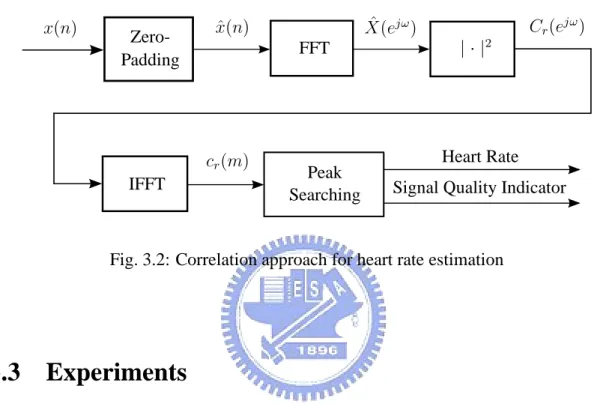
(26) 3.2 Correlation Technique for Heart Rate Estimation The heart rate is traditionally estimated as the average of the reciprocal of the R-R interval within a specific time window or as the number of heartbeats per unit time in ECG analysis. The proposed approach in this section is based on the idea of characterizing ECG signals as periodic signals with the period of R-R peaks for the fundamental frequency approximately. This is a classic problem of frequency estimation and has been studied for a long time [13]. The correlation method can be used to evaluate the correlation value and search the position where the R-wave event occurs. The correlation value based on self-correlated concept for a shifted length m is defined as below cr (m) =. X. x(n)x(n + m). (3.9). n. It sums up the products of the original signal x(n) and its shifted version x(n + m). If the signal x(n) is perfectly periodic, the peak correlation value occurs when the shifted length m equals the multiple of the signal period. Nevertheless, it is unsuitable for realtime process that computing the correlation value using (3.9) directly because of heavy calculation. As a result, we make use of the property that the correlation operation can be regarded as the convolution in a sense, and then Fourier transform is applied to reduce the computation. It can be shown that Cr (ejω ) =. X. cr (m)e−jωm. m. =. XX. x(n)x(n + m)e−jωm. =. XX. x(−k)x(m − k)e−jωm. m. m. n. k. XX = ( x(−k)e−j(−ω)(−k) )x(m − k)e−jω(m−k) m. k. = X(ejω )X(e−jω ) = X(ejω )X ∗ (ejω ) if x(n) is real Before operating the FFT, it is necessary to provide zero padding in time domain when the original signal is time limited (nonzero only over some finite duration spanned 15.
(27) by the original samples). This procedure allows the computation of the linear convolution or linear correlation of two finite-length sequences using FFT [14]. More zero padding yields denser interpolation of the frequency samples, and ideal sampling rate conversion is thus achieved. In signal processing, zero padding in time domain corresponds to a higher interpolation density in frequency domain. We will obtain the correlation value cr (m) by ˆ jω )|2 . Note that X(e ˆ jω ) is the FFT of xˆ(n), where xˆ(n) is taking the inverse FFT of |X(e the zero-padding version of x(n). In other words, the computation of correlation can be realized via the FFT and inverse FFT (IFFT) operation. As discussed earlier, the peak correlation values occur in every shifted length equal to the multiple of signal period if the signal x(n) is almost periodic. Then we just find the first peak position of the correlation value except for the region m less than 60 by direct searching, and the average R-R interval will be obtained. The reason why excluding that section is that the correlation value has much larger value in the section under 60 than the remaining particularly when two sequences have not shifted yet. The set value of 60 limits the maximum heart rate to 200 heartbeats per minute under the condition of the sampling frequency of 200 Hz. In general, the heart rate is expressed as heartbeats per minute according to the following formula Heart Rate = 60 ×. Sampling Frequency R-R interval. (3.10). However, ECG signals may be indistinct due to wearable dry electrodes, especially in motion of the wearing person. The peak effect of the correlation value vanishes when the signal quality degrades. Consequently, we propose a signal quality indicator i(n) to show how reliable the estimated heart rate is. The indicator is defined as the ratio of the difference between the position of the second peak and that of the first peak over the position of the first peak. Also, the peak value is easily found by direct searching from the correlation value. That is i(n) =. position of 2nd peak(n) − position of 1st peak(n) position of 1st peak(n). (3.11). Note that the index n is used in the indicator because the proposed estimator will compute one indicator value for each sample. If the signal is far away from periodic, the estimated 16.
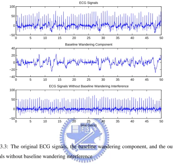
(28) heart rate through the above method should not be taken into account because the peak position is no longer the multiple of the signal period. When the indicator value i(n) is close to unity, the quality of ECG signals is better and the estimated heart rate will be more reliable. When i(n) is far away from unity, the estimated heart rate may be improper at this time. Fig. 3.2 illustrates the realization of this correlation method. x(n). ZeroPadding. Peak Searching. Cr (ejω ) | · |2. FFT. cr (m) IFFT. ˆ jω ) X(e. xˆ(n). Heart Rate Signal Quality Indicator. Fig. 3.2: Correlation approach for heart rate estimation. 3.3 Experiments Three experiments are presented to show the effectiveness of the proposed methods. We acquire the ECG data with 8-bit resolution and sampling rate of 200 samples per second via the smart shirt previously developed by Ming Young Biomedical Corporation. By experience, the vector length of the adaptive subspace approach is set to 40. Therefore, the output signals after the removal of baseline wandering interference will be delayed about 40/200 = 0.2 seconds with respect to original received signals. Consider the efficiency of the heart rate estimation, the chosen FFT or IFFT length of the proposed correlation approach is 2048. Hence, the first estimate occurs after about 10 seconds. Afterward, every new sample data will yield a new estimate and indicator. In the first experiment, we examine the performance of the adaptive subspace algorithm for the removal of baseline wander. Fig. 3.3 depicts three plots. The upper figure shows the original ECG data about 50 seconds measured via wearable sensors. The baseline wandering component estimated by the proposed approach is shown in the middle 17.
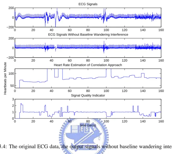
(29) ECG Signals 100 50 0 −50. 0. 5. 10. 15. 20. 25. 30. 35. 40. 45. 50. 35. 40. 45. 50. 40. 45. 50. Baseline Wandering Component 40 20 0 −20 −40. 0. 5. 10. 15. 20. 25. 30. ECG Signals Without Baseline Wandering Interference 100 50 0 −50. 0. 5. 10. 15. 20. 25 time (secs). 30. 35. Fig. 3.3: The original ECG signals, the baseline wandering component, and the output signals without baseline wandering interference. figure. The bottom figure exhibits the output signals after removing the baseline wander. This results demonstrate that the original ECG signals are contaminated with baseline wandering interference and the adaptive subspace technique gets rid of the baseline aberrations successfully. The second experiment demonstrates the performance of proposed heart-rate estimator. The ECG data are measured from the person who is wearing the smart shirt with wearable textile electrodes in intimate contact on the skin. The person is initially sitting still for about 30 seconds, then standing up and walking at a regular pace for about one minute, and finally jogging for near one minute. The received ECG data is shown in the first figure of Fig. 3.4. From this figure, we observe that the measured ECG signals involve in irregular aberrations in the intervals from 32 seconds to 46 seconds and from 96 seconds to 102 seconds because of the posture transitions of the wearing person. The 18.
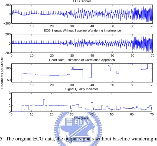
(30) ECG Signals 200 0 −200. 0. 20. 40 60 80 100 120 ECG Signals Without Baseline Wandering Interference. 0. 20. 40. 0. 20. 40. 60 80 100 Signal Quality Indicator. 0. 20. 40. 60. 140. 160. 140. 160. 120. 140. 160. 120. 140. 160. 200 0. Heartbeats per Minute. −200. 60 80 100 120 Heart Rate Estimation of Correlation Approach. 100. 50. 3 2 1 0. 80 time (secs). 100. Fig. 3.4: The original ECG data, the output signals without baseline wandering interference, the estimated heart rate in heartbeats per minute, and the signal quality indicator for the person with wearable sensors in tight contact on the skin. second figure exhibits the output signals after the removal of baseline wandering interference. The estimated heart rate in heartbeats per minute is shown in the third figure and the fourth figure depicts the signal quality indicator in the meanwhile. Note that the signal quality indicator is capable of discriminating the validness of the heart rate estimate by the relation with respect to unity as above mentioned. In this experiment, the heart rate, except in those intervals with degraded signal quality, is obtained correctly by virtue of the proposed heart-rate estimator and hence shows the viability of the method. Finally, we exhibit the heart rate estimation for ECG signals measured from the person with wearable sensors in loose contact on the skin instead of in tight contact. The original ECG data, the output signals without baseline wandering interference, the heart rate estimate, and the signal quality indicator are shown in Fig. 3.5. The posture of the person 19.
(31) ECG Signals 200 0 −200. 0. 10. 20 30 40 50 ECG Signals Without Baseline Wandering Interference. 60. 70. 0. 10. 20 30 40 50 Heart Rate Estimation of Correlation Approach. 60. 70. 0. 10. 20. 50. 60. 70. 0. 10. 20. 50. 60. 70. 200 0. Heartbeats per Minute. −200. 100. 50 30 40 Signal Quality Indicator. 3 2 1 0. 30. 40 time (secs). Fig. 3.5: The original ECG data, the output signals without baseline wandering interference, the estimated heart rate in heartbeats per minute, and the signal quality indicator for the person with wearable sensors in loose contact on the skin. also changes from sitting still initially through walking steadily until jogging. At first, the correct heart rate estimate is obtained in the period of sitting still. Afterward, erroneous results are acquired because the ECG signal quality degrades dramatically. Abrupt deflection is mainly caused by the loose contact of the sensors on the skin that results in the movement of wearable electrodes during the mobile period. The signal quality indicator distinguishes the accuracy of heart rate estimate appropriately. This experiment demonstrates that even if the ECG data with extremely poor signal quality may be obtained via wearable textile electrodes, the proposed estimator combined with the signal quality indicator can still extract useful information at most time.. 20.
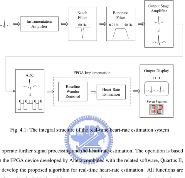
(32) Chapter 4 HARDWARE IMPLEMENTATION Numerous conditions should be taken into account to realize a real-time heart-rate estimation system through preceding approaches in practice. Above all, it is important to deal with the interference generated from the electrode-skin interface, the electric device, etc. Then, the power consumption should be low enough to monitor for long-term care. In the hardware implementation of the proposed algorithm, it is necessary to adopt an efficient design flow in order to reduce design time. We attempt to realize these methods on an field programmable gate array (FPGA) here for fast verification. The entire hardware architecture is illustrated later.. 4.1 Hardware Architecture Design The main purpose of this thesis is the design and implementation of a real-time heartrate estimation system for wearable sensors. The approaches in theory are elaborated previously. The integral hardware design includes ECG signal acquisition, preprocessing and module consolidation based on the real-time heart-rate estimator as well as results display. Fig. 4.1 depicts the entire hardware architecture. After receiving ECG signals from wearable textile electrodes, it is a primary step to filter the frequency distortion and power-line interference. Consequently, analog front-end circuits are provided. The circuits also adjust the amplitude of output voltage for the coordination of the analog-todigital converter. The ECG data through the A/D converter are transmitted to an FPGA 21.
(33) Notch Filter. ADC. . 60 Hz. 0.2 Hz. Output Stage Amplifier. 50 Hz. . FPGA Implementation. Output Display LCD. Baseline Wander Removal. . Instrumentation Amplifier. Bandpass Filter. 01011010. Heart-Rate Estimation Seven Segment. Fig. 4.1: The integral structure of the real-time heart-rate estimation system. to operate further signal processing and the heart rate estimation. The operation is based on the FPGA device developed by Altera combined with the related software, Quartus II, to develop the proposed algorithm for real-time heart-rate estimation. All functions are performed as individual modules so as to expand the system more easily in the future. Finally, we integrate all designed modules, which involve in the A/D converter control, baseline wander removal, heart rate estimation and output display control modules, with an FPGA and demonstrate results through an LCD and seven-segment displays for the exhibition of the originally measured ECG signals, the output signals after the removal of baseline wander, the estimated heart rate and the signal quality indicator.. 4.2 Analog Circuit Design The amplitude of original ECG signals is so weak (about 1mV) that it is necessary to amplify the signals to appropriate voltage level for observation. One of aims of the analog front-end circuits is to enlarge received ECG signals from the body, at least 0.5V prop22.
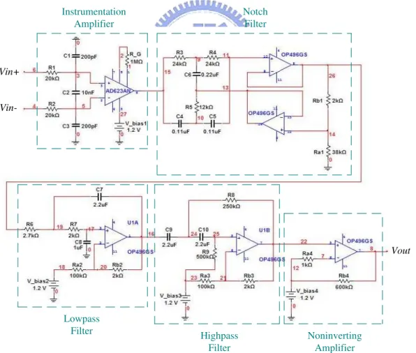
(34) erly. For this reason, the magnification of the designed analog circuit is set to 600, and the output voltage level will achieve 0.6V approximately under the consideration of the input voltage of the A/D converter ranging from 0V to 2.5V and the measured ECG signals which may have a baseline drift. However, unexpected disturbance and power-line interference may be amplified simultaneously as the analog circuits amplify weak ECG signals. The design of the analog front-end circuits should be taken into account for filtering out the power-line interference of 60 Hz, the adequate frequency band for signal processing (about from 0.5 to 50 Hz for the purpose of ECG monitoring), the suitable magnification, and the protection for users. A basic analog circuit consists of an instrumentation amplifier, a notch filter, a lowpass filter, a highpass filter and a noninverting amplifier. It is shown in Fig. 4.2. It is important that the whole circuits are manipulated in 3.3V single supply. Each part is introduced in detail respectively in this chapter. Instrumentation Amplifier. Notch Filter. Vin+. Vin-. Vout. Lowpass Filter. Highpass Filter. Noninverting Amplifier. Fig. 4.2: Basic analog circuits for signal preprocessing. 23.
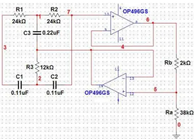
(35) 4.2.1 Pre-Amplifier The pre-amplifier should have a high input impedance and a high common-mode rejection ratio (CMRR) in general. An instrumentation amplifier is usually applied in the system and suitable as an ECG preamplifier. A typical instrumentation amplifier is the differential amplifier and contains several operational amplifiers. We accept AD623 that has the properties of low noise, low input bias current, and particularly the alternative mode of operation in 3.3V single supply. The value of RG was chosen to 1MΩ to avoid output saturation and the gain of this stage is approximate 1.. 4.2.2 Notch Filter Circuit Because the amplitude of original ECG signals is weak (about 1mV), the signals are easy to be affected by 60 Hz power-line interference or noise from surroundings. To eliminate unwanted mains hum at 60 Hz, the notch filter is generally used. In this study, we adopt a twin T circuit as a notch filter which provides a large degree of rejection at a specific frequency with the consideration of its simple circuit. The circuit of a twin T notch filter is shown in Fig. 4.3. We simulate this circuit by MultiSim program to confirm the characteristic, and the result is performed in Fig. 4.4.. Fig. 4.3: Notch filter. 24.
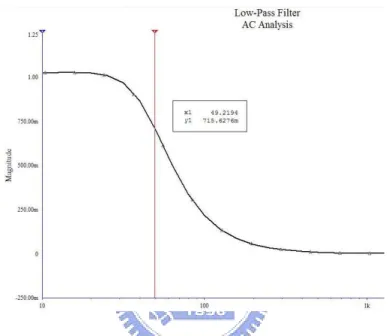
(36) Fig. 4.4: Frequency response of the designed notch filter. 4.2.3 Lowpass Filter Circuit To get rid of high-frequency noise, we can cascade several RC filters. Unfortunately, the impedance of one RC section affects the next stage and leads to that the pass and stop bands will not be sharp enough. Therefore, we choose the Sallen-Key active filter to reduce the interference without degrading desired signals [15].. Fig. 4.5: Second order Sallen-Key lowpass filter. A generic second order Sallen-Key lowpass filter as shown in Fig. 4.5 uses four resistors, two capacitors and an unity gain operation amplifier. Note that Ra and Rb are applied 25.
(37) for setting the offset voltage because the operational amplifier, OP496GS, also uses 3.3V single supply. The cutoff frequency fc is obtained by the following equation fc =. 1 2π R1 R2 C1 C2 √. (4.1). Finally, Fig. 4.6 exhibits the simulation result of the designed lowpass filter in frequency domain. The cross marks the cutoff frequency at about 50 Hz.. Fig. 4.6: Frequency response of the designed lowpass filter. 4.2.4 Highpass Filter Circuit In the same way, a second order Sallen-Key highpass filter is adopted to remove lowfrequency interference. Fig. 4.7 is the circuit of the highpass filter that we designed. The cutoff frequency fc is computed also by (4.1) and was set to 0.2 Hz. The result of simulation is shown in Fig. 4.8.. 4.2.5 Output Stage Amplifier The output voltage is not high enough when through an pre-amplifier and several filters, and it may result in extremely terrible quantization errors due to the constrain of analogto-digital conversion. Consequently, a noninverting amplifier with a large gain, as shown 26.
(38) Fig. 4.7: Second order Sallen-Key highpass filter. Fig. 4.8: Frequency response of the designed highpass filter. in Fig. 4.9, is applied in the output stage. In addition, the output with a offset voltage is expected because of the demand of the A/D converter which we selected. The output voltage is computed as below Vout = (1 +. Rb )Vin + Vbias Ra. (4.2). The Ra and Rb were chosen to 1 kΩ and 600 kΩ respectively and the gain of the output amplifier will achieve 600 approximately. The bias voltage of 1.2V is provided by the 27.
(39) Fig. 4.9: Output stage amplifier. internal voltage regulator of the A/D converter... 4.3 Analog-to-Digital Converter After receiving from wearable sensors and preprocessing, ECG signals without redundant interference should be converted from analog to digital first in order to facilitate the signal processing on an FPGA for estimating the heart rate in real time. We adopt LTC1282, the analog-to-digital converter which Linear Technology produced. The LTC1282 is a 140ksps, sampling 12-bit A/D converter with 6µs maximum conversion time that draws only 12mW from a single 3V or dual ±3V supply. We use the unipolar conversion mode which converts 0V to 2.5V unipolar inputs from a 3V single supply because of the condition in our system. Fig. 4.10 illustrates the typical application with a 3V single supply and detail explanations of control lines will be discussed in the next chapter. Finally, pin functions divided into inputs and outputs of LTC1282 are exhibited as follows. • Inputs: – Ain : Analog input. 0V to 2.5V (Unipolar), ±1.25V (Bipolar). – HSBN : High byte enable input. This pin is used to multiplex the internal 12-bit conversion result into the lower bit outputs.. 28.
(40) 1.20V Vref OUTPUT. ANALOG INPUT (0V to 2.5V). 10P F. 0.1P F. BUSY. 10P F. 8- OR 12- BIT PARALLEL BUS. CS. ° ° ° ° ° ° ° ° ° ® ° ° ° ° ° ° ° ° °¯. RD. 0.1P F. ½ ° ¾ P P CONTROL ° LINES ¿. Fig. 4.10: Analog-to-digital converter, LTC1282. – CS : The chip select input must be low for the ADC to recognize RD and HSBN inputs. – RD : Read input. The active low signal starts a conversion when CS and HSBN are low. • Outputs: – Vref : +1.2V reference output. – BUSY : The BUSY output shows the converter status. It is low when a conversion is in progress. – D11-D4 : Three-State data outputs. D11 is the most significant bit. – D3/11-D0/8 : Three-state data outputs.. 29.
(41) Chapter 5 FPGA IMPLEMENTATION AND EXPERIMENTAL RESULTS Digital system design in the past was built at the board level using standard components such as TTLs and CMOSs, or at the gate level in application-specific integrated circuits (ASIC). It takes quite not only a lot of time for verification but also expensive cost in redesigning. In addition, problems due to signal propagation delay may be arisen, and it is time-consuming to solve them. With the advent of programmable logic, digital circuit design becomes more simple and functions are confirmed more easily. In this thesis, an FPGA is applied on verification for the proposed real-time heart-rate estimator. The advantages include a shorter time to market, ability to re-program for fixing bugs, and lower non-recurring engineering costs. Algorithms can be developed on regular FPGAs and then migrated into a fixed version that resembles an ASIC. At the same time, FPGAs offer another way from a traditional gate-level design to gate-level or register-transferlevel (RTL) design of a hardware description language (HDL). The HDL is easier to work with when handling large structures because it allows the designer to express both the behavioral and structural aspects of each stage in the design. The behavioral features similar to a conventional high-level language are those structural constructs that allow description of the instantiation and interconnection of modules. The block diagram of hardware implementation procedure is shown in Fig. 5.1. We accept the FPGA which Altera developed for the hardware implementation of 30.
(42) Procedure ASIC Algorithm. Verilog (VHDL) FPGA Verification. Fig. 5.1: Hardware implementation procedure. the heart-rate estimator of the proposed system. The way of consolidation of designed modules was adopted to accomplish the integral system. The virtue of this manner is that every component among the system whatever users designed by themselves or vendors provided can be utilized flexibly and modified if you need. The system becomes easier to be expanded in the future. In this chapter, we exhibit all the modules which we designed and a full scheme of the system. Finally, the measured performance of the proposed real-time heart-rate estimation system for wearable sensors is demonstrated in practice.. 5.1 Introduction to FPGA Systems A field-programmable gate array (FPGA) is a semiconductor device containing programmable logic components called “logic element”. Logic elements can be programmed to perform the function of basic logic gates such as AND and XOR, or more complex combinational functions such as decoders and mathematical functions. To raise the speed of verification and system efficiency, we accept the Cyclone II FPGA which Altera developed for the hardware implementation, and it offers the following features. • EP2C35F672 Cyclone II FPGA Chip • High-density architecture with 33216 LEs (Logic Elements) • M4K embedded memory blocks • Up to 35 18 × 18-bit multipliers are each configurable as two independent 9 × 9-bit multipliers 31.
(43) • A 2.0 inch low temperature poly-silicon (LTPS) LCD • Up to four PLLs per device provide clock multiplication and division, phase shifting, programmable duty cycle, and external clock outputs, allowing system-level clock management and skew control • Supports two configuration modes: active serial and JTAG-based configuration • Supports Intellectual Property (IP) including Altera megafunction and Altera MegaCore function In the previous chapter, we presented an adaptive baseline wander removal algorithm and a correlation technique for heart rate estimation. The former is based on the subspace approach and the latter is realized via the FFT and inverse FFT (IFFT) operation. After completing the development of our algorithms in Matlab environment, we need the Verilog HDL to describe our hardware structure. The resulting Verilog codes can be compiled and synthesized in Quartus II, which is developed by Altera also. Through JTAG-based configuration, we download the results to the FPGA device for verification.. 5.2 Modular Design of the Real-Time Heart-Rate Estimator In the hardware implementation of the proposed algorithm, an efficient design flow to reduce design time is necessary. First we separate the entire real-time heart-rate estimator of the proposed system roughly into several basic modules, those are the A/D converter control, baseline wander removal, heart rate estimation and output display control modules. All of them are designed independently and constructed in the form of intellectual property (IP) that can be reused easily in other applications. Fig. 5.2 depicts the modular design of the proposed estimator. We have to add an additional input port and output port, “input available” and “output available”, in each module for synchronization. Explanations of the modules are elaborated as below.. 32.
(44) RAM. Dout 12. I/O. ADC Control Module. BUSY. Baseline Wander Removal Module. 12. BWR_out_available. MUX 4x1 BWR_out. 8. LCD Control Module. Absolution Module MUX 4x1 12. abs_out_available. RAM. LCD_DATA. abs_out. I/O. LCD_in_available. RAM. Heart Rate Estimation Module. 9 HRE_out_available. 9. SQI_out. HRE_out. Seven-Segment Control Module. I/O. Fig. 5.2: Modular design of the real-time heart-rate estimator. 5.2.1 A/D Converter Control Module The analog-to-digital converter which we adopted, LTC1282 of Linear Technology, has an internal clock, and hence it has no need for synchronization between the external clock and the control lines. The internal clock is trimmed to achieve a typical conversion time of 5.5µs. Conversion start and data read operation are controlled by three inputs: HSBN, CS and RD. There are two modes of operation according to different inputs. We set HSBN to low and enable slow memory mode with parallel read. Regulating CS and RD low at the sampling frequency 200 Hz brings a read operation. Conversion status is indicated by the BUSY output, and it is low while the conversion is in progress. BUSY returns high at the end of conversion and the result is placed on data outputs D11,...,D0 in parallel. Fig. 5.3 depicts the timing diagram of the A/D converter, LTC1282. By way of setting this LTC1282 control module as shown in Fig. 5.4, we can adjust the sampling frequency of the A/D converter. The function and bit usage of each pin are listed in Table 5.1. 33.
(45) CS. RD. tconv BUSY. DATA. OLD DATA. NEW DATA. HOLD TRACK. Fig. 5.3: Timing and control diagram of LTC1282. Fig. 5.4: A/D converter control module. 5.2.2 Baseline Wander Removal Module The baseline wander removal module as shown in Fig. 5.5 is to realize the adaptive subspace algorithm summarized as follows. p(n) = αp(n − 1) + (1 − α)x(n)T q(n − 1)x(n). (5.1). q(n) =. p(n) k p(n) k. (5.2). b(n) = xT (n)q(n)q(n). (5.3). y(n) = x(n) − b(n). (5.4) 34.
(46) Table 5.1: Signal Definition of the A/D Converter Control Module pin. I/O. size (bits). function. SYS clk. INPUT. 1. system clock. BUSY n. INPUT. 1. BUSY. D11-D0. INPUT. 1. each bit of digitalized data. CS n. OUTPUT. 1. CS. RD n. OUTPUT. 1. RD. Dout. OUTPUT. 12. digitalized data. Fig. 5.5: Baseline wander removal module. The function and bit usage of each pin are listed in Table 5.2. Table 5.2: Signal Definition of the Baseline Wander Removal Module pin. I/O. size (bits). function. CLK. INPUT. 1. module clock. RESET n. INPUT. 1. reset signal. IN. INPUT. 12. input signal. IN VALID. INPUT. 1. input available signal. OUT. OUTPUT. 12. output signal. OUT VALID. OUTPUT. 1. output available signal. 35.
(47) The computation involved in an adaptive baseline wander removal algorithm performs sequentially and hence needs a control unit to decide a process of the square root operation, the inner product, the addition of vectors, etc. The control circuit is implemented as a finite state machine (FSM). This is an often used method in constructing control units. There are two different kinds of FSM, Moore and Mealy [16]. The output of a Moore machine is only dependent on the current state and delayed one clock cycle. The output of Mealy machine is dependent on both the current state and the input. Decisions in all modules of our system are made using the Mealy machine. Four states were introduced to control the processing stage of the baseline wander removal algorithm. The first state, idle, is a reset state where the processor does nothing and is waiting for a starting signal. When the signal “input available” turns to “0”, the processor begins working, and the state changes from idle to inputBWR. The signal “input available” is connected to BUSY from the analog-to-digital converter which is low when the conversion is in progress. Next, three state, the inputBWR, computeBWR and outputBWR, perform sequentially. There are two approaches to transfer between each of them. One is to generate the state signal by each stage. The other is to use a stage generator according to the period of each state. The most difference between two approaches is that constant periods are necessary in the latter approach, while not in the former. Since we cannot predict the exact time that the conversion finished, the first approach is chosen in the design of the baseline wander removal module. Fig. 5.6 illustrates the state transfer flow chart of the baseline wander removal module. Moreover, the working frequency of the baseline wander removal module and the heart rate estimation module is set to 6 MHz. input_available=0. inputBWR. idle. output_available=1. input_available=1. computeBWR. outputBWR. done=1. Fig. 5.6: State transfer flow chart of the baseline wander removal module. 36.
(48) By experience, the length of the vectors involved in the adaptive subspace approach, x(n), p(n) and q(n), is set to 40. Thus three on-chip RAMs with 40 words are applied to save the data. The bit usages of these three vectors x(n), p(n) and q(n) are 12 bits, 26 bits and 10 bits respectively. During the inputBWR part, it is necessary to wait for the rising edge of the signal BUSY so as to ensure that the conversion of the ECG data has finished. Then the digitalized ECG signal will be received and saved in the RAM. Every received input datum is stored in the leading component of x(n), and the components of x(n) should be shifted backward in theory at every time the datum enters. However, the write/read properties of RAMs prevent us from doing this. We then use an one-shot circuit to produce a “write enable” signal and a counter to generate a recurring write address combined with an indicator to mark the latest component of the vector. In the computeBWR phase, according to the equation (5.1) the first step is computing the inner product of two vectors, x(n), q(n − 1) where n − 1 denotes the values at the preceding moment. Since a sampling rate is set to 200 and each sample is represented by 12 bits, we should put more emphasis on the hardware resource utilization rather than the speed when designing the architecture of the system. Base on this idea, only one multiplier and one accumulator is required to complete the inner product operation. Above all, a dynamic bit allocation of the data path within each module is important in the hardware implementation and will significantly affect the integral performance. We scale up the values of q(n) by 210 and normalize the result of inner product to 1/1024 of the original result, so that it can be easily realized by shifting right 10 bits and avoid mistaking the final result because each component of q(n) is normally less than unity. Afterward, the multiplication for 1 − α, x(n) and the inner product of x(n) and q(n − 1) are continuously done in pairwise. After copying with the multiplied parts of (5.1), an adder is required. On the other hand, 1 − α and α need to be scaled up by 212 and the final result is then shifted right. Note that the word length of the addend and summand should be long enough for fear of the possible overflow situation. Next step is to realize (5.2) using one divider. Prior to division, the norm of p(n) should be computed first. The preceding multiplier and accumulator are also used in cal37.
(49) culating the square value, kp(n)k2 . Of course, it still requires a module to compute its square root value. However, it is a burden for the bit usage of the square value. Simultaneously, the denominator’s bit numbers of the divider are too many and will be a load in the speed of computation. Because each component of q(n) is less than unity, we scale up the values by 210 on the numerator of the divider, and it leads to the increase of the numerator’s bit numbers as well. Consider the performance and the hardware utilization, it is imperative to reduce the bit usage. We can shift right 10 bits in the denominator, that is the norm, to achieve the purpose of bit reduction. In other words, multiplying by 210 in the numerator is equal to multiplying by 2−10 in the denominator, and the bit necessity of the square value will obviously decrease a lot. Afterward, along the equation (5.3), the preceding multiplier and accumulator are also applied to compute the inner product of x(n) and q(n). After calculating, we make the latest component of q(n) be multiplied by the inner product value and yield to a baseline wander component. Finally, we obtain the output signal by subtracting the baseline wander component from the latest component of the input signal vector, x(n), and the signal “done” will be set in order to represent the end of the computation. The state is transferred from computeBWR to outputBWR. As the output signal is passed to the next module, we send the synchronization signal “output available” in the meanwhile.. 5.2.3 Heart Rate Estimation Module Before we construct the heart rate estimation module, we have to build two necessary basic modules, the FFT and IFFT modules. Since there is the same architecture on the whole in the FFT and IFFT processor, the FFT module is mainly introduced here, and the IFFT will be formed similarly. In this thesis, we adopt the decimation-in-frequency FFT algorithm [14] with the input sequence in normal order and the output in bit-reversed order. In the FFT processor, four states were presented to control the stage and the state transfer flow chart is shown in Fig. 5.7. The first state, idle, is a reset state where the FFT processor does nothing. When the signal “input available” is true, the FFT processor starts working, and the state changes from idle to inputFFT. Three state, the inputFFT, 38.
(50) inputFFT. idle. computeFFT. outputFFT. Fig. 5.7: State transfer flow chart of the FFT module. computeFFT and outputFFT, perform sequentially. We choose the approach that three parts generate state signals by themselves. The state, inputFFT, lasts N clock cycles where N denotes the length of the FFT operation, that is, there are N input data received in the processor. N is 1024 in the design of our real-time heart-rate estimator with the consideration to achieve balance between the performance and the hardware utilization. The period of the computeFFT part is 1024 × 10 = 10240 clock cycles because there are log2 1024 = 10 stages in the computation of the FFT algorithm and each stage requires N clock units. The outputFFT phase also lasts N clock cycles to deliver N output data. Every state generates their own state signals, input s, compute s and output s respectively, after the work of each state. The primary work of the inputFFT is to produce the address and transfer the input data with 32-bit words (the first 16 bits are the real part, whereas the remaining are the imaginary part) to on-chip RAMs. Addresses are the indices of the input data. During the computeFFT part, the basic computation performs with a butterfly computation. Fig. 5.8 demonstrates a butterfly computation in hardware implementation where the “opA” and “opB” are two operands, while the “TF” denotes the twiddle factor. All arithmetic operations are carried out as signed operations. Note that the operator of dividing by 2 is shown only for classification purpose and it is realized using a shift operation. It is necessary to divide the results of butterfly computations by two to avoid saturation. With the design consideration, the most significant bits (MSB) can be maintained after a series of computation, such as addition and multiplication, to avoid the possible overflow. 39.
(51) opA. resultA. TF. opB. resultB. -1. opA[real]. opA[img]. opB[real]. TF[real]. /2. /2. resultA[real]. resultA[img]. /2. opB[img]. TF[img]. resultB[real]. /2. TF[real]. resultB[img]. Fig. 5.8: Butterfly computation. situation. After the computation of 10 stages, the outputs are reduced to 1/1024 of the outputs of the regular FFT. Furthermore, how to generate twiddle factors is another import problem. It is impossible to use a cosine processor in the FFT processor because it would consume both hardware and time resources. We attempt to use a ROM by a simple look-up-table process. The ROM with 512 words is pre-stored in the computed twiddle factors that are calculated by Matlab program. Twiddle factors require to be scaled up by 211 , and they are 12 bits with one signed bit since they are less than or equal to unity. Maybe the size of the ROM can be smaller using some properties of twiddle factors, but we do not discuss here. We set the word length of the twiddle factor to 24 bits where 12 bits for the real part and 12 bits for the imaginary part. There are two butterfly computations used to accomplish the FFT processor. Combined with the memory assignment of two RAMs which will be described later, the efficiency to compute the FFT algorithm can be improved in the hardware implementation. 40.
(52) The main function of the outputFFT is to generate the address and send the output data from RAMs in digit-reversed order. Address are the digit reversal of the indices for the output data. There are two RAMs used in the architecture of the FFT processor. The real and imaginary parts of a complex value are stored as a single word with 32 bits. It is a important step to design the addressing criterion for the memory and resource assignment in the inputFFT, computeFFT and outputFFT parts. Because the computeFFT performs in-place computation, its memory assignment is the basis of the addressing rules of the inputFFT and outputFFT phases. There is a feasible memory assignment [17], which is always storing two data for the FFT algorithm in different memories. This method provides a mapping from data index to RAM address. A variable with index i is assigned to RAMP (i) using an XOR pattern where P (i) = i0 ⊕ i1 ⊕ · · · ⊕ iL−1. (5.5). and L is the length of binary representation of i. In other words, it is determined by P (i) to decide which RAM the datum will be stored in. Memory assignment of various FFTs. 10. 11. 12. 13. 14. 15 RAM0. RAM0. 9. RAM1. RAM1. 8. RAM1. RAM0. 7. RAM0. RAM1. 6. RAM1. 5. RAM0. 4. RAM0. 3. RAM1. 2. RAM1. 1. RAM0. 0. RAM1. Data index Data x(i). RAM0. are shown in Fig. 5.9.. 2-point FFT 4-point FFT 8-point FFT 16-point FFT. Fig. 5.9: Memory assignment for various FFTs [17]. In the computeFFT part, we use the addressing algorithm described in the chapter 9 of the reference [17]. The index generation for data is described by the following indices. 41.
(53) for the variables: Ns =. N. (5.6). 2stage. k1 = 4Ns ⌊. m ⌋ + m mod(Ns ) Ns. kˆ1 = k1 + Ns k 1 + Ns 2 k2 = k + 2N 1 s. (5.7) (5.8). Stage = 1. (5.9). Stage ≥ 2. kˆ2 = k2 + Ns. (5.10). p = k1 2stage−1 mod(. N ) 2. (5.11). where the variable m is the index and 0 ≤ m ≤ N/4 − 1 = 255. When P (m) = 0, k1 from RAM0; address k1 mod(N/2) to Butterfly0 kˆ1 from RAM1; address kˆ1 mod(N/2) to Butterfly0 k2 from RAM1; address k2 mod(N/2) to Butterfly1 kˆ2 from RAM0; address kˆ2 mod(N/2) to Butterfly1 When P (m) = 1, k1 from RAM1; address k1 mod(N/2) to Butterfly1 kˆ1 from RAM0; address kˆ1 mod(N/2) to Butterfly1 k2 from RAM0; address k2 mod(N/2) to Butterfly0 kˆ2 from RAM1; address kˆ2 mod(N/2) to Butterfly0 In this algorithm, the m does not necessarily be increased in binary order. The index m can be incremented in Gray code order to avoid computing the function P (m) for every m because Gray code has the property that only one bit changes once. Hence the function P (m) will switch every time. According to the algorithm, k1 or k2 is from one memory, while kˆ1 or kˆ2 is from the other. Then, there is no switch between two RAMs and butterflies in hardware. For instance, P (kˆ1 ) is always the inverse of P (k1) since kˆ1 is computed by setting one bit in k1 . The operation flow for two RAMs and two butterfly computations is shown in Fig. 5.10. In the inputFFT and outputFFT parts, we transfer N complex data sequentially in the 42.
數據
![Fig. 2.1: Representative electrical activity from various regions of the heart [9]](https://thumb-ap.123doks.com/thumbv2/9libinfo/8629924.192274/17.892.190.711.305.714/fig-representative-electrical-activity-various-regions-heart.webp)
+7

相關文件
了⼀一個方案,用以尋找滿足 Calabi 方程的空 間,這些空間現在通稱為 Calabi-Yau 空間。.
We do it by reducing the first order system to a vectorial Schr¨ odinger type equation containing conductivity coefficient in matrix potential coefficient as in [3], [13] and use
• ‘ content teachers need to support support the learning of those parts of language knowledge that students are missing and that may be preventing them mastering the
• helps teachers collect learning evidence to provide timely feedback & refine teaching strategies.. AaL • engages students in reflecting on & monitoring their progress
Robinson Crusoe is an Englishman from the 1) t_______ of York in the seventeenth century, the youngest son of a merchant of German origin. This trip is financially successful,
fostering independent application of reading strategies Strategy 7: Provide opportunities for students to track, reflect on, and share their learning progress (destination). •
Strategy 3: Offer descriptive feedback during the learning process (enabling strategy). Where the
• A put gives its holder the right to sell a number of the underlying asset for the strike price.. • An embedded option has to be traded along with the
