國
立
交
通
大
學
電子工程學系 電子研究所
博 士 論 文
應用於地面及手持數位電視廣播與室內無線接
收機之同步設計
Synchronization Design for DVB-T/H and
Indoor Wireless Receiver
研 究 生:魏庭楨
指導教授:周世傑教授
應用於地面及手持數位電視廣播與室內無線接
收機之同步設計
Synchronization Design for DVB-T/H and
Indoor Wireless Receiver
研 究 生:魏庭楨 Student:Ting Chen Wei
指導教授:周世傑 教授 Advisor:Prof. Shyh-Jye Jou
國 立 交 通 大 學
電子工程學系 電子研究所
博 士 論 文
A Dissertation
Submitted to Department of Electronics Engineering and Institute of Electronics
College of Electrical and Computer Engineering National Chiao Tung University
in partial Fulfillment of the Requirements for the Degree of
Doctor of Philosophy in
Electronics Engineering May 2011
Hsinchu, Taiwan, Republic of China
應用於地面
及手持
數位電視廣播與室內無線
接收機之同步設計
研究生:魏庭楨 指導教授:周世傑 教授 國立交通大學 電子工程學系 電子研究所博士班摘要
在此篇論文中,提出應用於手持及地面數位電視廣播與室內無線 60GHz 規格 之同步設計。本論文探索基頻數位信號處理演算法和架構,以達成所要求之系統 規格。此外,整合與實現低功率及有效率的資料路徑,以驗證所提出之基頻設計。 為了完成同步設計,本論文採用並修改數個廣泛使用的資料路徑,像是移動總合 架構、單埠記憶體式延遲線、差值編碼、迴路濾波器、複數乘法器、座標旋轉數 位運算演算法與直流錯誤移除方法來有效率地實現同步之硬體。 提出之手持及地面數位電視廣播基頻接收機包含,模式、符元及保護區間偵 測、載波頻率與取樣時脈同步、快速兩階段之散佈領航碼同步與通道估測。保護 區間偵測採用無除法之相關方法。載波同步與取樣時脈同步使用記憶體分享架 構。快速兩階段之散佈領航碼同步方法加速領航碼位置之偵測。為了增加記憶體 使用率,通道估測重新利用符元偵測之記憶體。此外,差值編碼減少記錄領航碼 位置的儲存器之使用量。相位預測方法減少相位累加器之操作次數。系統模擬結 果顯示此接收機可達位元錯誤率之要求。最後,此接收機之晶片使用 0.18µm 互 補式金氧半導體技術製造和驗證,其核心面積為 12.96 mm2 。對於應用於 60GHz 之室內無線規格,此篇論文提出用於正交分頻多工與單載 波接收機之雙模架構。標頭與符元偵測、載波頻率與取樣時脈同步與部分的通道 估測共用於正交分頻多工模式與單載波模式,以減少硬體複雜度。此外,提出一 個應用於取樣頻率誤差補償器之平行化架構。此平行取樣頻率誤差補償器解決內 插器之不規則存取並加速處理速度。合成結果顯示,在使用 90nm 互補式金氧半 導體技術下,此架構可操作於 400 MHz 且在八倍平行化下可達到 3.2Gs/s,而其 等效邏輯閘數約為 204K。
Synchronization Design for DVB-T/H and
Indoor Wireless Receiver
Student:Ting Chen Wei Advisor:Prof. Shyh-Jye Jou Department of Electronics Engineering
Institute of Electronics National Chiao Tung University
Abstract
In this thesis, synchronization designs for DVB-T/H and indoor wireless 60GHz standards are present. Baseband digital signal processing algorithms and architectures are explored to achieve the required system specifications. Moreover, low power and area efficient data-paths are integrated and implemented to verify the proposed baseband designs. To accomplish synchronization designs, several widely used data-paths, such as the moving sum architecture, the single port based delay line, the differential encoding scheme, the loop filter, the complex multiplier, CORDIC algorithm and the removing DC error scheme are adopted and modified to implement the hardware of synchronizations efficiently.
The proposed DVB-T/H baseband receiver contains a mode/symbol/guard interval detection, a carrier frequency and sampling clock synchronization, a two-stages fast scattered pilot synchronization, and a channel estimation. The guard interval detection adopts a division free correlation method. The carrier synchronization and sampling clock synchronization uses a memory sharing
speed of the detection of pilot location. To increase memory utility, the channel estimation reuses the memory of the symbol detection. Besides, the differential encoding scheme reduces the storage requirement of recording pilot location. The phase predictive scheme reduces the operations of phase accumulators. The system simulation results show this receiver can achieve BER requirement. Finally, the chip of this receiver was fabricated and verified in a 0.18µm CMOS technology and its core size is 12.96 mm2.
For indoor wireless 60GHz standards, this thesis presents a dual mode architecture of the OFDM/single carrier mode receiver. The preamble/symbol detection, the carrier and sampling clock synchronization, and parts of channel estimation are shared in OFDM mode and SC mode to reduce hardware complexity. Besides, a parallel architecture for a sampling clock offset compensator is proposed. The parallel sampling clock offset compensator solves the irregular access form interpolators and increases the speed of processing. The synthesis result shows that it can operate at 400 MHz and achieve 3.2 Giga samples per second with a 8X parallelization with about 204 K equivalent gate counts by using 90nm CMOS process.
誌 謝
首先要感謝的是指導教授周世傑博士,教授提供良好的研究環境,並且適時 地給予建議和協助解決研究上的問題,使此篇論文能順利完成。然後要感謝口試 委員,陳紹基博士、吳安宇博士、劉志尉博士、許騰尹博士與薛木添博士,委員 們在口試時給予的建議與指教,讓這本論文更加的完善。此外要感謝在數位電視 廣播接收機計畫與室內無線接收機計畫中,參與教授們與同學們所提供的幫忙與 協助,並感謝緒祥同學所提拱的快速傅立葉轉換模組,讓晶片實作得以完成。接 下來要感謝的是實驗室的同學們,在做研究時互相的砥礪,並感謝瑋昌學弟與琪 耀學弟在研究上的幫助。最後,要感謝在背後支持我的家人們。Contents
Chapter 1 Introduction and Motivation ... 1
1.1 Motivation ... 1
1.2 Thesis Organization ... 3
Chapter 2 Overview of Channel Model and the Effects of Frequency Offset ... 4
2.1 Channel Model ... 4
2.2 Effects of Frequency Offset ... 6
2.2.1 Effects of Sampling Clock Offset ... 6
2.2.2 Effects of Carrier Frequency Offset ... 9
2.3 AWGN ... 12
2.4 Link Budget ... 14
2.5 Summary ... 18
Chapter 3 Data-path in a Baseband Receiver ... 19
3.1 Moving Sum Architecture ... 19
3.2 Delay Line ... 20 3.3 Differential Encoding [13] [26] [27] ... 21 3.4 Complex Multiplier ... 22 3.5 Loop Filter ... 23 3.6 CORDIC ... 26 3.7 Removing DC error... 28
3.8 Fast Fourier Transform ... 30
3.9 Summary ... 32
4.1 Introduction of DVB-TH ... 33
4.2 Baseband Receiver Architecture ... 35
4.3 GI Detection [10] [11] [12] ... 36
4.4 CFO and SCO synchronization ... 40
4.5 Scattered Pilots Synchronization [11] [13] [14] ... 48
4.6 Equalizer [10] [11] ... 51
4.7 Hardware Implementation ... 54
4.8 Summary ... 60
Chapter 5 SC-FDE/OFDM Receiver for 60 GHz ... 62
5.1 Introduction of standards for 60GHz ... 62
5.2 Consideration of Dual Mode Architecture Design... 65
5.3 CFO/SCO Synchronization ... 69
5.4 Behavior Simulation of OFDM (HSI) mode ... 70
5.5 Simulation of SCO Compensation ... 72
5.6 Proposed Parallelized SCO Compensator ... 77
5.6.1 Time Interpolation ... 77
5.6.2 Parallel Elastic Buffer ... 79
5.6.3 Parallel NCO ... 81
5.6.4 Proposed Parallelized Time Interpolation Architecture ... 82
5.6.5 Parallelized Frequency Rotation ... 83
5.6.6 Implementation Results of SCO Compensation ... 84
5.7 Summary ... 87
Chapter 6 Conclusion ... 89
Chapter 7 Future Work ... 91
List of Tables
TABLE 1-1 Characteristic of DVB-T/H and 60GHz standards ... 3
TABLE 3-1 Comparisons of hardware complexity ... 20
TABLE 3-2 Comparisons of different implementations of delay line (8K × 12) [10] [11] [12] ... 21
TABLE 3-3 Comparisons of different implementations of memory (64 ×64) ... 21
TABLE 3-4 Comparisons of different complex multiplier ... 23
TABLE 3-5 Comparisons of implementations of CORDIC ... 28
TABLE 3-6 Synthesis comparisons of an interpolation with and without the removing DC ... 30
TABLE 3-7 General comparison of FFT architectures ... 31
TABLE 4-1 Specification of DVB-T/H [1] [2] ... 34
TABLE 4-2 Comparison of memory usage of ICFO, RCO and SCO ... 42
TABLE 4-3 Hardware complexity of PB and CB Algorithm ... 50
TABLE 4-4 Required SNR for different Modes, channels and modulations ... 57
TABLE 4-5 Synthesis results ... 58
TABLE 4-6 Comparison between previous reported DVB-T/H [51] receiver with this work ... 60
TABLE 5-1 Comparison of 802.15.3c [3] and 802.11ad [4] ... 63
TABLE 5-2 Comparison of OFDM and SC... 65
TABLE 5-4 Comparison of CFO Estimations ... 67 TABLE 5-5 Synthesis results of an Cubic-Spline interpolator of different process... 78 TABLE 5-6 Synthesis results ... 87
List of Figures
Fig. 2-1 DVB-T/H channel models provided by [1] [2] ... 5
Fig. 2-2 802.15.3c channel models provided by [18] and only print the first 100 samples ... 6
Fig. 2-3 Eye diagram accumulated 50000 samples (12X oversample, raised cosine pulse shaping, and no AWGN) in a SC system (a) without SCO effect (b) with 50ppm SCO ... 7
Fig. 2-4 Constellation rotation and dispersion (QPSK and no AWGN) caused by SCO in a OFDM system (a) with 50ppm SCO (b) with 500ppm SCO ... 8
Fig. 2-5 Two methods of adding SCO (a) resample based method and (b) fractional delay filter based method ... 9
Fig. 2-6 QPSK constellation rotation caused by CFO (a) a SC data block in time domain (b) an OFDM symbol in the frequency domain ... 11
Fig. 2-7 Illustration of SNR and Es/N0 in over-sampling ratio equal to 4 (U = 4) ... 13
Fig. 2-8 Power spectrum density after passing a low-pass filter or a decimation filter ... 14
Fig. 2-9 Comparison of SNR and Eb/N0 in an oversampling system ... 14
Fig. 2-10 Link budget of a receiver ... 15
Fig. 2-11 LDPC performance for MCS1, 2, 3 [23] ... 17
Fig. 3-1 Moving sum architecture [25] ... 20
Fig. 3-3 Differential encoding of continual pilot positions of DVB-T/H [13] [26] [27] ... 22 Fig. 3-4 Architectures of complex multiplier (a) 4 „×‟ and 2 „+‟ (b) 3 „×‟ and 5 „+‟ [28] [29] ... 23 Fig. 3-5 Architecture of a loop filter [25] [30] on the CFO loop ... 24 Fig. 3-6 Tracking curves of different filter coefficients for CFO loop in a 802.15.3c baseband receiver ... 24 Fig. 3-7 Different combinations of Kc and Kd (a) Kd = 1, (b) Kd = 4, (c) Kd =
8, (d) Kd = 16, (e) Kd = 32, (f) Kd =64, ... 25
Fig. 3-8 Implementation of CORDIC (a) folding architecture (b) unfolding architecture [34] [35] ... 27 Fig. 3-9 Hardware implementation of Multiply-Add (a) original (b) removing DC error version ... 29 Fig. 3-10 Simulation of removing DC error (a) original (b) removing DC error version ... 29 Fig. 3-11 Output order of FFT (a) normal order (b) reversed order ... 30 Fig. 3-12 2K/4K/8K FFT [52] with single path delay feedback (SDF) [38] [39] [54] and Radix-2/4/8 [53] ... 31 Fig. 4-1 The DVB-T/H transmitter block diagram [1] [2] ... 34 Fig. 4-2 The DVB-T/H receiver architecture ... 36 Fig. 4-3 GI detection error rate vs. threshold under 8K transmission mode, AWGN level = 5dB and Rayleigh channel [1] [2] ... 39 Fig. 4-4 GI detection error rate vs. threshold under 2K transmission mode, AWGN level = 5dB and Rayleigh channel [1] [2] ... 39 Fig. 4-5 Memory sharing architecture for ICFO, residual CFO (RCFO) and
Fig. 4-6 Architecture of ten stages unfolding CORDIC [34] [35] ... 43 Fig. 4-7 Operation of the interpolation controller (a) normal operation (b) skipped operation and (c) duplicated operation ... 45 Fig. 4-8 Modified Fallow structure for cubic Lagrange interpolator [9][47]
... 46 Fig. 4-9 Phase prediction of phase accumulator ... 47 Fig. 4-10 RCFO/SCO RTL tracking curve @ 8K mode, SNR = 20dB, 64 QAM, Rayleigh channel, 200ppm SCO and 0.05 sub-carrier spacing RCFO ... 47 Fig. 4-11 Output SNR of different SCOs @ RCFO = 0.05 subcarrier spacing,
8K/2K mode, 64QAM and AWGN/Rayliegh channel ... 48 Fig. 4-12 Performance of the two stages and three stages SPS scheme ... 51 Fig. 4-13 Pilot arrangement of DVB [1] and 2-D predictive channel estimation [50] ... 52 Fig. 4-14 Channel estimation architecture modified from [50] [51] ... 54 Fig. 4-15 Ricean (F1) and Rayleigh (P1) channel [1] [2] ... 55 Fig. 4-16 Simulated RTL BER performance after soft Viterbi decoder at 2K mode, 1/4 GI ... 56 Fig. 4-17 Simulated RTL BER performance after soft Viterbi decoder at 8K mode, 1/4 GI ... 56 Fig. 4-18 Testing architecture ... 57 Fig. 4-19 Measured Shmoo plots (frequency vs. supply voltage) (a) 2K mode, 1/4 GI and (b) 8K mode, 1/4 GI (the axis are redrawn due to the unclear of the original picture) ... 59 Fig. 4-20 Die photo of the proposed DVB-T/H baseband receiver IC ... 59 Fig. 5-1 OFDM/SC dual modes receiver for 802.15.3c ... 69
Fig. 5-2 CFO tracking curve @ OFDM mode, SNR = 15dB and 50ppm
CFO ... 70
Fig. 5-3 Channel model [18], RMS delay = 3.2ns ... 71
Fig. 5-4 Receiver Performance@ OFDM mode, QPSK, 50ppm CFO, 50ppm SCO and Code rate =1/2 (BER is calculated at steady state (after 96 OFDM symbols)) ... 71
Fig. 5-5 Simulation model of SCO compensation ... 73
Fig. 5-6 Simulation results of using different methods, filters, and sampling rates for OFDM mode ... 74
Fig. 5-7 Simulation results of different sampling rates and methods for SC mode ... 74
Fig. 5-8 Simulation results of different ADC bits (QPSK, OFDM mode), „T‟ means time interpolation method, „F‟ means frequency rotation method, „No‟ means no quantization, „10_8‟ means that ADC is 10 bits and fractional part is 8 bits and others are by analogy. ... 76
Fig. 5-9 Simulation results of different ADC bits (64QAM, OFDM mode), T‟ means time interpolation method, „F‟ means frequency rotation method, „No‟ means no quantization, „10_8‟ means that ADC is 10 bits and fractional part is 8 bits and others are by analogy. ... 77
Fig. 5-10 Illustration of irregular access in parallel (a) normal access (b) access of successive duplication (c) access of successive skip... 79
Fig. 5-11 Illustration of parallel elastic buffer access ... 80
Fig. 5-12 Architecture of parallelized NCO and phase prediction ... 81
Fig. 5-13 Proposed parallelized time interpolation ... 82
Chapter 1
Introduction and Motivation
1.1 Motivation
Orthogonal frequency division multiplexing (OFDM) is widely used in the modern digital communication. The orthogonal sub-carriers of OFDM provide high spectrum efficiency and can achieve high data rate requirement. Digital broadcasting-terrestrial/handheld (DVB-T/H) [1] [2] is released by European Telecommunications Standards Institute (ETSI) to replace the tradition analog TV broadcasting. DVB-T/H standard adopts OFDM to transmit high quality audio/video. In addition, for high-bandwidth wireless applications, the adaption of the 9 GHz bandwidth between 57 GHz and 66 GHz are very popular. Several standards such as 802.15.3c [3] and 802.11ad [4] are proposed to achieve Multi-gigabit per second (Gbps) transmission in the indoor environment. Both OFDM and single carrier (SC) modulation schemes are used in 802.15.3c and 802.11ad.
However, OFDM modulation scheme is sensitive to synchronization. The frequency offset destroys the orthogonal of OFDM and induces inter carrier interference (ICI). In a receiver of the OFDM system, Synchronizations include the symbol synchronization, the carrier frequency synchronization, and the sampling clock synchronization. The goal of the symbol synchronization is to find the location or the beginning of a symbol. A wrong location will destroy the demodulation in receiver. The carrier frequency synchronization compensates the mismatch among the
causes rotations of the constellation and induces ICI in the frequency domain. The sampling clock synchronization compensates the mismatch among the DAC of a transmitter and the ADC of a reviver (i.e. sampling clock offset (SCO)). SCO induces rotations of the constellation and ICI and also causes receiver get more or less samples. The OFDM symbol synchronization [5] [6] usually uses the repeated signals in the cyclic prefix. CFO and SCO can be estimated in the frequency domain [5] [6] [7]. With the improvement of the digital signals processing, the compensation of SCO is translated into the digital domain [8] [9] to relax the specifications of the analog device.
This thesis introduces the source of the frequency offset and the effects of the frequency offset. With the knowledge, it is more clearly to understand the meaning of the different algorithms. Then, several data-paths are surveyed. When designing a baseband receiver, these data-paths can help to translate mathematics of algorithms into hardware and to make data be operated smoothly. Finally, this thesis takes DVB-T/H and 802.15.3c/802.11ad as examples to design baseband receiver architectures and focuses on synchronization design. The characteristic of these standards are shown in TABLE 1-1. The length of DVB-T/H is 8192; hence, it is a critical point to design a baseband receiver. Goals of DVB-T/H receiver are to adopt algorithms with less matrix operations and share resources. On the other hand, the characteristic of 60 GHz standards is the high speed requirement. Therefore, adopting algorithms with parallel ability and pipelining are design considerations.
The proposed DVB-T/H baseband receiver includes a division free symbol/mode/guard interval (GI) detection [10] [11] [12], a carrier and sampling clock synchronization [5] [6] [7] and a two-stage fast scatter pilot synchronization [13]
[14]. Besides, several novel schemes are adopted to reduce the hardware complexity. In the example of 802.15.3c/802.11ad baseband receiver, this thesis presents an architecture of the OFDM/single carrier (SC) dual mode receiver. OFDM mode and SC mode share the resource to reduce the hardware complexity. In addition, we concentrate on the SCO compensation and discuss the advantages and disadvantages among the time interpolation method [8] [9] and the frequency rotation method [15] [16]. To meet the high data rate requirement of 802.15.3c, a parallel architecture is proposed to solve the irregular access from interpolators.
TABLE 1-1 Characteristic of DVB-T/H and 60GHz standards
DVB-T/H 802.15.3c/802.11ad(OFDM) Sample Rate 9.14 MHz 2.64 GHz (High Speed)
Data Rate 4.98 ~ 31.67 Mbits 0.032 ~5.775 Gbits OFDM Length 2K, 4K, 8K (Long Length) 512
1.2 Thesis Organization
The organization of this thesis is as follows. Chapter 2 introduces the effects of the frequency offsets and discusses how to speculate a reasonable performance loss of a baseband receiver. Chapter 3 shows several well-known and widely used data-paths of a baseband receiver. Chapter 4 is a design example of a DVB-T/H receiver. Chapter 5 shows the architecture of an OFDM/single carrier dual mode receiver for 802.15.3c. In addition, a novel parallel SCO compensation architecture is presented. Finally, Chapter 6 and Chapter 7 are conclusion of this thesis and future work.
Chapter 2
Overview of Channel Model and the
Effects of Frequency Offset
Several non-ideal effects during a transmission are introduced, such as, the frequency offset, the channel models and AWGN noise. In addition, this chapter shows how to estimate link budget and derive the reasonable implementation loss of the radio frequency, the baseband demodulation, and the channel coding. Furthermore, this chapter takes 802.15.3c standard as an example to calculate the link budget of the each part of a receiver.
2.1 Channel Model
The baseband channel usually uses the tape delay model [17]. A path in a multi-path channel is characterized by the path delay, the path gain, and the angle of the path. Besides, when considering a mobile environment, the fading gain of a path is required. Fig. 2-1 shows the channel models of a terrestrial environment specified by DVB-T/H [1] [2]. DVB-T/H provides two kinds of channel. One is Rician channel and the other is Rayleigh channel. Rician channel has a strong path; on the contrary, Rayleigh channel does not have a strong path. Besides, Rician channel has a smaller delay spread. Hence, Rician channel has a flatter spectrum and provides a better transmitting environment.
Fig. 2-1 DVB-T/H channel models provided by [1] [2]
The channel model of the indoor environment shown in Fig. 2-2 are two models provided by 802.15.3c working group [18]. The channel model specified in [18] is a program which can dynamically generate channel models and has several conditions to set up. Fig. 2-2 shows two different channels. One is line of slight (LOS) channel and the other is Non-LOS (NLOS) channel. These two channels can respectively correspond to Rician channel and Rayleigh channel of DVB-T/H.
Fig. 2-2 802.15.3c channel models provided by [18] and only print the first 100 samples
2.2 Effects of Frequency Offset
In a wireless transmission, the information of the reference clock which generates the radio frequency and the clock of ADC/DAC is usually not transmitted. The transmitter and the receiver have their individual reference clock. Hence, there is always a mismatch among them due to process, voltage and temperature. This seccsion introduces the effect of frequency offset.
2.2.1 Effects of Sampling Clock Offset
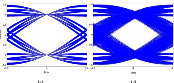
The sampling clock offset (SCO) is caused by the clock frequency difference between the transmitter DAC and the receiver ADC. For a SC system, SCO narrows down the eye of the eye diagram as shown in Fig. 2-3. Fig. 2-3(a) is an eye diagram
without SCO and Fig. 2-3(b) is that with 50 ppm SCO.
(a) (b)
Fig. 2-3 Eye diagram accumulated 50000 samples (12X oversample, raised cosine pulse shaping, and no AWGN) in a SC system (a) without SCO effect (b) with 50ppm SCO
For an OFDM system, SCO causes the rotation of the constellation be proportional with the subcarrier index and adds ICI as shown in Eqn. (2-1).
where SignalBB@RX is the received baseband signal in frequency domain, δ is SCO
normalized by the sampling frequency,ψ is the sampling phase offset, x(n) is the received signals in the time domain, X(p) is the transmitted signals in the frequency domain, N is the length of an OFDM and p is the sub carrier index. Fig. 2-4 shows the
ICI N N p j N p j p X N p p N ICI N p n j N p j p X N N nk j N p n j N np j p X N p n j p X N N nk j N p n j p X N N n N nk j n x Signal rotation phase N n N n term ICI k p N k p p k p N n N p N n RX BB
) ) 1 ( exp( ) 2 exp( ) ( ) sin( ) sin( 1 ) 2 exp( ) 2 exp( ) ( 1 ) 2 exp( ) ) ( 2 exp( ) 2 exp( ) ( ) ) ( 2 exp( ) ( 1 ) 2 exp( ) ) ) 1 ( ( 2 exp( ) ( 1 ~ 1 ) 2 exp( ) ) 1 ( ( 1 0 1 0 1 , 0 1 0 1 0 1 0 @ (2-1)ppm SCO disperses more than that of 50ppm. This is because higher SCO has higher ICI. Besides, after a long period of the transmission, the number of the received sample will be less or more than the transmitted one due to SCO.
(a) (b)
Fig. 2-4 Constellation rotation and dispersion (QPSK and no AWGN) caused by SCO in a OFDM system (a) with 50ppm SCO (b) with 500ppm SCO
There are two ways to model the effect of SCO. One is the resample based method and the other one is the fractional delay filter based method. The illustrations of these two methods are shown in Fig. 2-5. The resample based method requires the irreducible fractional of the added SCO. For example, if the added SCO is 50ppm, the irreducible fractional is 20001/20000. Then, the input signals are up-sampled by 20001 and are filtered by a low pass filter. Finally, the filtered signals are down-sampled by 20000 and a signal with 50ppm SCO is generated. The fractional delay filter method is like the time domain interpolation method of the SCO compensation. This method uses a fractional delay filter to insert SCO.
Fig. 2-5 Two methods of adding SCO (a) resample based method and (b) fractional delay filter based method
2.2.2 Effects of Carrier Frequency Offset
The carrier frequency offset (CFO) is caused by the mismatch between the transmitter mixer and the receiver mixer. Eqn.(2-2) shows how the signal of baseband (SignalBB) is carried into the radio frequency (SignalRF).
where „Re‟ is the real part of a signal, fc is the carrier frequency. Eqn.(2-3) shows how
the in-phase part of baseband in the receiver is generated.
) 2 sin( ) 2 cos( 2 exp Re @ t f Q t f I t f j Signal Signal c c c TX BB RF (2-2) ) 2 sin( ) 2 cos( )}] 2 ( 2 sin( ) 2 {sin( )} 2 ( 2 cos( ) 2 {cos( [ )] ) ( 2 cos( ) 2 sin( ) ( 2 cos( ) 2 cos( [ )] ) ( 2 cos( )) 2 sin( ) 2 cos( [( @ ft Q ft I f f ft Q f f ft I LP t f f t f Q f f t f I LP t f f t f Q t f I LP I c c c c c c c c c SignalBB RX (2-3)Where LP is a operation of a low pass filter and Δf is the CFO. By the same way, the quadrature-phase part is shown in Eqn. (2-4).
By combining Eqn.(2-3) and Eqn. (2-4), we can get the effect from CFO shown in Eqn.(2-5). This effect causes a rotated constellation in time domain
For the digital simulation, a normalized form is shown in Eqn.(2-6).
Where Δfd is the digital CFO normalized by the sampling frequency.
Then, we continue to drive the effect of CFO in frequency domain. An OFDM signal of the baseband is shown in Eqn. (2-7).
Where X(p) is the transmitted signal. Then, by adding CFO, we can get Eqn.(2-8).
) 2 cos( ) 2 sin( @ I ft Q ft Q RX BB Signal (2-4) ) 2 exp( ) 2 sin( ) 2 (cos( ) ( @ @ @ @ ft j Signal ft j ft Q j I Q j I Signal TX BB Signal Signal RX BB BB RX BB RX (2-5) ) ) ( 2 exp( ) ) ( 2 exp( ) 2 exp( ) 2 exp( @ @ @ @ @ n f j Signal n f f j Signal fnT j Signal ft j Signal Signal d TX B B s TX B B s TX B B TX B B R X B B (2-6) N n N np j p X N n x Signal N TX BB ) 1~ 2 exp( ) ( 1 ) ( 1 0 @
(2-7) N n n f j n x SignalBB@RX ( )exp( 2 d ) 1~ (2-8)The received X(p) is shown in Eqn.(2-9):
This effect of CFO in the frequency domain not only causes the constellation ratate but also adds ICI. A simulation of the effect of CFO is shown in Fig. 2-6. Fig. 2-6(a) is a result of a SC data block in the time domain and Fig. 2-6(b) is a result of OFDM system in frequency domain. The CFO effect between them is very different. In SC, each symbol suffers different phase rotation which is proportional to time index and the constellation becomes a cycle (QPSK). However, In OFDM, each subcarrier has the same phase rotation and ICI is also shown.
(a) (b)
Fig. 2-6 QPSK constellation rotation caused by CFO (a) a SC data block in time domain (b) an
ICI N f j j p X f N f N ICI n f j p X N N nk j n f j N np j p X n f j p X N N nk j n f j N np j p X N N n N nk j n f j n x Signal rotation phase common d d d N n d N n term ICI k p d N k p p k p d N n d N p N n d RX BB
)) 1 ( exp( ) 2 exp( ) ( ) sin( ) sin( 1 )) 2 exp( ) 2 exp( ) ( 1 ) 2 exp( )) ( 2 exp( ) 2 exp( ) ( )) ( 2 exp( ) ( 1 ) 2 exp( )) ( 2 exp( ) 2 exp( ) ( 1 ~ 1 ) 2 exp( )) ( 2 exp( ) ( 1 0 1 0 1 , 0 1 0 1 0 1 0 @ (2-9)2.3 AWGN
In a transmission, the thermal noise is the source of noise and its noise power spectral density (N0) is defined by Eqn.(2-10).
Where k is Stefan–Boltzmann constant and T is temperature in Kelvin scale. The thermal noise has almost flat power spectral density in frequency spectrum. Usually, additive white Gaussian noise (AWGN) is a model for the thermal noise. Signal to noise ratio (SNR) measures the quality of the received signal. For digital modulation,
Eb/N0 is usually adopted. Eb is the average energy per information bit. Besides, Eb/N0
is a normalization of SNR by spectral effectual (bit/s/Hz). The translation between SNR and Eb/N0 is shown in Eqn.(2-11) [20]:
Where fsymbol is the symbol rate, Es is the energy per symbol, B is the noise bandwidth,
M is the M-ary modulation and Crate is the coding rate. Another special condition, an
over sampling system, must be considered and are shown in Eqn.(2-12).
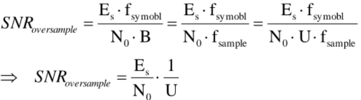
MHz Hz mW N / dBm -113.86 / dBm -173.86 K 298 K 10 1 10 1.38 C) (@25 K 298 K J 10 1.38 kT 3 23 -23 -0 (2-10) B f C (M) log N E C (M) log N E N E B N f E symbol 2 0 b 2 0 b 0 s 0 symbol s rate rate SNR N S SNR (2-11)
Where fsample is the sampling rate and U is the oversampling ratio. According to Eqn.
(2-12), for an over-sampling system, Es/N0 is U times as much as SNRoversample. An
example in Fig. 2-7 illustrates this condition. In this example, when adding 10dB noise power into a 4X-sampling system with signal power equal to 0 dB, Es/N0 is 16
dB and SNRoversample is 10 dB. The difference between Es/N0 and SNRoversample is 6dB,
equal to 10×log(4). However, there is usually a low-pass filter or a decimation filter in a transmission system. Fig. 2-8 shows the power spectrum density after passing a filter. Both Es/N0 and SNRfiltered becomes 16 dB. Fig. 2-9 is a summary. Hence, when
adding AWGN in an over-sampling system which contains a low-pass filter, the added noise power is required to be modified by using Eqn.(2-13)
Fig. 2-7 Illustration of SNR and Es/N0 in over-sampling ratio equal to 4 (U = 4)
U 1 N E f U N f E f N f E B N f E 0 s sample 0 symobl s sample 0 symobl s 0 symobl s oversample oversample SNR SNR (2-12) ) ( log 10 10 U SNR SNRadded required (2-13)
Fig. 2-8 Power spectrum density after passing a low-pass filter or a decimation filter
Fig. 2-9 Comparison of SNR and Eb/N0 in an oversampling system
2.4 Link Budget
Link budget is used to roughly estimate the required SNR of a receiver system at a certainly BER. Fig. 2-10 is a block diagram of the link budget of a receiver. A wireless receiver can be divided into three parts, the radio frequency (RF), the baseband, and the channel code as shown in Fig. 2-10. The radio frequency and the baseband introduce additional noises into the system and the channel code improves the system performance.
Fig. 2-10 Link budget of a receiver
There is a path loss (Ploss) between a transmitter and a receiver. The model of path
loss depends on the environment that signals pass through. For example, Eqn.(2-14) is a path loss model for free-space transmission [21]:
where Pr is the received power, Pt is the transmitted power, Gt is the antenna gain of
the transmitter, Gr is the antenna gain of the receiver, λ is the wave length of the
carrier, d is the distance between the transmitter and receiver. To replace with other path models, Eqn.(2-14) can be simplified into Eqn. (2-15).
2 2 4 d G G P P t r t r (2-14)
Where Rss is the receiver sensitivity. For defining a specification, the required Rss is
based on the following steps:
Define the required BER according to the requirement of application. Define the required Eb/N0 base on the performance of channel codes.
Translate Eb/N0 to SNRo according to the symbol rate, the bandwidth and
modulations
Consider the implementation loss (IMPloss) of baseband and the noise figure (Nf) of
the RF.
Calculate the thermal noise power based on Eqn. (2-10).
In short, the receiver sensitivity in dBm can be calculated by using Eqn.(2-16) is modified from [22]:
From the view of a baseband designer, the knowledge of the reasonable implementation loss is required. Usually, standards will list the receiver sensitivity and the requirement of BER or packet error rate (PER). We can speculate the reasonable implementation loss from that information. In the following, we take 802.15.3c [3] as an example and derive the reasonable implementation loss.
According to the 802.15.3c, the required PER is 0.08 at payload length equal to 214 bits in AWGN channel of SC mode; hence, the required BER can be calculated by using Eqn. (2-17). loss t r ss P P P R (2-15) ) ( ) log( 10 86 . 113 ideal -non dBm SNR N IMP B R o of Noise f loss power noise Thermal ss (2-16)
where n is the number of the transmitted bits. Thus, we can get the required BER is about 5.09×10⁻⁶. On the other hand, the required BER for OFDM mode is 1×10⁻⁶ [3]. Hence, we choose that the required BER is equal to 1×10⁻⁶. According to Fig. 2-11, the required Eb/N0 is about 3dB [23] for MCS 1 (QPSK (M = 2), code rate (Crate) =
1/2). Then, by using Eqn. (2-11), the required SNRo is also 3dB. The receiver
sensitivity of MCS1 is -50dBm [3]. By assuming the noise figure is 7 dB [24], the receiver SNRr after RF is about 24dB. Therefore, the reasonable implementation loss
is about 21dB.
Fig. 2-11 LDPC performance for MCS1, 2, 3 [23]
6 -16384 / 1 16384 ) 2 ( 10 5.09 ) 92 . 0 ( 1 92 . 0 ) 1 ( ) 08 . 0 1 ( ) 1 ( ) 1 ( ) 1 ( 14 BER BER BER BER PER BER n (2-17)
2.5 Summary
In this Chapter, channel models of 802.15.3c and DVB-T/H are introduced. Those channels can be divided into NLOS channel and LOS channel. The channel spectrum of LOS is usually more flat and can provide a better environment. In addition, the effects of the frequency offsets are also discussed. The frequency offsets causes the constellation rotate and introduce ICI. Finally, the method to calculate link budget in a communication system is shown. This can provide a rough speculation of the performance requirement.
Chapter 3
Data-path in a Baseband Receiver
This chapter introduces several data-paths used in the design of a baseband receiver. Different implementations and hardware complexity of those data-paths are compared.
3.1 Moving Sum Architecture
Maximum correlation and its recursive form shown in Eqn. (3-1) and Eqn. (3-2) is usually used in the symbol detection.
where x(n) is the received signal, N is the length of repeated signals, Ng is the length
of a repeated signal and P is the length of the detecting window. A moving sum architecture [25] implements the recursive form of the maximum correlation is shown in Fig. 3-1. The comparison of the direct implementation of Eqn. (3-1) and the moving sum architecture is shown in TABLE 3-1. The required multipliers and adders of the moving sum architecture are less.
1 0 * ~ 0 ) ( ) ( ) ( g N n P i N i n x i n x i k (3-1) ) ( ) ( ) ( ) ( ) ) 1 ( ) 1 (( )) 1 ( ) 1 (( ) ( ) 1 ( ) 0 ( ) 0 ( ) 1 ( ) ( ) 0 ( ) 1 1 ( ) 1 1 ( ) 1 ( ) 1 ( ) 2 ( ) 2 ( ) 1 ( ) 1 ( ) ( ) 0 ( ) 1 ( ) 1 ( ) 1 ( ) 2 ( ) 2 ( ) 1 ( ) 1 ( ) ( ) 0 ( ) 0 ( * * ) 0 ( * * ) 0 ( * * * * * * * * i k i k N i x i x N i N x i N x i k i k k k k N x x N N x N x N N x N x N x x N x x N x x k N N x N x N x x N x x N x x k g g k g g k g g g g (3-2)Fig. 3-1 Moving sum architecture [25]
TABLE 3-1 Comparisons of hardware complexity
Eqn.(3-1) Moving sum
Multiplier Ng 1
Adder Ng (summation) 2
Delay line N + 2Ng N + Ng
3.2 Delay Line
There are two ways to implement the delay line. One is the shift register based and the other is the memory based. Because a delay line is required to store and to push data at the same time, a dual port memory is a straightforward module to implement the delay line. However, the area complexity of a dual port memory is usually larger than that of a single port memory at the same the capacity. An architecture of the delay line using single port memory is shown in Fig. 3-2 [26]. This architecture uses two single port memories and each single port memory has half of the capacity of the delay line. These two single port memories are interlaced by read and write accessed. Hence, this architecture has the same function as a delay line.
Two design examples are shown in TABLE 3-2 and TABLE 3-3. In TABLE 3-2, the length of the delay line is very longer (a 8k delay line for DVB-T/H). Hence the implementation by single port memories has lower area compared to that of a dual port memory. However, in TABLE 3-3 which is a comparison of different implementations (802.15.3c) of memory, the length of the required memory is very
short. Therefore, the implementation by single port memories has no advantage. Besides, the implementation by logics and registers has the largest area in both design cases.
Fig. 3-2 Single port memory based delay line [26]
TABLE 3-2 Comparisons of different implementations of delay line (8K × 12) [10] [11] [12]
0.18um Process 8K shift register 8K dual port 8 × 1K single port
Area (mm^2) 5.56 1.56 1.04
TABLE 3-3 Comparisons of different implementations of memory (64 × 64)
65nm Process 64 (logic + register) 64 dual port 2 × 32 single port
Area (um^2) 47285 12280 17052
3.3 Differential Encoding [13] [26] [27]
The differential encoding is a method to reduce the required capacity of ROM. This method only stores difference between the successive values and the overhead is that it requires an additional accumlator. Fig. 3-3 is an example to record the continual pilot of DVB-T/H. The distribution pattern of differences is periodical. Hence, it only requires to record one period of the distribution pattern. The storage cost of the original method is 2301 (177 13) bits; in contrast, the storage cost of the differential
power-of-two. Hence, the implemented storage size becomes 512 (64 8) and is reduced by 77% [13] [26] [27].
Fig. 3-3 Differential encoding of continual pilot positions of DVB-T/H [13] [26] [27]
3.4 Complex Multiplier
The complex multiplier is a very common module in a baseband receiver. The traditional complex multiplier contains four multipliers and two adders. When considering the complexity of the area, the other architecture shown in Eqn.(3-3) is proposed by [28] [29]. An illustration of these two architectures is shown Fig. 3-4. The modified complex multiplier has a common term and it reduces a multiplier. Comparisons of two architectures are shown in TABLE 3-4. The modified one has lower complexity but its critical path is longer.
j d c b b a d d c b b a c j bd bc bd ad bc bd bc ac j bc ad bd ac dj c bj a ) ) ( ) ( ( ) ) ( ) ( ( ) ( ) ( ) ( ) ( ) ( * ) ( (3-3)
(a) (b)
Fig. 3-4 Architectures of complex multiplier (a) 4 „×‟ and 2 „+‟ (b) 3 „×‟ and 5 „+‟ [28][29]
TABLE 3-4 Comparisons of different complex multiplier
Original Modified [28][29]
Multiplier 4 3
Adder 2 5
Critical path 1 Multiplier, 1 Adder 1 Multiplier, 2 Adder
3.5 Loop Filter
In a synchronization loop, a loop filter is used to suppress noise and makes the freed back loop stable. A simple loop filter shown in Fig. 3-5 is usually used in the baseband receiver and its detail description is reported by [25] [30]. C1 and C2 are
adjustable and can control the convergence speed and the stability of the steady state. Fig. 3-6 shows different tracking curves at different loop filter coefficients for the CFO loop used in a 802.15.3c baseband receiver. To reduce the hardware complexity,
be replaced by wire shifting.
Fig. 3-5 Architecture of a loop filter [25] [30] on the CFO loop
Fig. 3-6 Tracking curves of different filter coefficients for CFO loop in a 802.15.3c baseband receiver
The detail analysis of this loop filter is reported by [30]. To quickly select a suitable set of coefficients, C1 and C2 can be decomposed into Kc and Kd as shown in Eqn.(3-4).
Different combinations of Kc and Kd of trucking curves are shown in Fig. 3-7.
d c c K K C K C 1 1 1 2 1 (3-4)
(a) (b)
(c) (d)
(e) (f)
Fig. 3-7 Different combinations of Kc and Kd (a) Kd = 1, (b) Kd = 4, (c) Kd = 8, (d) Kd = 16, (e) Kd = 32, (f) Kd =64,
According to these trucking curves, we can roughly figure out than Kc controls
the convergence and the stability in the steady state and Kd controls the level of
damping. The applicable set of Kd is {4, 8, 16, 32, 64}. When deciding the value of Kd,
it is recommend to select from big to small number of the set. Deciding the value of
Kc relates to the average value of estimation in open loop (Ve) and the compensation
range (Cr). Kc can roughly be set to 10~100 times Ve/Cr (This paragraph is an
empirical rule).
3.6 CORDIC
The coordinate rotational digital computer (CORDIC) [31] [32] [33] is an algorithm to compute the trigonometric functions. The basic idea of this algorithm is as follows:
where A is a complex number and B is A rotated by θ. Then, we can translate Eqn. (3-5) into a matrix form:
Then, Eqn.(3-6) can be modified to:
Assume θ is composed of severaland tan ()s are power of two
) exp(j A B (3-5) I R Matrix Rotation I R A A B B sin( ) cos( ) ) sin( ) cos( (3-6) I R Matrix Rotation I R A A B B tan( ) 1 ) tan( 1 ) cos( (3-7)
Finally, the rotation by θ can be replaced with several micro angles and the implementation only requires adder and wire shifting. For baseband applications, the additional gain is not a problem because the equalizer will compensate this gain.
Two architectures are used in the implementation of CORDIC and they are the folding and the unfolding architecture shown in Fig. 3-8 [34] [35]. The comparison of these two architectures is shown in TABLE 3-5. In sort, the folding architecture has lower complexity but it required an additional N times clock rate. The unfolding architecture has a longer critical path but it can use pipeline architecture to speed up the computation.
(a) (b)
Fig. 3-8 Implementation of CORDIC (a) folding architecture (b) unfolding architecture [34] [35] i i N i i noise
tan( ) 2 1 0 (3-8) noise A A B B I R Matrix Rotation N N Matrix Rotation Matrix Rotation gain Addtional n I R 2 1 2 1 1 2 2 1 1 2 2 1 ) cos( ) cos( ) cos( 1 1 1 1 0 0 2 1 (3-9)TABLE 3-5 Comparisons of implementations of CORDIC
Folding Unfolding
Adders 3 3 × N
Shifter Barrel shifter Wire shifting Critical path 1 Barrel shifter, 1 Adder N Adders
Clock rate
One additional N times Clock rate
The same clock rate as the baseband Note: N is the number of the CORDIC stages
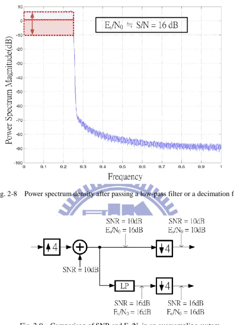
3.7 Removing DC error
In the hardware design, a suitable truncation scheme reduces the hardware complexity and keeps the performance. In the 2‟s complementary system, the truncation makes both a positive number and a negative number become smaller. Hence, the received data has a DC gain error after truncation. In an OFDM system, the received data will transfer into the frequency domain; therefore, the DC subcarrier will suffer from a large performance loss due to the truncation. Fortunately, the DC subcarrier usually does not carry any information (a Null subcarrier) in most OFDM system to prevent the re-radiation or leakage of a local oscillator (LO). A simple and easy method reported by [36] can remove the DC error with a little overhead.
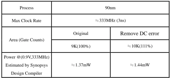
Fig. 3-9 shows a hardware design example of the removing DC error. The example is a Multiply-Add function in an interpolator. Fig. 3-9 (b) is a version of the removing truncation DC error. Two constant adders are required according to the method. Besides, the Multiply-Add function is replaced by a DesignWare IP [37], „DW_02_prod_sum1‟. Fig. 3-10 is a simulation result of removing truncation DC error. It shows the DC error in the Fig. 3-10 (a) can be removed. Finally, the hardware
complexity comparisons are listed in TABLE 3-6. The design example is a Cubic Lagrange intepolator [8] [9]. The design overhead of removing DC error is that the gate counts are increased by 11%.
(a) (b)
Fig. 3-9 Hardware implementation of Multiply-Add (a) original (b) removing DC error version
(a) (b)
TABLE 3-6 Synthesis comparisons of an interpolation with and without the removing DC
Process 90nm
Max Clock Rate ≒333MHz (3ns)
Area (Gate Counts)
Original Remove DC error
9K(100%) ≒10K(111%)
Power @(0.9V,333MHz) Estimated by Synopsys
Design Compiler
≒1.37mW ≒1.44mW
3.8 Fast Fourier Transform
In an OFDM receiver, a Fast Fourier Transform (FFT) unit is required to transform data form the time domain to frequency domain. The output order of an FFT has two kinds as shown in Fig. 3-11. The normal order is a general order of FFT output. However, in standards [1] [3], the positions of pilots are recorded in the reversed order. It is important to make sure what kind order is used in standards.
(a) (b)
Fig. 3-11 Output order of FFT (a) normal order (b) reversed order
Pipeline-based architecture [38] [39] [54] and memory-based [40] [41] architecture are widely used in the implementation of FFT. The comparisons of these two architectures are shown in TABLE 3-7. The memory-based architecture can be regarding as folding form of the pipeline architecture. Hence, the memory-based one
has low complexity but it require more clock cycles to accomplish process. The pipeline-based one usually can operate at a higher frequency by pipelining. When considering the application of OFDM system, the successive data input to FFT unit is an important issue. The memory-based one need an extra input buffer for temporarily storing the input data but the pipeline-based one does not require. In the other hand, the order of output of pipeline-based one is not regular; hence, it requires a reorder buffer. In contrast, the memory-based one can reuse the internal memory.
TABLE 3-7 General comparison of FFT architectures
Pipeline-based (SDF) [38] [39] [54] Memory-based [40] [41] Complexity × ○ Speed ○ × Successive Data in ○ ×
(require a input buffer)
Reorder ×
(require a reorder buffer)
○
(reuse the internal memory)
Fig. 3-12 2K/4K/8K FFT [52] with single path delay feedback (SDF) [38] [39] [54] and Radix-2/4/8 [53]
Fig. 3-12 is a 2K/4K/8K FFT (a work of Syu-Siang Long [52]) adopted in DVB-T/H receiver. This FFT uses single path delay feedback (SDF) [38] [39] [54] which is a pipeline-base architecture and combines Radix-2 and Radix2/4/8 [53]. A reorder buffer is used to transform the output order. It can operate at 40MHz clock and process 2K, 4K, and 8K FFT operations.
3.9 Summary
Several implementation methods of a delay line are discussed in this chapter. The length of delay can roughly decide how to implement a delay line. When the length is shorter, the complexity of the implantation of dual port memories is comparable with that of single port memories. On the contrast, when the length is longer, the implementation by single port memories has lower complexity. Algorithms of a baseband receiver require trigonometric modules such as cosine, sine, and arc-tangent. CORDIC algorithm can calculate those functions and has a good ability for reusing. Two architectures of CORDIC are compared and the adoption of these two architectures depends on the receiver architecture. Besides, the truncation operation is usually used to reduce the hardware cost but a DC error is generated in a 2‟s complementary system. This error has large influence on the DC subcarrier of an OFDM system. A removing DC error technique [36] is introduced. The method can eliminate the DC error with smaller overhead. Two architectures of FFT are compared. The memory-based architecture has lower complexity but requires more clock cycles. The pipeline-based architecture can operate at high frequency but an extra reorder buffer is required.
Chapter 4
OFDM Baseband Receiver for
DVB-T/H
This chapter shows the proposed DVB-T/H receiver. First, an introduction of DVB-TH standard is presented and the proposed architecture for a DVB-TH receiver is shown. Then, several schemes are proposed to reduce the hardware complexity and the power consumption. Finally, the implementation results are shown.
4.1 Introduction of DVB-TH
Digital video broadcasting terrestrial and handheld (DVB-T/H) [1] [2] are proposed by European Telecommunications Standards Institute (ETSI) to transmit digital TV signal. DVB-T/H defines three different bandwidths, 6, 7 and 8MHz for different areas and countries. In Taiwan, the standard of digital TVs adopts 6MHz DVB-T. Fig. 4-1 shows the DVB-T/H transmitter block diagram [1] [2]. The DVB-T/H adopts two level channel codes, Reed Solomon code and convolution code. Reed Solomon code has a better ability against bust errors and convolution code is more suitable for random errors. Hence, these two codes cooperate well.
The DVB-T/H standard adopts orthogonal frequency division multiplexing (OFDM). In the DVB-T/H, there are three symbol lengths, 2048 (2K Mode), 4096(4K Mode) and 8192 (8K Mode) and four guard interval (GI) lengths which are used for
transmission parameter signaling (TPS) pilots are inserted in the frequency domain. The continual pilots have fixed position, the scattered pilots change their position every OFDM symbols and the TPS is used to transmit system parameters. The data subcarriers can use several different constellation schemes like, quadrature phase-shift keying (QPSK), 16 quadrature amplitude modulation (QAM) and 64QAM. TABLE 4-1 is a summary of the specification of DVB-T/H.
Fig. 4-1 The DVB-T/H transmitter block diagram [1] [2]
TABLE 4-1 Specification of DVB-T/H [1] [2]
Bandwidth (MHz) 6 7 8 Samping Preiod (us) 7/48 1/8 7/64
FFT Length, 2K,4K,8K Used Subcarriers 1705, 3409, 6817
Guard interval 1/4, 1/8,1/16,1/32 Modulation QPSK, 16QAM, 64QAM
4.2 Baseband Receiver Architecture
Fig. 4-2 shows the block diagram of the DVB-T/H baseband receiver. In the receiver, the Mode/GI/Symbol detection, the carrier synchronization, the sampling clock synchronization and the channel estimation (inner receiver) are designed and implemented into RTL level. The soft demapper, the interleaver, and the soft Viterbi decoder (outer receiver) are behavior models which are used to measure the receiver performance. The hardware implementation contains two clock rate domains. One is 4X clock rate and the other is 1X clock rate. The derotator, the interpolator and the FFT operate at 4X clock rate. On the other hand, the Mode/GI/Symbol detection, the channel estimation, the integer CFO (ICFO) estimation and the SCO and residual CFO (RCFO) estimation [5][6][7] work at 1X clock rate.
The demodulation flow has two stages: the acquisition stage and the tracking stage. In the acquisition stage, the receiver detects the transmission Mode and the GI length, finds the OFDM symbol boundary, compensates the fractional CFO (FCFO) and estimates ICFO. Then, the demodulation flow enters into the tracking stage. In the tracking stage, the receiver tracks SCO and RCFO. After getting into the steady state, the receiver detects the scattered pilot mode, does channel estimation, equalization and demaps the constellation into bits stream.
The goal is to design a low power and low complexity baseband receiver. The following is the summary of the adopted schemes to reduce the power consumption or the hardware complexity:
The Phase prediction scheme reduces the operations of phase accumulators during GI period. (Low power)
ability. (Low power)
The Differential encoding scheme of continual pilots positions reduces the storage cost.(Low complexity)
The Mode/GI/Symbol detection and the channel estimation share the same memory bank.(Low complexity)
The integer CFO (ICFO) estimation and the residual CFO (RCFO) and SCO estimation share the same memory module. (Low complexity)
Fig. 4-2 The DVB-T/H receiver architecture
4.3 GI Detection [10] [11] [12]
The Mode/GI detection algorithm [42] adopts the cyclic prefix (CP) based correlation algorithm to identify the symbol mode. Eqn.(4-1) is the maximum correlation (MC) [6]:
1 32 0 * ) ( ) ( ) ( Nsc i MC n r n i r n i Nsc x (4-1)where r(n) is the received signal, Nsc is the number of sub-carriers and Nsc/32 is the shortest guard interval length. The correlation result xMC(n) will form a peak or
plateau if the tested mode equals to the transmitted symbol mode. However, defining the threshold and detecting the plateau are difficult due to glitches. Eqn.(4-2) is a modified form of Eqn.(4-1) called the normalized maximum correlation (NMC) [43] [44]:
The denominator denotes the power of received signal r(n) and is employed to normalize to “1”. Unlike MC method, NMC method has more flat plateau and is easy to detect the GI length; however, the NMC method requires division operation.
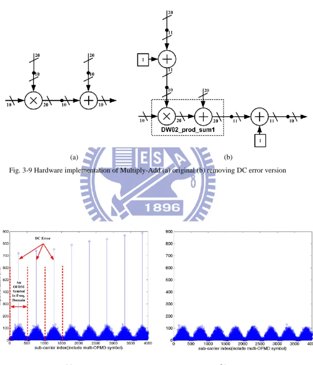
To reduce the division operation of NMC, the plateau threshold is defined as „Th‟ as
given by Eqn.(4-3). Then, the GI detection equation can be modified as shown in Eqn.(4-4). A division operation is removed by moving the denominator to the right side and adopting a pre-determined threshold, Th. Moreover, the square-root operation
in the absolute operation of a complex number is also not required by squaring both sides.
1 32 0 * 1 32 0 * ) ( ) ( ) ( ) ( ) ( Nsc i Nsc i NMC i n r i n r Nsc i n r i n r n x (4-2) h NMC NMC plateau if x n T n x( ) ( ) (4-3)Determine an accurate detection is important in reducing the detection error. Using low threshold, the non-plateau region will be regarded as a plateau region and it causes incorrect GI length detection. Using high threshold, glitches on the plateau will decrease the estimated plateau length and cause incorrect GI detection. Fig. 4-3 and Fig. 4-4 are GI detection error rate simulations results for 2k and 8k mode. In simulation results, the detection rate at 8K mode is better than that at 2K mode. This is because 8K mode has the longest symbol length. Except the case of 1/32 GI length, the detection error rate has similar behavior at the low and high threshold. In the case of 1/32 GI length, at low threshold, miscalculated plateau decreases the GI detection error rate. At high threshold, due to the decision boundary of 1/32 GI case, the decreased plateau length does not cause the detection error in these simulations. For detection error rate to be lower than 0.01, the threshold is chosen to be 0.5. In 1/32 GI and 2K mode case, the performance is very close to 0.01. The multiplication in Eqn.(4-4) can be replaced with displacement of wiring in the hard implementation.
0 ) ( ) ( ) ( ) ( ) ( 2 1 32 0 * 2 2 1 32 0 *
Nsc i h Nsc i i n r i n r T N i n r i n r (4-4)Fig. 4-3 GI detection error rate vs. threshold under 8K transmission mode, AWGN level = 5dB and Rayleigh channel [1] [2]
Fig. 4-4 GI detection error rate vs. threshold under 2K transmission mode, AWGN level = 5dB and Rayleigh channel [1] [2]
4.4 CFO and SCO synchronization
OFDM systems are sensitive to mismatches of carrier and sampling frequencies between transmitter and receiver. These mismatches cause two effects: phase rotation and intercarrier interference (ICI). CFO causes the constellation of an OFDM symbol to rotate by a common phase; on the other hand, the phase rotation caused by SCO is proportional to the subcarrier index [5][6]. In addition, the frequency offset breaks the orthogonality of OFDM systems; as a result, the transmitted data on a subcarrier is interfered by other subcarrier and causes the degradation of performance.
To avoid ICI and to keep the phase of the constellation fixed, the receiver needs to compensate the frequency offset. The CFO is composed of fractional CFO (FCFO) and integral CFO (ICFO) in an OFDM system. A three steps method for the carrier frequency synchronization (one pre-FFT and the other post-FFT) is reported by [5] [6] [7]. First, at the symbol boundary detection, the result of delay correlation is also used for estimating FCFO [43]. In the second step, ICFO is estimated in frequency domain by using pilots. However, the FCFO estimation cannot be estimated perfectly. A residual CFO (RCFO) still remains. Hence, a RCFO and SCO estimation [5] [6] [7] in the frequency domain is used to keep tracking RCFO and SCO at every OFDM symbol in the final step.
This work adopts the carrier frequency and sample clock synchronization [5] [6] [7]: ) ( 2 1 ) / 1 ( 2 1 , 2 , 1l l g N N f
Where fΔ is the estimated CFO, tΔ is the is the estimated SCO, k is the number of
subcarrier, N is the length of the OFDM, Ng is the length of guard interval, C1 is the
positive continual pilot set, C2 is the negative continual pilot set, and Z is product of
subcarriers of successive OFDM symbols. The architecture of the RCFO and SCO estimation is shown in Fig. 4-5. The „tan-1’ module calculates the angle of a complex number and this module adopts the CORDIC algorithm [31]. To smooth the RCFO and SCO estimation, the loop filters [30] are added into the synchronization loops. The coefficients of the loop filters are designed as power-of-twos; therefore, the multipliers can be replaced with wire-shifting.
Fig. 4-5 Memory sharing architecture for ICFO, residual CFO (RCFO) and SCO estimation
) ( 2 / 1 ) / 1 ( 2 1 , 2 , 1l l g N k N t
![Fig. 2-2 802.15.3c channel models provided by [18] and only print the first 100 samples](https://thumb-ap.123doks.com/thumbv2/9libinfo/8465856.183347/22.892.146.720.126.736/fig-c-channel-models-provided-print-samples.webp)

![Fig. 3-3 Differential encoding of continual pilot positions of DVB-T/H [13] [26] [27]](https://thumb-ap.123doks.com/thumbv2/9libinfo/8465856.183347/38.892.132.748.240.758/fig-differential-encoding-continual-pilot-positions-dvb-t.webp)
![Fig. 4-4 GI detection error rate vs. threshold under 2K transmission mode, AWGN level = 5dB and Rayleigh channel [1] [2]](https://thumb-ap.123doks.com/thumbv2/9libinfo/8465856.183347/55.892.151.712.286.963/detection-error-threshold-transmission-awgn-level-rayleigh-channel.webp)
