國
立
交
通
大
學
光電系統研究所
碩 士
論
文
氧含量對非晶態透明半導體銦鋅錫氧薄膜電晶
體特性之研究
Study on the effect of oxygen incorporation on amorphous
Indium Zinc Tin Oxide transparent thin film transistors
研 究 生:劉玫諍
指導教授:劉柏村 教授
林建中 教授
氧含量對非晶態透明半導體銦鋅錫氧薄膜電晶體特性之研究
Study on the effect of oxygen incorporation on amorphous Indium
Zinc Tin Oxide transparent thin film transistors
研 究 生:劉玫諍 Student:Mei-Jeng Liu
指導教授:劉柏村 教授 Advisor:Prof. Po-Tsun Liu
林建中 教授
Prof. Chien-Chung Lin
國 立 交 通 大 學
光 電 系 統 研 究 所
碩 士 論 文
A Thesis
Submitted to Institute of Photonic System College of Photonics
National Chiao Tung University in partial Fulfillment of the Requirements
for the Degree of Master
in
Photonic System August 2013
Tainan, Taiwan, Republic of China
I
氧含量對非晶態透明半導體銦鋅錫氧薄膜電晶體特性之研究
學生: 劉玫諍 指導教授: 劉柏村 教授
林建中 教授
國 立 交 通 大 學
光電系統研究所
摘要
近年來非晶態透明導電膜因具備高透光性與高電流驅動特性而受到矚目,而
為了減少材料中稀有金屬的使用及提高載子遷移率的需求,我們研究了新材料
indium-zinc-tin oxide(IZTO),對非晶態的 IZTO 電晶體進行電特性與材料特
性的探討與分析。a-IZTO 的光學能隙高達 3.6eV 以上,僅會吸收波段小於
360nm 的紫外光,在可見光的波段具有高穿透性,再者 a-IZTO 在製程上可達
到低退火溫度(300℃)與具有高載子移動率等優點,所以極有潛力成為下一代
的主流顯示技術。
本研究中,探討不同氧含量的薄膜做為主動層對元件特性的影響,由實驗結
果得知,微量的氧能修補薄膜內的缺陷進而達到優化的效果,然而薄膜內的缺
陷態卻會隨著氧含量的增加而增加,而載子移動率隨之下降,再者,此實驗中
II
優化的元件在經過低溫退火後的最高載子移動率可達 15 cm
2/V.s~ 20cm
2/V.s。
為了能進一步應用在平面顯示器上,我們將此最佳化的條件成功轉移於具可撓
曲淺力之超薄(0.13mm)玻璃基板上,實驗結果顯示電晶體依舊能維持不錯的元
件特性(載子移動率-12~13 cm
2/V.s)。a-IZTO 具有高載子移動率與應用於可撓
曲超薄玻璃基板之優勢,此研究的發展將極具淺力。
III
Study on the effect of oxygen incorporation on amorphous Indium
Zinc Tin Oxide transparent thin film transistors
Student :
Mei-Jeng Liu
Advisors : Prof. Po-Tsun Liu
Prof. Chien-Chung Lin
Institute of Photonic System
National Chiao Tung University, Tainan, Taiwan
Abstract
Recently, the thin film transistors (TFTs) with transparent amorphous
con-ductive thin film as active layer perform higher mobility and better reliability than
conventional hydrogenated amorphous silicon TFT (a-Si: H TFT). In addition, the
uniformity of a-IGZO TFT is also superior to low temperature polycrystalline
sili-con TFT (LTPS TFT). However, the usage of the rare element(Ga) and further
en-hancement of device mobility will be an important issue for the long-term
amor-IV
phous In-Zn-Sn-O thin film transistors (a-IZTO TFTs). We investigated the effect
of oxygen incorporation on a-IZTO thin film transistors. For the devices with
dif-ferent oxygen flow rate incorporation, the small quantity of oxygen can repair
de-fects and optimize the characteristic, however, the trap states increase when oxygen
flow rate increases, leading to the decreasing mobility. Moreover, the mobility of
the optimized devices after annealing has reached 15 cm
2/V.s~ 20cm
2/V.s. For the
application of flat panel displays, we have successfully transferred the optimized
device from Si wafer to the ultra thin glass (0.13mm) which has bending potential.
Devices on ultra thin glasses have stable basic electrical characteristics and their
mobilities were also comparable (12~13 cm
2/V.s). With the advantages of high
mobility and ultra thin glass, these results show the future application potentials of
V
Acknowledgements (誌謝)
首先要感謝劉柏村教授建立了一個資源豐富的研究環境,除了設備完善讓我們可以有 世界級的研究成果,高水準的師資與研究團隊可以隨時與世界頂尖研究成果爭雄,實驗 室注重英文能力等精神也讓我們不忘踏出關門研究的階段,培養國際化的視野,成為更 全方位的人才,可以在未來為校爭光,回饋培育我們的社會,另一方面也感謝林建中教 授給我許多指導與建議,兩年的碩士班生涯令我受益良多。 接著要感謝我的夥伴豐榮、韋勳、永翰,在無塵室裡、量測機台邊共度無數時光。他 們在我的實驗過程中給了我許多鼓勵與建議,也能在擁有得來不易令人欣慰的研究成果 時與他們共享。還要感謝我的學長們立峯、光廷、治翔、揚順、智翔,不時的給予關心 與指點,特別是傅治翔學長,謝謝你在我遇到困難的時候,不遺餘力的幫忙與指導,點 點滴滴銘記在心; 還有同年同月同日生的夥伴兼學長-智翔,在初進實驗室什麼都不懂之 時,教了我許多經驗與知識,也讓我在研究所生涯中多了一位知心的朋友。另外是實驗 室很有義氣的學弟妹們于德、昱達、忠民、為量、鈞罄、人傑、郁嘉,謝謝你們在我需 要幫忙時,皆義不容辭的提供協助。 還有台南 417 共同研究室的夥伴們,在與大家一起修課的那半年裡,是我一段很美好 的回憶,每次與你們相聚,總能使我開懷大笑,相信畢業之後雖然分散各地,大家的友 誼依舊能長存的,也祝大家工作順利、前程似錦。再來是我的男朋友-晏增,在這兩年 裡,謝謝你在我身邊的陪伴與鼓勵,很高興能與你分享這點點滴滴的回憶,碩士生涯也 因為你而變得更加豐富。 最後最重要的,我要感謝我的父母劉玉進先生、史雅英小姐,謝謝你們的養育之恩、 栽培之情,與不離不棄的陪伴,在即將邁入社會之際,我會盡一切努力報答你們,作一 個能讓你們感到欣慰與驕傲的女兒。VI
Table of Contents
Abstract (Chinese)... I
Abstract (English) ... III
Acknowledgements ... V
Table of Contents ... VI
Figure Captions ... VIII
Table Captions ... X
Chapter 1
Introduction ... 1
1.1General Background... 1
1.2Amorphous oxide semiconductors ... 3
1.2.1 Introduction of Amorphous Oxide Semiconductors ... 3
1.2.2 Material properties of zinc oxide (ZnO) ... 3
1.3Motivation ... 4
1.4 Thesis Organization ... 5
Chapter 2
Experimental Procedures ... 7
2.1Fabrication flow of thin film transistors ... 7
VII
Chapter 3
Results and Discussion ... 14
3.1The effects of oxygen flow rate and channel thicknesson a-IZTOTFTS ... 14
3.1.1 Characteristic analysis of a-IZTO TFTs with different RF sputtering power ... 14
3.1.2 Characteristic analysis of a-IZTO TFTs with different oxygen flow rate ... 16
3.1.3 Characteristic analysis of a-IZTO TFTs with different channel thickness ... 18
3.1.4 Summary ... 18
3.2 Reliability Analysis of a-IZTOTFTS ... 19
3.2.1 Electrical reliability analysis under gate bias stress ... 19
3.2.2 The photosensitivity analysis ... 22
3.2.3 Summary ... 24
3.3 Application of a-IZTO TFTs for ultra-thin glass panel ... 24
3.3.1 Introduction ... 24
3.3.2 Device structure ... 25
3.3.3 Electrical characteristic analysis ... 25
3.3.4 Electrical reliability analysis under gate bias stress ... 26
3.3.5 Summary ... 27
Chapter 4
Conclusion ... 40
4.1Conclusions ... 40 4.2Future work ... 41Reference ... 42
VIII
Figure Captions
Chapter 1 Introduction
Fig.1-1 Flexible transparent TFTs (TIFTs) (a) A photograph of the flexible TIFT sheet bent at
R = 30 mm. The TIFT sheet is fully transparent in the visible light range (b) a photograph of the flexible TIFT sheet. The transparent TFT devices are made visible by adjusting the angle of the illumination ... 6
Fig.1-2 Schematic orbital drawing of electron pathway (conduction band bottom) in
conventional silicon-base semiconductor and ionic oxide semiconductor. ... 6
Chapter 2 Experimental procedures
Fig.2-1 The experimental flow path ... 13
Fig.2-2 a-IZTO TFT device structure ... 13
Chapter 3 Result and discussions
Fig.3-1 The AFM results of 30nm IZTO film roughness for oxygen flow rate (a) 0 sccm, (b)
0.1 sccm, (c) 0.5 sccm, (d) 1 sccm, (e) 1.5 sccm, after annealing process ... 28
Fig.3-2 The SEM results of 30nm a-IZTO film surface for oxygen flow rate (a) 0 sccm, (b)
0.1 sccm, (c) 0.5 sccm, (d) 1 sccm, (e) 1.5 sccm, after annealing process ... 28
Fig.3-3 XRD pattern of 30nm a-IZTO thin film for five different oxygen flow rate after
annealing process ... 29
Fig.3-4 Transfer characteristics of three different RF sputter power with the same thickness
30nm and consistent oxygen flow rate (0.5 sccm) ... 30
Fig.3-5 Relation between deposition rate (nm/min) and oxygen flow rate(sccm) with power
70w ... 30
Fig.3-6 electrical performance with different oxygen flow rate in (a) 10nm (b) 30nm (c) 50nm.
... 31
Fig.3-7 The overall characteristic of different oxygen flow rate with thickness (a) 10nm (b)
30nm (c) 50nm. ... 31
Fig.3-8 Relation between trap state and oxygen flow rate(sccm) ... 32
Fig.3-9 transfer characteristic of a-IZTO TFTs with oxygen flow rate (a) 0 sccm (b) 0.1 sccm
IX
Fig.3-10 transfer characteristic of the oxygen flow rate 0.5 sccm with different thickness... 33
Fig.3-11 Threshold voltage (Vth) shift of 10nm a-IZTO TFT devices under (a) positive gate
bias stress (PGBS) and (b) negative gate bias stress (NGBS) for 2000 seconds. ... 33
Fig.3-12 Subthreshold swing (S.S.) shift of 10nm a-IZTO TFT devices under (a) positive gate
bias stress (PGBS) and (b) negative gate bias stress (NGBS) for 2000 seconds ... 33
Fig.3-13 the logarithmic time dependence of Vth with the stretched-exponential fitting curve
... 34
Fig.3-14 (a) the 30nm film transmittance with different oxygen flow rate transparent through
the visible spectrum. (b) the relationships between (αhν)2 and the photon energy (h ν) ... 34
Fig.3-15 Transfer curves of devices with oxygen flow rate (a) 0 sccm, (b) 0.1 sccm, (c) 0.5
sccm, (d) 1 sccm, (e) 1.5 sccm under visible light illumination ... 35
Fig.3-16 back light spectrum with intensity. ... 35
Fig.3-17 Threshold voltage (Vth) shift of (a) light illumination for 2000 seconds without
applying bias (b) recovery mesurement at 1 hour, 3 hour, and 6 hour after the light illumination. ... 36
Fig.3-18 (a) Threshold voltage (Vth) shift of light illumination for 2000 seconds with gate bias
-25V (b) the logarithmic time dependence of Vth with the stretched-exponential fitting curve
... 36
Fig.3-19 Structure of a-IZTO TFT fabricated on ultra thin glass ... 37
Fig.3-20 The (a) side view and (b) top view of a-IZTO TFT fabricated on ultra thin glass. ... 37
Fig 3-21 Electrical performance of the device with oxygen flow rate 0.1 sccm. ... 38
Fig.3-22 Electrical performence of a-IZTO TFT devices under (a) positive gate bias (25V)
stress (PGBS) and (b) negative gate bias (-25V)stress (NGBS) for the time duration of 2000 seconds ... 38
Fig.3-23 Hysteresis in transfer characteristics observed between forward (VG = -40Vto 40 V)
X
Table Captions
Table 3-1 elemental composition of 30nm a-IZTO thin film examined by XPS analysis ... 29
Table 3-2 Parameter of three different RF sputter power with the same thickness 30nm and consistent oxygen flow rate (0.5 sccm) ... 30
Table 3-3 Parameters of trap state of different oxygen flow rate with the thickness 10nm ... 32
Table 3-4 Correlative parameters of stretched-exponential fitting curve ... 34
Table 3-5 optical band-gaps for 30nm a-IZTO thin film with different oxygen flow rate ... 35
Table 3-6 Correlative parameters of stretched-exponential fitting curve ... 36
Table 3-7 Comparison of 10nm a-IZTO device on with five different oxygen flow rate in mobility (cm2/V.s) ... 37
1
Chapter 1
Introduction
___________________________________________________________________________
1.1 General Background
Thin-film transistors (TFTs) are fundamental building blocks and play a domination
role for state-of-the-art microelectronics, such as flat-panel displays and system-on-glass. Furthermore, the fabrication of low-temperature TFTs will allow flexible large-area electronic devices to be developed. As shown in Fig.1-1,these devices are flexible, lightweight, shock resistant and potentially affordable—properties that are necessary for large, economic, high-resolution displays, wearable computers and paper displays [1]. Research on amorphous
semiconductors started in 1950s to seek appropriate materials. And hydrogenated amorphous silicon (a-Si:H) is the first material which can control carrier concentration by impurity dop-ing as in crystalline. Nowadays, the a-Si:H which is used widely in active-matrix flat-panel display (AMFPD) circuits. However, the growth of high-end commercial market with high-resolution such as ultra definition (2000x4000), high frame rate(>120Hz), and size larger than 50 in. necessitates the development of high-performance transistors(with field-effect mobility >3cm2 /V.s).[2]
2
Hydrogeneated amorphous silicon thin film transistor (a-Si:H TFT) is not an appropriate device for next generation displays on account of its low mobility (< 1 cm V-1 s-1 ), photo sen-sitivity (low band gap about 1.7ev) and rather high deposition temperature(~400℃). On the other hand, polycrystalline silicon (poly-Si) TFT which has high mobility (> 100 cm V-1 s-1 ) suffers from a problem with the variation of electrical properties due to grain ry[ 3-4].The mobility of a-Si:H (~1 cm2(Vs)-1) is much smaller than that of single crystalline Si (~200 cm2(Vs)-1) due to the intrinsic chemical bonding nature. The average carrier trans-portation paths in covalent semiconductors, such as a-Si:H, consist of strongly directive sp3 orbital. The bond angle fluctuation significantly alters the electronic levels, causing high density of deep tail-states, as shown in Fig.1-2 [ 5]. In contrast, degenerate band conduction and large mobility (>10cm2/V.s) are possible in amorphous oxide semiconductors (AOSs) containing post-transition-metal cations. These features are completely different from those of the covalent semiconductors. Figure 1-2 illustrates the carrier transport paths in AOSs. The bottom of the conduction band in the oxide semiconductors that has high ionicity is primarily composed of spatially spread metal ns orbitals with isotropic shape (here n is the principal quantum number), and direct overlap among the neighbouring metal ns orbitals is possible. The magnitude of this overlap is insensitive to distorted metal–oxygen–metal (M–O–M) chemical bonds that intrinsically exist in amorphous materials. Therefore, AOSs exhibit Hall-effect mobilities similar to those of the corresponding crystalline phase, even if they are
3
formed at room temperature. These carrier transport properties are unique to oxide semicon-ductors, and are not seen in covalent amorphous semiconductors such as a-Si:H[1].
1.2 Amorphous Oxide Semiconduvtors
1.2.1 Introduction of Amorphous Oxide Semiconductors
Amorphous oxide semiconductors (AOSs) are expected as new channel materials in thin-film transistors (TFTs) for large-area and/or flexible flat-panel displays and other gi-ant-microelectronics devices. So far, many prototype displays have been demonstrated in these four years since the first report of AOS TFT. The most prominent feature of AOS TFTs is that they operate with good performances even if they are fabricated at low temperatures without a defect passivation treatment. The TFT mobilities exceed 10 cm2/V.s, which are more than ten times larger than those of conventional amorphous semiconductor devices.[6]
1.2.2 Material properties of zinc oxide (ZnO)
Thin film transistors (TFTs) made with amorphous and poly silicon have become in the last 10 years the key point of the electronic flat panel display industry, just as silicon chips were ear-lier called the staple of the electronic computer revolution.[7] Very recently ZnO-based thin-film transistors (TFTs) have been reported to be drawing interest from researchers. It is because those TFTs may achieve the following important goals: depositing channel layer on a
4
flexible substrate through low temperature processes, realizing transparent TFTs and achiev-ing extra functions such as photodetections usachiev-ing ZnO channel. Moreover, since deposited ZnO usually maintains a crystalline phase, although the deposition process is carried out even at room temperature, ZnO-based TFT probably exceeds a conventional amorphous Si TFT in terms of field effect mobility.[8-9] The combination of transparency, high mobility, and room temperature processing makes the ZnO-TFT a very promising low-cost optoelectronic device for the next generation of invisible and flexible electronics, such as switching for addressing AMOLED.[10]
1.3 Motivation
Transparent conducting oxides (TCOs) have both good optical transparency (in thin films) and high electronic conductivity ( S/cm).[11] Nevertheless, it is noted that the ZnO thin film can be very easily crystallized during the deposition process, leading to the formation of grain boundary defects. In 2004, Hosono et al explored a new class of amorphous oxide sem-iconductors based on InGaZnO (indium gallium zinc oxide, IGZO) and demonstrated that high-performance transistors (μFE ∼ 8.3 cm2 (Vs)−1) can be fabricated using the IGZO thin
film deposited even at room temperature. And now, a-IGZO is one of the most popular mate-rials on active layer for flat panel display. [12] The mobility of the IGZO TFT is around 10cm2v-1s-1, further improvement of the mobility is required for super high-definition display
5
or circuit integration in the displays.[13] On the purpose of mobility enhancement and rare element replacement,we investigatedthe InSnZnO as one candidate for achieving high μ ox-ide TFTs and with no rare element (Ga). Amorphous InSnZnO (a-IZTO) is a promising can-didate for substituting the indium tin oxide (ITO) due to its high optical transparency, good conductivity and high work function.[27] In former studies, a-IZTO films were generally an-alyzed with different deposition and annealing condition, few research has concerned the in-fluence of oxygen incorporation on a-IZTO thin film. In our experiment, we investigated the effect of oxygen incorporation in a-IZTO thin film, changing the oxygen flow rate in order to improve the thin film quality.
1.4 Thesis Organization
This thesis is divided into four chapters. In Chapter 2, the measurement and extraction of electrical parameters are introduced. The fabrication flow of a-IZTO thin film transistors is also described. In Chapter 3, the electrical and material properties of a-IZTO films are pre-sented. First, the oxygen effects and different thickness on a-IZTO TFTs is discussed. Second, Reliability analysis of a-IZTO TFTs with different oxygen flow rate are also presented. Third, photosensitivity characteristic of a-IZTO TFTs with different oxygen flow rate is investigated. Finally, conclusions and future works are summarized in Chapter 4.
6
K. Nomura, H. Ohta, A. Takaji, T. Kamlya, M. Hirano, H. Hosono, Nature 432 488 (2004)
Fig.1- 1 Flexible transparent TFTs (TIFTs) (a) A photograph of the flexible TIFT sheet bent at R = 30 mm. The TIFT sheet is fully transparent in the visible light range (b) a photograph of the flexible TIFT sheet.
The transparent TFT devices are made visible by adjusting the angle of the illumination
K. Nomura, H. Ohta, A. Takaji, T. Kamlya, M. Hirano, H. Hosono, Nature 432 488 (2004) Fig.1- 2 Schematic orbital drawing of electron pathway (conduction band bottom) in conventional
7
Chapter 2
Experimental Procedures
___________________________________________________________________________
2.1 Fabrication flow of thin film transistors
Fig.2-1 is the flow path in my experiment. We did both material and electric analysis to
analyze our a-IZTO TFTs. Because of the innovation of sputter, the active layer with several channel thickness were formed by RF reactive sputter at room temperature in a mixture of ar-gon(Ar) and oxygen (O2) with target composed of In2O3,ZnO,SnO2 . And then, after the film
deposition, we use the fixed annealing condition to define our device in order to figure out the effect of the difference of oxygen flow rate to a-IZTO TFTs. In our present work, the fabrica-tion of bottom gate inverted staggered thin-film transistors using an n-type a-IZTO film as active layer will be described. Our IZTO-based TFT, as shown schematically illustrated cross-sectional and planed views in Fig.2-2 were fabricated on SiO
2/n-Si substrates. Thermal
oxide was chosen as the gate insulator. After patterning the a-IZTO films which are deposited by RF sputtering system at room temperature, source and drain electrodes were deposited and defined by a shadow mask. The film thickness was measured by AFM. The a-IZTO film was controlled at 10nm, 30nm, 50nm, ect and the electrodes of source/drain regions were Indium
8
Tin Oxide (ITO) with 50nm thick deposited upside of the a-IZTO channel by RF sputtering system. The width and the length range from 200um to 1000um, and the width/length ratio of our TFTs was about 0.2 to 5. Prior to the deposition of a-AZTO films, 100-nm-thick SiO
2
lay-ers were thermally grown by 650℃ in Horizontal Furnace on n-type Si (100) substrates. This process was done in Class 10 in National Nano Device Laboratories. The active layer-a-IZTO film were deposited by sputtering IZTO target (In2O3: ZnO: SnO2 = 2:1:4 mol%) in RF power
sputtering system at room temperature. Then, devices were thermally-annealed by a tube fur-nace in the nitrogen atmosphere for defect elimination. On the other hand, another part of a-IZTO film were deposited straight on silicon wafer in order to get the material analysis.
2.2 Electrical Measurement and Parameter Extraction Method
The devices electrical properties were measured by Keithley 4200 IV analyzer in a light-isolated probe station at room temperature. In IDS-VGS measurement, the typical
drain-to-source bias was swept from VGS = -30V to VGS = 40V. In IDS-VDS measurement, the
typical drain-to-source bias was swept from VDS = 0 V to VDS = 40 V.
In this section, we describe the methods of typical parameters extraction such as threshold voltage (Vth), subthreshold swing (SS), On/Off current ratio (Ion/Ioff) and field effect mobility
9 2.2.1 Determination of the Vth
Threshold voltage (Vth) was defined from the gate to source voltage at which carrier
conduction happens in TFT channel. Vth is related to the gate insulator thickness and the flat
band voltage. Plenty of methods are available to determine Vth which is one of the most
im-portant parameters of semiconductor devices. This thesis adopts the constant drain current method, which is, the voltage at a specific drain current NID is taken as Vth, that is, Vth = VG
(NID) where Vth is threshold voltage and NID stands for normalized drain current. Constant
current method is adopted in most studies of TFTs. It provides a Vth close to that obtained by
the complex linear extrapolation method. Generally, the threshold current NID = ID/(W/L) is
specified at 1 nA in linear region and at 10 nA in saturation region; W and L represent for TFT channel length and width, respectively.
2.2.2 Determination of the Subthreshold Swing
Subthreshold swing (S.S. , V / decade.) is a typical parameter to describe the control
ability of gate toward channel which is the speed of turning the device on and off. It is defined as the amount of gate voltage required to increase and decrease drain current by one order of magnitude. S.S. is related to the process, and is irrelevant to device dimensions. S.S. can be lessened by substrate bias since it is affected by the total trap density including interfacial trap density and bulk density. In this study, S.S. was defined as one-half of the gate voltage
re-10
quired to decrease the threshold current by two orders of magnitude (from 10-8A to 10-10A). The threshold current was specified to be the drain current when the gate voltage is equal to Vth.
2.2.3 Determination of the field effect mobility
Typically, the field-effect mobility (μFE) is determined from the transconductance (gm)
at low drain bias (VD = 0.1 V). The TFT transfer I-V characteristics can be expressed as
] 2 1 ) [( C μ = ID FE ox VG Vth VD VD2 L W (2-1) Where
COX is the gate oxide capacitance per unit area,
W is channel width, L is channel length, Vth is the threshold voltage.
If VD is much smaller than VG – VTH (i.e. VD << VG – Vth) and VG > Vth, the drain current can
be approximated as: D th G V V V L W ) ( C μ = ID FE ox (2-2)
The transconductance is defined as:
D V L W ox FE m =μ C g (2-3) Thus, m D OX g WV C 2L μFE (2-4) Similarly, we get mobility in the saturation region as
11
(2-5)
2.2.4 Determination of On/Off Current Ratio
Drain on/off current ratio is another important factor of TFTs. High on/off current ratio represents not only the large turn-on current but also the small off current (leakage current). It affects AMLCD gray levels (the bright to dark state number) directly.
There are many methods to specify the on and off current. The easiest one is to define the maximum current as on current and the minimum leakage current as off current while drain voltage equal to 0.1V.
DSMinoff
I off
on/ IDSMax on when V
DS=0.1V (2-6)
2.2.5 Extraction of Optical Band Gap
The optical band-gap (Eg), which can be theoretically obtained according to Tauc model
[14], and the Davis and Mott model in the high absorbance region, as followed: (αhν)n=D*(h ν-Eg) (2-7)
where
α is the absorption coefficient, hν is the photon energy,
2 2L μ G D OX V I W C
12
Eg is the optical band gap, and D is a constant.
The constant n is usually equal to 2 for amorphous semiconductors since it gives the best linear curve in the ban-edge region. The absorption coefficient (α) can be obtained from the transmittance data by using the equation of α =(1/d)*ln(1/T), where d and T are the thickness
13
Fig.2- 1 The experimental flow path
14
Chapter 3
Results and Discussion
_______________________________________________________________________
3.1 The effects of oxygen flow rate and channel thickness on a-IZTO TFTs
3.1.1 Characteristic analysis of a-IZTO TFTs with different RF sputtering power
The a-IZTO thin film was deposited on Si wafer and glass substrate together with the
devices for material analysis. After a-IZTO thin film deposited, all of them were annealed at 300oC for a half hours. Then we choose film thickness 30nm to have material analysis. Atomic force microscope (AFM), scanning electron microscope (SEM), and X-ray diffraction (XRD) were used to analyze the surface properties of thin film with different oxygen flow rate deposited after annealing process.
The AFM results of a-IZTO film roughness are shown in Fig.3-1(a), (b), (c), (d), and (e) . The thin film’s roughness for oxygen flow rate 0, 0.1, 0.5, 1, and 1.5 after annealing process is 0.21, 0.35, 0.29, 0.25, and 0.19nm, respectively. Therefore, the film deposition with different oxygen flow rate incorporation after annealing process does not affect the morphology of a-IZTO thin film.
The SEM results of a-IZTO thin film’s surface image are shown in Fig.3-2(a), (b), (c), (d), and (e). The images provide the short-range structures for a-IZTO thin film with different
15
oxygen flow rate and there is no grain boundary. Therefore, the thin films were still amor-phous phase with different oxygen flow rate incorporation after annealing process.
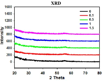
Fig.3-3 shows structure characterizations of a-IZTO thin film. In XRD patterns, a-IZTO thin film with different oxygen flow rate incorporation do not exhibit sharp diffraction peaks assignable to crystalline phase or poly phase. As a result, the thin films with different oxygen flow rate remain the amorphous phase after annealing process. Table 3-1 shows the film ele-mental composition by XPS analysis, it reveals that oxygen incorporation doesn’t have sig-nificant influence in elemental composition since the oxygen concentration in Table 3-1 has no obvious tendency.
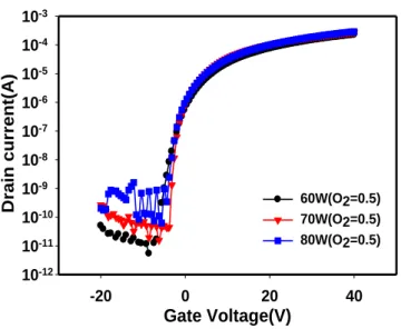
The transfer characteristics and other parameters of a-IZTO TFTs fabricated by three different RF sputter power with the same thickness 30nm and consistent oxygen flow rate (0.5 sccm) were shown in Fig.3-4 and Table 3-2. From the Table 3-1, TFT with power 70w has the relatively good characteristic, as a result, we choose the power 70w as our experiment RF sputtering power.
Fig.3-5 shows the relation between deposition rate (nm/min) and oxygen flow rate(sccm) with power 70w. The film thicknesses were measured by AFM system in order to get the dep-osition rate. From the figure, we found that depdep-osition rate is clearly deceases when the oxy-gen flow rate increases.
16
3.1.2 Characteristic analysis of a-IZTO TFTs with different oxygen flow rate
The a-IZTO TFTs using bottom gate staggered structure were fabricated with different oxygen flow rate and different thickness. The electrical performance shows in Fig.3-6(a), (b) and (c). Error bar in Fig.3-7 presents the overall characteristic of different oxygen flow rate with different thickness. The performance with different thickness has the same tendency for the mobility, threshold voltage, and sub-threshold swing. Mobility decreases as the oxygen flow rate increase. Threshold voltage increase as the oxygen flow rate increase, and sub-threshold swing increase when the oxygen flow rate increase as well. For the discussion of variation, devices with thickness 10nm have the lowest variation whether on mobility, threshold voltage, or sub-threshold swing. Also, devices with thickness 10nm have higher mobility and lower sub-threshold swing rather than the others.
When it comes to the same tendency of threshold voltage in three different thickness, from the literature, as the n-type oxide semiconductor, a well-known mechanism
for doping is that the oxygen vacancy generates two free electrons in the conductor band and works as a shallow donor. The higher quantity of oxygen incorporation may decrease the ox-ygen vacancy in the a-IZTO film.[15,16] In our experiment, we also found that threshold voltage increases when the oxygen flow rate increases. From this result, we can infer that due to the increasing oxygen flow rate, oxygen vacancy decrease which results in the increasing threshold voltage.
17
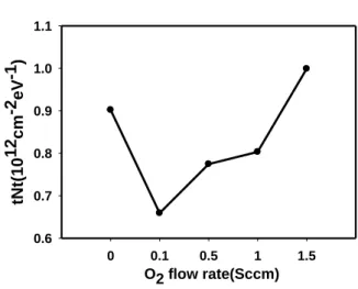
On the other hand, the trap densities of a-IZTO film (Nt) can be estimated from sub-threshold swing value with the following formula.[17,18]
S. S. = ln ×
𝑘𝑇 𝑒× [ +
𝑒(𝑡𝑁𝑡+𝐷𝑖𝑡) 𝐶𝑜𝑥]
(3-1) where k is Boltzmann constant T is temperature(K)t is the channel thickness(nm) Cox is the gate capacitance per area e is elementary electric charge Nt is the shallow trap density Dit is the interface trap density
Assuming the trap tNt dominated and Dit is negligible, we can calculate the Nt of different oxygen flow rate. From the Fig.3-8 and Table 3-3, take 10nm a-IZTO for example, we can find that trap states increase as oxygen flow rate increases. Moreover, we also discovered that when the oxygen flow rate increases from 0 sccm to 0.1 sccm, trap states apparently decrease. This result also indicates that the a-IZTO thin film requires proper quantity of oxygen to re-pair its defects and optimize the characteristic, but too much oxygen incorporation may con-trarily result in increasing defect.
18
3.1.3 Characteristic analysis of a-IZTO TFTs with different channel thickness
Fig.3-9(a) shows the transfer characteristic of a-IZTO TFTs with no oxygen
incorporation on three different channel thickness (10nm,30nm,50nm). From the figure, the device with no oxygen incorporation at 10nm shows the normal thin film transistor characteristic, however, the device with 30nm is more conductive than 10nm device with ex-tra negative threshold voltage and 50nm has even more conductive characteristic than the others. Through the result, we can infer that the quantity of carriers increase when the channel thickness increases. When it compares with the device deposited with 0.1 sccm oxygen flow rate as shown in Fig.3-9(b), the result reveals the oxygen incorporation suppresses the carrier concentration that even 50nm device has thin film transistor characteristic although the threshold voltage are getting negative as the channel thickness increases.
When the oxygen flow rate increases to 0.5 sccm, three different thickness(10nm,30nm,50nm) devices are all have similar characteristic, and then, we fabricated thicker a-IZTO devices (70nm,90nm,110nm) as shown in Fig.3-10. The result indicates that the oxygen flow rate 0.5 sccm is not enough to suppress the carrier concentration of thicker a-IZTO thin film.
3.1.4 Summary
19
is still in amorphous phase with different oxygen flow rate incorporation after 300oC anneal-ing process. The increasanneal-ing oxygen flow rate cause (1) the mobility decreases (μ↓), (2) the threshold voltage positively shifts (Vth↑), (3) sub-threshold swing increases (S.S ↓). On the
other hand, the trap density increases when oxygen flow rate increases.
3.2 Reliability Analysis of a-IZTO TFTs
3.2.1 Electrical reliability analysis under gate bias stress
As shown in Fig.3-7, the result shows that devices with thickness10nm have the lowest variation whether on mobility, threshold voltage, or sub-threshold swing. For the discussion of the effect on different oxygen flow rate, we uses the a-IZTO TFTs with thickness10nm to have reliability analysis in vacuum in order to isolate from ambiance influence.
Fig.3-11(a),(b) shows the threshold voltage (Vth) shift of a-IZTO TFT devices under
pos-itive gate bias stress (PGBS) and negative gate bias stress (NGBS) for the time duration of 2000 seconds, respectively. And Fig.3-12(a),(b) shows subthreshold swing (S.S.) shift of a-IZTO TFT devices under positive gate bias stress (PGBS) and negative gate bias stress (NGBS) for the time duration of 2000 seconds. The Vth shift of PGBS apparently increase
with oxygen flow rate increases except the oxygen flow rate 0.1 sccm is 1.5V, a little bit smaller than 0 sccm about 1.6V.
20
in subthreshold swing (S.S.) shift under positive gate bias stress (PGBS) and negative gate bias stress (NGBS) as shown in Fig.3-12. The phenomenon means the shift of Vth is not
ac-companied by the sub-threshold slope degradation, which indicates that the Vth shift in
a-IZTO is attributed to the trapping of electrons in the interface or bulk dielectric layers with negligible creation of additional interface traps[19,20]. The trapped electrons partially screen the applied electric field so that the effective applied gate voltage is smaller when trapped electrons exist at the interface or bulk dielectric layers. When negative gate bias stress is ap-plied to the gate electrode, the transfer curve hardly moves from the initial one, which is due to the depletion of carriers in the active layer. To better understand the mechanism in the process of the charge trapping and detrapping through bias stress, we found that our results show that the time dependence of the Vth is in agreement with the stretched exponential
equation, which has been developed to model Vth by the charge trapping mechanism in a-Si
TFTs. [21]
The stretched-exponential equation for the Vth is defined as :
| | = | | { [ ( ) ]} (3-2) Where
= G_S ress _ini ial (3-3)
and
τ= τ (Eτ
21
is effective stress voltage
_ini ial is the initial threshold voltage
τ is the characteristic trapping time of carriers β is the stretched exponential exponent
Eτ is the average effective energy barrier that electrons in the a-IZTO TFT channel need to overcome before they can enter the insulator. And τ is a significant parameter which can be inferred as the time duration of electron needed to be trapped or detrapped from the defect, which is mean, when the τ is increase, the carriers need more time to be trapped by defects as we can say the defects or trap states decrease, and vice versa. Fig.3-13 shows that the loga-rithmic time dependence of Vth can be well fitted with the stretched-exponential equation,
and the Table3-4 are the τ and correlative parameters. From Table3-4, device with oxygen flow rate 0.1 sccm has the largest τ, and it decease when oxygen flow rate increases. This re-sult is consistent with the previous experiment in trap state extraction, the τ of device with no oxygen incorporation is smaller than of 0.1 sccm. It confirms that defects increase when oxy-gen flow rate increases, but the proper quantity of oxyoxy-gen can repair defects and optimize the characteristic.
22 3.2.2 The photosensitivity analysis
As shown in Fig.3-14(a), the 30nm film with different oxygen flow rate transparent through the visible spectrum. All the film transmittance is great than 80% from 400nm to 700nm. And from Tauc model as mentioned in eq.(2-7), Fig.3-14 (b) shows the relationships between (αhν)2 and the photon energy (hν), the optical band-gaps, Eg, can be obtained by ex-trapolating from the linear region onto the axis of photon energy throught the fitting curve. And the Table3-5 shows the optical band-gaps for 30nm a-IZTO thin film with different oxy-gen flow rate extracted from Fig.3-14 (b). From the table, we observed that thin films do not have obvious difference approximately 3.7eV with different oxygen flow rate.
In order to study the instability under visible light illumination, for device different oxy-gen flow rate, the devices in 10nm a-IZTO expose in different wavelength illumination were investigated. Fig.3-15(a)~(e) show the corresponding transfer curves of devices with different oxygen flow rate, respectively, which are subjected to various colored visible light illumina-tion (380nm~700nm) without applying bias. From Fig.3-15(a)~(e), we can find that the de-vices with different oxygen flow rate are insensitivity to the visible light.
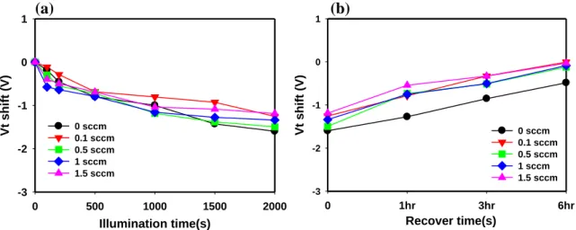
For the further investigation of instability of reality, we use the light source with full-band spectrum similar to flat panel back light illumination. Fig.3-16 shows the back light spectrum with intensity. Fig.3-17(a) shows the the threshold voltage (Vth) shift under light
23
at 1 hour, 3 hour, and 6 hour after the light illumination. From the figure, threshold voltage (Vth) of all devices shift negatively for small amount about 1.3V, and will recover for a period
of time. This result shows, the light generated electron hole pairs, causing more conductive on active layer. As in Fig.3-16, the wavelengh in blue light has the highest intensity in this full band spectrum, even so, the threshold voltage (Vth) shows a mall amount of shift on a-IZTO
TFT. It is clearly again to observe that the devices with different oxygen flow rate are insensi-tivity to the visible light.
Moreover, the negative bias illumination stress (NBIS) induced instability of the electrical properties was also investigated under the back light illumination. In the stress conduction, the gate voltage was fixed at the VG of -25V and the S/D electrodes were grounded. In
Fig.3-18(a), voltage shift dosen’t have obvious tendency in different oxygen flow rate. The voltage shifts for five oxygen flow rates are about -15V which is much bigger than negative gate bias stress without illumination. The light induced electron hole pairs from deep level state, and free hole carriers were attracted to the interface by negative bias, as a result, elec-trons in channel result in the negative voltage shift. As we know from literature, electron hole pairs generated from illumination are come from deep level state [26], and this also means that oxygen incorporation doesn’t have significant influence in deep level trap state since the voltage shifts are about -15V and with no obvious tendency. Again with stretch exponential fitting shown in Fig.3-18(b) and Table 3-6, τ has no obvious tendency as well.
24 3.2.3 Summary
Through stretched exponential equation analysis under positive gate bias stress, the fit-ting result shows that defects increase when oxygen flow rate increases. And shifts of thresh-old voltage do not have obvious change in negative bias stress. The devices show insensitivity to the visible light, only under the full band spectrum with the highest intensity in blue light, the threshold voltage shifts negatively for about 1.3V. In NBIS, voltage shift dosen’t have obvious tendency in different oxygen flow rate, that means, oxygen incorporation doesn’t have significant influence in deep level trap state.
3.3 Application of a-IZTO TFTs for ultra-thin glass panel
3.3.1 Introduction
Recently, there has been considerable interest in flexible displays, as they facilitate the fabrication of displays that are thin, lightweight, robust, conformable, and flexible. [22]Large-area electronics composed of thin-film transistors TFTs have been fabricated mainly on rigid glass substrates. The substrates and the housing bodies to protect the sub-strates from the damage occupy the greater part of the electronics in volume and determine their total weight.[23] The primary flexible substrate candidates are plastics and thin glass. Plastic substrates are inexpensive, roll-to roll processable and can be laminated to multi-layers, but they also impose limitations with respect to thermal processing and barrier performance.
25
Ultra-thin glass (0.13mm) substrates have recently caught attention because they exhibit bet-ter thermal stability, light weight, higher visual transparency than plastics and the bending potential.[24] For the advantages of ultra thin glasses, they can also apply in transparent mo-bile display, google glass, etc.
3.3.2 Device structure
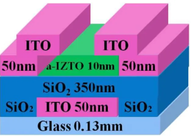
Fig.3-19 shows the structure of a-IZTO TFT fabricated on ultra thin glass (0.13mm).
Fabrication flows were the same with the ones fabricated on Si wafer as written in chapter 2, except the gate insulator was fabricated by PECVD with 350nm and gate electrode was an-nealed at 300℃ before the gate insulator deposited. 10nm a-IZTO TFTs with oxygen flow rate 0.1sccm fabricated on ultra thin glass were all have annealing process after the device fabrication. Fig.3-20 (a), (b) is the side view and top view of a-IZTO TFT fabricated on ultra thin glass.
3.3.3 Electrical characteristic analysis
Since the devices in 10nm have relatively nice characteristic, from the aspect of mobility, comparison of five different oxygen flow rate in mobility are shown in Table 3-7,the device with oxygen flow rate 0.1 sccm has the highest mobility. As a result, we choose this oxygen condition to transfer from Si wafer to ultra thin glass.
26
Fig3-21 shows the electrical performance of the device with oxygen flow rate 0.1 sccm. From the figure, it shows that the device fabricated on ultra thin glass still has good uniformi-ty, and a little decrease in mobility about 12~13cm2/V.s. Table 3-8 compares the relative pa-rameters for ultra thin glass and Si wafer.
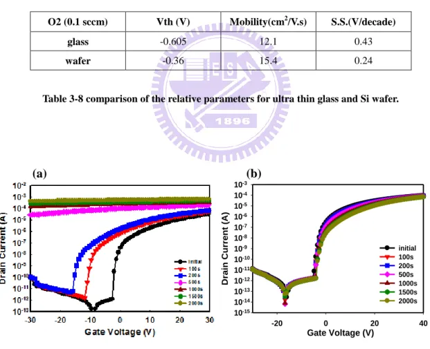
3.3.4 Electrical reliability analysis under gate bias stress
Fig.3-22 (a), (b) shows the electrical performence of a-IZTO TFT devices under posi-tive gate bias (25V) stress (PGBS) and negaposi-tive gate bias (-25V)stress (NGBS) for the time duration of 2000 seconds, respectively. We can clearly discover that the tendency of 𝑉𝑡ℎ shift is completely opposite to the tendency on Si wafer. In addition, a threshold voltage shift is easily observed as numbers of traps exist at the active layer/dielectric interface by for-ward/reverse voltage sweep. Therefore, the hysteresis measurement is usually performed to investigate the influence of charge trapping. [25] Fig.3-23 shows the hysteresis in transfer characteristics observed between forward (VG = -40Vto 40 V) and reverse (VG = 40 V to -40
V) gate voltage sweeps. Clearly, the threshold voltage shift ( ) is about -4 V. That is, from Fig.3-23 , the forward curve shows normal transistor characteristic, however in the reverse part, when positive gate bias(40V) continued sweep toward negative, this phnonmenon is similar to short period of positive gate bias stress. The threshold voltage shift negatively indi-cate that channel is easier to turn on. We guess that when gate electrode was treated by
posi-27
tive bias, free carriers with positive charging were depleted from gate electrode to gate insu-lator, catching more electrons on the interface of gate insulator and active layer, causing more conductive in TFT characteristic. And the negative gate bias stress can be explained in the same way as well. This phnonmenon is not consistent with the devices fabricated on Si wafesr, it reveals that the interface of gate electrode and gate insulator deposited by PECVD may need some of improvement.
3.3.5 Summary
10nm a-IZTO TFT device with oxygen floe rate 0.1 sccm was successfully transfered on
the ultra thin glass with stable, uniform basic characteristic and not bad mobility (12~13cm2/V.s.) . However, the gate bias stress has opposite tendency, through hysteresis measurement, it is regard as the poor interface of gate electrode and gate insulator deposited by PECVD.
28
(a) (b)
(c) (d) (e)
Fig.3- 1 The AFM results of 30nm IZTO film roughness for oxygen flow rate (a) 0 sccm, (b) 0.1 sccm, (c) 0.5 sccm, (d) 1 sccm, (e) 1.5 sccm, after annealing process
(a) (b)
(c)
(d)
(e)
Fig.3- 2 The SEM results of 30nm a-IZTO film surface for oxygen flow rate (a) 0 sccm, (b) 0.1 sccm, (c) 0.5 sccm, (d) 1 sccm, (e) 1.5 sccm, after annealing process
29
XRD
Fig.3- 3 XRD pattern of 30nm a-IZTO thin film for five different oxygen flow rate after annealing process
30 Gate Voltage(V) -20 0 20 40 Dr ai n cu rr en t( A) 10-12 10-11 10-10 10-9 10-8 10-7 10-6 10-5 10-4 10-3 60W(O2=0.5) 70W(O2=0.5) 80W(O2=0.5)
Oxygen Flow Rate(Sccm)
0 0.1 0.5 1 1.5 De po si ti on Ra te s (n m /m in) 1.5 2.0 2.5 3.0 3.5 4.0 4.5 deposition rate
Fig.3- 4 Transfer characteristics of three different RF sputter power with the same thickness 30nm and consistent oxygen flow rate (0.5 sccm)
Sputtering power(w) 60w 70w 80w
μ (cm2
/V.s) 11.0586 17.6081 14.4449
Vth (V) -3.71 -2.68 -3.31
S.S.(V/decade) 0.41 0.4 0.42
Table 3-2 Parameter of three different RF sputter power with the same thickness 30nm and consistent ox-ygen flow rate (0.5 sccm)
31 0 0.1 0.5 1 1.5 Mo b il it y (cm 2/V .s) 0 5 10 15 20 0 0.1 0.5 1 1.5 Vt h (V ) -12 -10 -8 -6 -4 -2 0 2 4 O2 flow rate(Sccm) 0 0.1 0.5 1 1.5 S. S( V/ d ecad e) 0.0 0.5 1.0 1.5 2.0 2.5 3.0 0 0.1 0.5 1 1.5 Mobi li ty (cm 2/V. s) 0 5 10 15 20 0 0.1 0.5 1 1.5 Vth(V) -12 -10 -8 -6 -4 -2 0 2 4 O2 flow rate(Sccm) 0 0.1 0.5 1 1.5 S.S(V/ decade) 0.0 0.5 1.0 1.5 2.0 2.5 3.0 0.1 0.5 1 1.5 Mob il ity (cm 2/V. s) 0 5 10 15 20 0.1 0.5 1 1.5 Vth(V) -12 -10 -8 -6 -4 -2 0 2 4 O2 flow rate(Sccm) 0.1 0.5 1 1.5 S.S(V/ decade) 0.0 0.5 1.0 1.5 2.0 2.5 3.0 Gate Voltage(V) -20 0 20 40 Drain Curr ent(A) 10-14 10-13 10-12 10-11 10-10 10-9 10-8 10-7 10-6 10-5 10-4 10-3 0 0.1 0.5 1 1.5 Gate Voltage(V) -20 0 20 40 Drain Curr ent(A) 10-13 10-12 10-11 10-10 10-9 10-8 10-7 10-6 10-5 10-4 10-3 10-2 0 0.1 0.5 1 1.5 Gate Voltage(V) -20 0 20 40 D ra in C u rr e n t(A ) 10-14 10-13 10-12 10-11 10-10 10-9 10-8 10-7 10-6 10-5 10-4 10-3 0 0.1 0.5 1 1.5 (a) (b) (c)
Fig.3-6 electrical performance with different oxygen flow rate in (a) 10nm (b) 30nm (c) 50nm.
(a) (b) (c)
32 Gate Voltage(V) -20 0 20 40 Drain Current(A) 10-13 10-12 10-11 10-10 10-9 10-8 10-7 10-6 10-5 10-4 10-3 10nm 30nm 50nm O2 flow rate(Sccm) 0 0.1 0.5 1 1.5 tNt( 10 12 cm -2 eV -1 ) 0.6 0.7 0.8 0.9 1.0 1.1 Gate Voltage(V) -20 0 20 40 Drain Current(A) 10-14 10-13 10-12 10-11 10-10 10-9 10-8 10-7 10-6 10-5 10-4 10-3 10-2 10nm 30nm 50nm
Fig.3-8 Relation between trap state and oxygen flow rate(sccm)
O2 (sccm) 0 0.1 0.5 1 1.5
Nt(cm-3eV-1) 9.02x10¹⁹ 6.59x10¹⁹ 7.75x10¹⁹ 8.03x10¹⁹ 9.99x10¹⁹
Table 3-3 Parameters of trap state of different oxygen flow rate with the thickness 10nm
(a) (b)
Fig.3-9 transfer characteristic of a-IZTO TFTs with oxygen flow rate (a) 0 sccm (b) 0.1 sccm in three different thickness.
33 Stress time(s) 0 100 200 500 1000 1500 2000 S.S. shi ft(V/ decade) -0.2 0.0 0.2 0.4 0.6 0.8 1.0 0_NGBS 0.1_NGBS 0.5_NGBS 1_NGBS 1.5_NGBS Stress time(s) 0 100 200 500 1000 1500 2000 S. S. shi ft (V/ dec ade ) -0.4 -0.2 0.0 0.2 0.4 0.6 0.8 1.0 0_PGBS 0.1_PGBS 0.5_PGBS 1_PGBS 1.5_PGBS Stress time(s) 0 100 200 500 1000 1500 2000 V t sh ift(V ) -3.0 -2.5 -2.0 -1.5 -1.0 -0.5 0.0 0_NGBS 0.1_NGBS 0.5_NGBS 1_NGBS 1.5_NGBS Gate Voltage(V) -20 0 20 40 Drain Current(A) 10-14 10-13 10-12 10-11 10-10 10-9 10-8 10-7 10-6 10-5 10-4 10-3 10-2 10nm 30nm 50nm 70nm 90nm 110nm Stress time(s) 0 100 200 500 1000 1500 2000 Vt sh ift (V ) 0 1 2 3 4 5 6 7 0_PGBS 0.1_PGBS 0.5_PGBS 1_PGBS 1.5_PGBS
Fig.3-10 transfer characteristic of the oxygen flow rate 0.5 sccm with different thickness.
(a) (b)
Fig.3-11 Threshold voltage (Vth) shift of 10nm a-IZTO TFT devices under (a) positive gate bias stress
(PGBS) and (b) negative gate bias stress (NGBS) for 2000 seconds.
(a) (b)
Fig.3-12 Subthreshold swing (S.S.) shift of 10nm a-IZTO TFT devices under (a) positive gate bias stress (PGBS) and (b) negative gate bias stress (NGBS) for 2000 seconds
34 Wavelength(nm) 300 400 500 600 700 800 900 Tra nsm itt anc e( % ) 40 50 60 70 80 90 100 0 0.1 0.5 1 1.5 Stress time(s) 101 102 103 Vt shi ft (V) 0 2 4 6 8 10 0_PBGS 0.1_PBGS 0.5_PBGS 1_PBGS 1.5_PBGS photo energy(eV) 1.5 2.0 2.5 3.0 3.5 4.0 4.5 h eV 2 cm -2 ] 0 5x10¹⁵ 10x1015 15x1015 20x1015
Fig.3-13 the logarithmic time dependence of Vth with the stretched-exponential fitting curve
O2 (sccm) 0 0.1 0.5 1 1.5
𝑽𝒕𝒉𝟎 25.06 25.48 24.9 24.19 24.09
𝛃 0.61 0.57 0.62 0.53 0.54
𝛕(s) 1.64x10⁵ 1.17x10⁵ 4.3x10⁴ 3.48x10⁴ 1.79x10⁴
Table3-4 Correlative parameters of stretched-exponential fitting curve
(a) (b)
Fig.3-14 (a) the 30nm film transmittance with different oxygen flow rate transparent through the visible spectrum. (b) the relationships between (αhν)2 and the photon energy (h ν)
35 1.5 Gate Voltage(V) -40 -20 0 20 40 Dra in Cu rr ent (A) 10-13 10-12 10-11 10-10 10-9 10-8 10-7 10-6 10-5 10-4 10-3 dark 700nm 600nm 500nm 400nm 380nm recovery 1 Gate Voltage(V) -40 -20 0 20 40 D rain Cu rrent(A ) 10-13 10-12 10-11 10-10 10-9 10-8 10-7 10-6 10-5 10-4 10-3 dark 700nm 600nm 500nm 400nm 380nm recovery 0.5 Gate Voltage(V) -40 -20 0 20 40 Drain Current(A) 10-13 10-12 10-11 10-10 10-9 10-8 10-7 10-6 10-5 10-4 10-3 dark 700nm 600nm 500nm 400nm 380nm recovery 0.1 Gate Voltage(V) -40 -20 0 20 40 Drain Cu rrent(A) 10-12 10-11 10-10 10-9 10-8 10-7 10-6 10-5 10-4 10-3 dark 700nm 600nm 500nm 400nm 380nm recovery 0 Gate Voltage(V) -40 -20 0 20 40 D rain Cu rre nt(A ) 10-13 10-12 10-11 10-10 10-9 10-8 10-7 10-6 10-5 10-4 10-3 dark 700nm 600nm 500nm 400nm 380nm recovery
Table3-5 optical band-gaps for 30nm a-IZTO thin film with different oxygen flow rate
(a) (b)
(c) (d) (e)
Fig.3-15 Transfer curves of devices with oxygen flow rate (a) 0 sccm, (b) 0.1 sccm, (c) 0.5 sccm, (d) 1 sccm, (e) 1.5 sccm under visible light illumination
Fig.3-16 back light spectrum with intensity.
O2 (sccm)
0
0.1
0.5
1
1.5
36 Recover time(s) 0 1hr 3hr 6hr Vt shi ft (V) -3 -2 -1 0 1 0 sccm 0.1 sccm 0.5 sccm 1 sccm 1.5 sccm Illumination time(s) 0 500 1000 1500 2000 Vt shi ft ( V) -3 -2 -1 0 1 0 sccm 0.1 sccm 0.5 sccm 1 sccm 1.5 sccm NBIS Stress time(s) 0 500 1000 1500 2000 Vt s hi ft ( V) -20 -18 -16 -14 -12 -10 -8 -6 -4 -2 0 O2= 0 sccm O2= 0.1 sccm O2= 0.5 sccm O2= 1 sccm O2= 1.5 sccm Stretch-exponential fitting Stress time(s) 101 102 103 104 Vt s hi ft (V ) -30 -25 -20 -15 -10 -5 0 0_NBIS 0.1_NBIS 0.5_NBIS 1_NBIS 1.5_NBIS (a) (b)
Fig.3-17 Threshold voltage (Vth) shift of (a) light illumination for 2000 seconds without applying bias (b)
recovery mesurement at 1 hour, 3 hour, and 6 hour after the light illumination.
(a) (b)
Fig.3-18 (a) Threshold voltage (Vth) shift of light illumination for 2000 seconds with gate bias -25V (b) the
logarithmic time dependence of Vth with the stretched-exponential fitting curve
0 0.1 0.5 1 1.5
𝐕
𝐭𝐡𝟎(𝐕)
-25 -24.6 -25.1 -25.12 -25.35𝛃
1.04 1.16 1.14 1.12 1.15𝛕(𝐬)
2.35x10³ 1.88x10³ 1.96x10³ 1.82x10³ 1.85x10337
Flexible thin glass
Fig.3-19 Structure of a-IZTO TFT fabricated on ultra thin glass
(a) (b)
Fig.3-20 The (a) side view and (b) top view of a-IZTO TFT fabricated on ultra thin glass.
O2 flow rate(sccm) 0 0.1 0.5 1 1.5
Mobility(cm2/V.s) 10.49 15.4 12.93 10.76 9.85
38 Gate Voltage (V) -20 0 20 40 Drain Current ( A) 10-15 10-14 10-13 10-12 10-11 10-10 10-9 10-8 10-7 10-6 10-5 10-4 10-3 initial 100s 200s 500s 1000s 1500s 2000s
Fig 3-21 Electrical performance of the device with oxygen flow rate 0.1 sccm.
O2 (0.1 sccm) Vth (V) Mobility(cm2/V.s) S.S.(V/decade) glass -0.605 12.1 0.43
wafer -0.36 15.4 0.24
Table 3-8 comparison of the relative parameters for ultra thin glass and Si wafer.
(a) (b)
Fig.3-22 Electrical performence of a-IZTO TFT devices under (a) positive gate bias (25V) stress (PGBS) and (b) negative gate bias (-25V)stress (NGBS) for the time duration of 2000 seconds
Gate Voltage(V) -20 0 20 40 Dra in Curr ent(A ) 10-15 10-14 10-13 10-12 10-11 10-10 10-9 10-8 10-7 10-6 10-5 10-4 10-3 200/400L 200/400R 200/600R 400/600L 400/600R
39
Gate Voltage (V)
-60 -40 -20 0 20 40 60
Drain Current (A)
10-14 10-13 10-12 10-11 10-10 10-9 10-8 10-7 10-6 10-5 10-4 10-3 Forward Reverse
Fig.3-23 Hysteresis in transfer characteristics observed between forward (VG = -40Vto 40 V) and reverse (VG = 40 V to -40 V) gate voltage sweeps.
40
Chapter 4
Conclusion
_______________________________________________________________________
4.1 Conclusions
In this study, a-IZTO TFT was investigated with its (a) rare element (Ga) displacement, (b)High mobility, (c) relative low annealing temperature, and we obtained the optimized characteristic which is 10nm a-IZTO with oxygen flow rate 0.1 sccm. And the optimized mo-bility can reach 15~17cm2/V.s.
From the trap state extraction and stretch-exponential fitting in PGBS , 10nm a-IZTO TFT with oxygen flow rate 0.1 sccm has the best reliability due to the less bulk trap density, and the defects concentration increase in a-IZTO thin film when the oxygen flow rate in-creases. In NBIS, Vth shifts don’t have obvious difference in all oxygen flow rates, that is, oxygen incorporation does not have significant influence on deep level trap state. For the fu-ture application, optimized characteristic of a-IZTO TFT was successfully fabricated on ul-tra-thin glass. With its good uniformity, transparency and comparable mobility with it on Si wafers, this application shows potential in the future.
41
4.2 Future work
Base on the result of opposite tendency under the gate bias stress on ultra thin glass, the interface of gate electrode and gate insulator need to be improved. Changing the gate material is one of the possible ways to improve the interface quality. The a-IZTO TFTs with large channel thickness can be discussed in order to futher understand characteristic of thicker channel a-IZTO TFTs in reliability and photosensitivity.
42
Reference
_______________________________________________________________________ [1] K. Nomura, H. Ohta, A. Takagi, T. Kamleya, M. Hirano, H. Hosono, Nature 432 (2004). [2]K. H. Lee, J. S. Jung, K. S. Son, J. S. Park, T. S. Kim, R. Choi, J. K. Jeong, J. Y. Kwon, B. Koo, and S. Lee, Appl. Phys. Lett 95, 232106 (2009)
[3] T. Kamiya, K. Nomura, and H. Hosono, Sci. Technol. Adv. Mater. 11 (2010) 044305 [4] T. Kamiya, Z. A. K. Durrani, and H. Ahmed, J. Vac. Sci. Technol. B 21, 1000 (2003) [5] Joseph W. Tringe, and James D. Plummer, J. Appl. Phys. 87, 7913 (2000)
[6] T. Kamiya, K. Nomura, and H. Hosono, J. Dis. Tech, vol. 5, no. 12, (2009)
[7] E. M. C. Fortunato, P. M. C. Barquinha, Ana C. M. B. G. Pimentel, A. M. F. Gonçalves, A. J. S. Marques, Appl. Phys. Lett. 85, 2541 (2004)
Rodrigo F. P. Martins, and Luis M.N. Pereira
[8] H. S. Bae and S. Im, J. Vac. Sci. Technol. B 22, 1191 (2004)
[9] R. L. Hoffman, B. J. Norris and J. F. Wage, Appl. Phys. Lett. 82, 733 (2003)
[10] E. M. C. Fortunato, P. M. c. Barquinha, C. M. G. Pimentel, A. M. F. Goncalve, A. J. S. Marques, L. M. N. Pereira, R. F. P. Martins, Adv. Mater, 2005, 17, NO.5
[11] S. P. Harvey, T. O. Mason, D. B. Buchholz, and R. P. H. Chang, J. Am. Ceram. Soc., 91 [2] 467–472 (2008)
43
[13] D. Wang, C. Li and M. Furuta, AM-FPD '12 [14] E.A. Davis, N.F. Mott, P. Mag. 22, 903 (1970)
[15] J. Yao, N. Xu, S. Deng, J. Chen, J. She, H..P. Shieh, Fellow, IEEE, P. T. Liu, Senior
Member, IEEE, and Y. P. Huang, ieee Tr. Elec. Dev, vol. 58, no. 4, april 2011
[16] K. H. Ji, J. I. Kim, H. Y. Jung, S. Y. Park, R. Choi, U. K. Kim, C. S. Hwang, D. Lee, H. Hwang, and J. K. Jeong1, Appl. Phys. Lett, 98, 103509 (2011)
[17] L. Shao, K. Nomura, T. Kamiya, and H. Hosonoa, Elec. S.State Lett, 14 (5) H197-H200 (2011)
[18] L. F. Teng, P. T. Liu, Y. J. Lo, and Y. J. Lee, Appl. Phys. Lett, 101, 132901 (2012) [19] I. T. Cho, J. M. Lee, J. H. Lee, and H. I. Kwon, Semicond. Sci. Technol. 24 (2009) [20] K. Nomura, T. Kamiya, M. Hirano, and H. Hosono, Appl. Phys. Lett. 95, 013502 (2009) [21] J. M. Lee, I. T. Cho, J. H. Lee, and H. I. Kwon, Appl. Phys. Lett. 93, 093504 (2008) [22] J. H. Jin , J. H. Ko , S. C. Yang , and B. S. Bae, Adv. Mater. 2010, 22
[23] H. Kumomi, K. Nomura, T. Kamiya, H. Hosono, Thin Solid Films 516 (2008) [24] S. Xi, Term Paper, Flexible Flat Panel Display
[25] S.W. Tsao, T.C. Chang, S.Y. Huang, M. C. Chen, S. C. Chen, C. T. Tsai, Y. J. Kuo, Y. C. Chen, W. C. Wub, Solid-State Electronics 54 (2010)
[26] H. Oh, S. M. Yoon, M. K. Ryu, C. S. Hwang, S. h. Yang, S. H. Park, Appl. Phys. Lett. 97, 183502 (2010)
44
[27] Y. D. Ko, C. H. Lee, D. K. Moon, Y. S. Kim, Thin Solid Films (2013), doi: 10.1016/j.tsf.2013.05.069