Thermal Stress Analysis for Rapid Thermal Processor
Ching-Kong Chao, Shih-Yu Hung, and Cheng-Ching Yu
Abstract—Within the framework of linearized thermoelasticity theory, the temperature and thermal stresses on the wafer for the rapid thermal processor are solved by using the finite-difference approach and a trapezoidal integration technique, respectively. Al-though the equations governing the present thermoelastic system are coupled in nature, the temperature can still be obtained inde-pendently due to the fact that the coupling term is negligible as a result of the strain rate being extremely small as compared with unity. Based on the maximum shear stress failure criterion, the calculated results show that material failure always occurs at the edge of the wafer at the beginning of cooling processes. Further-more, the maximum stress control scheme is proved to be more efficient that it can significantly reduce the required cooling time and thermal budgets. Thus, the conventional constant cooling-rate control scheme or linear temperature ramp-down scheme is not appropriate for the rapid thermal processor.
Index Terms—Cooling control, rapid thermal processor, thermal stress, transient heat transfer.
I. INTRODUCTION
T
HE CONTINUING miniaturization of IC components and the increasing function and performance of a single IC chip are the recent trends in the semiconductor industry. The quality control of the wafer is becoming more and more im-portant as the wafer becomes larger and the feature size shrinks. Rapid thermal processing (RTP) is used for various single-wafer thermal treatment processes including annealing, cleaning, ox-idation, and chemical vapor deposition. Because wafers pro-cessed using RTP have the advantage of fast ramp-up and -down time compared to conventional batch furnaces, it permits pro-cesses to be accomplished with minimal dopant redistribution and uniform deposition quality by the smaller thermal budget. However, poor RTP system design can lead to significant tem-perature difference in the wafer. One of the main shortcom-ings that RTP must overcome is that of heating (or cooling) the wafers ununiformly which would result in material failure due to increasing of thermal stresses or serious warpage. The damage due to the presence of thermal stresses can represent a limit to the applicability of the rapid thermal processing.The temperature nonuniformity in the wafer is caused by three factors: edge effect, pattern effect, and heat source. In this analysis, we consider only the edge effect. The higher heat loss from the wafer edge was found to result in a radial tem-perature gradient in the wafer. Hu [1] found that the tempera-Manuscript received February 24, 2001; revised November 20, 2002. This work was supported by the National Science Council, Republic of China, under Grant NSC 91-2212-E-011-032.
C.-K. Chao and S.-Y. Hung are with the Department of Mechanical Engi-neering, National Taiwan University of Science and Technology, Taipei 106, Taiwan, R.O.C. (e-mail: mailto:[email protected]).
C.-C. Yu is with the Department of Chemical Engineering, National Taiwan University, Taipei, Taiwan 106-17, R.O.C.
Digital Object Identifier 10.1109/TSM.2003.811884
ture gradient induces a thermal stress which is compressive in the central region of the wafer but is tensile toward the edge of the wafer and can often exceed the yield stress in silicon wafers, causing plastic deformation. To improve the wafer tem-perature nonuniformity produced by the edge effect, several ra-diative shields were placed at the edge of the wafer to reduce the heat loss from the wafer edge and reflect the radiative en-ergy back into the wafer during the cooling process [2]. By varying the angle of the shield, an optimal shield configura-tion can be found to minimize the induced thermal stress [3]. However, this pattern would overheat the wafer edges during heating processes leading to a high stress level [4]. Hebb and Jensen [5] showed that pattern-induced temperature nonunifor-mity can cause plastic deformation during an RTP cycle and the problem is exacerbated by single-side heating, increased pro-cessing temperature, and ramp rate. Bentini et al. [6] found the strip heater induces much lower thermal stresses than the irra-diation of a free wafer. Furthermore, Perkins et al. [7] used a nodal analysis to discuss the thermal uniformity and stress min-imization during the steady state and transient phase of RTP. Jan and Lin [8] studied lamp configuration design for RTP sys-tems to achieve the necessary temperature uniformity. Lin and Chu [9] presented a systematic inverse-modeling analysis, com-pared to the purely trial-and-error approach, to determine the in-cident heat flux over a silicon wafer intuitively to ensure thermal uniformity during processing of the ramp-up and steady phase of RTP. Huang et al. [10] obtained the optimal arrangement of lamp rings and measurement locations on the wafer for the con-trol of rapid thermal processor. Their results show that a 42% improvement in temperature uniformity can be achieved using the proposed design procedure.
The temperature nonuniformity and discontinuous manufac-ture procedure (compared with batch furnace) are two limits to the applicability of the rapid thermal processing. In this work, we aim to provide reliable physical and mathematical models to obtain the temperature distribution and thermal stresses throughout the wafer under rapid thermal processing. The objective of this work is to find the optimum cooling control method in the cooling process, which ensures that material failure does not take place and the required cooling time is minimal.
II. THEORETICALANALYSIS
The physical model of the present study is shown in Fig. 1. The wafer is enclosed in a cylinderical chamber, where the oven is axis-symmetric in geometry and the governing equations are then developed in a cylinderical coordinate system. The wafer thickness is assumed to be thin enough as compared to the radius of the wafer , so we can regard this work as a one-dimensional plane-stress problem, that is, both the temperature and radial 0894-6507/03$17.00 © 2003 IEEE
Fig. 1. Physical model of RTP.
displacement are dependent of only. The partial differential equations of the present thermoelastic problem can be written as [11]
(1) (2) where , , and are density, specific heat, and thermal con-ductivity of silicon, respectively. denotes the reference tem-perature, the linear thermal expansion coefficient, Poisson’s ratio and Young’s modulus. and represent the ra-diative and convective heat flux leaving a wafer surface per unit wafer thickness, respectively.
Since the dilatational strain rate in (1) and the temperature gradient in (2) are responsible for the present coupled thermoelastic system, the solutions and must proceed simultaneously. The complexity of the coupled thermoelastic problem makes an analytical solution difficult and often beyond reach. In order to make the solution accessible, we first examine the order of the coupling term
compared with other terms. In the present work, the material physical properties of the silicon wafer are given in Table I and the reference temperature is fixed at
C. Table I shows the material physical properties are weakly dependent on temperature between 600 C and 1200 C, which can be regarded as temperature-independence constants except for the thermal conductivity and specific heat. For this reason, the material physical properties are taken as the average values but the thermal conductivity and specific heat are consid-ered using the reported data [9].
At the beginning of cooling processes, the radiation term can be approximately estimated by , where is the Stefan–Boltzmann constant, the temperature of the wafer on the steady-state C, and the room
tempera-ture C. The strain-rate is still only
about 10 s even though the lamp’s power decreases instan-taneously to zero, i.e., power off. This amounts to the value of
coupling term being the order
of 2 10 , which is far less than the value of order 2 10 for the radiation term . It therefore allows us to discard the cou-pling term from (1) such that the energy equation for the present
TABLE I
MATERIALPHYSICALPROPERTIES OFSILICONWAFER
transient heat transfer problem becomes uncoupled and the tem-perature can be solved independently from (1).
A. Temperature Analysis
With the absence of the coupling term
, the governing equation (see (1)) of the present transient heat transfer problem can thus be written as
(3) with boundary conditions given by
at (4)
at (5)
where the quantity is the heat flux at the wafer edge that includes the heat loss of convection and radiation.
Since no analytical solution is available for the present problem, a numerical solution is sought to this set of equations. The approach used is to divide the wafer and oven into and concentric annular elements, respectively. Within each annular element, the wafer temperature or lamp power is assumed to be uniform. In the present study, the lamps are assumed to be a flat black body radiation source, the sidewall is assumed to be adiabatic, and the wafer is assumed to be gray and diffusive. Radiation energy interchange between the oven and the wafer can be evaluated by the following network theory [12]:
(6)
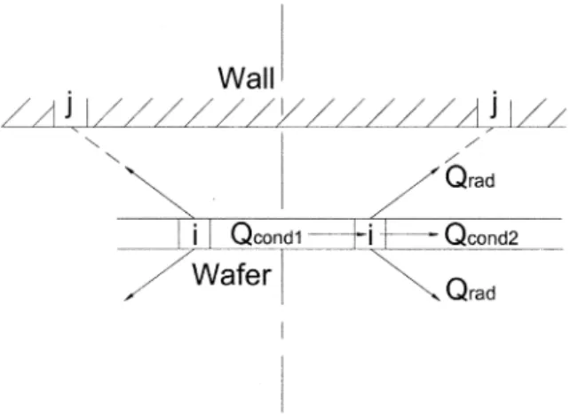
where and are the view factor from the wafer element to the oven element and the wafer emissivity, respectively, while and represent the blackbody emissive power of the wafer element and the oven element , respectively (Fig. 2). The wafer is 200 mm (about 8 in) in diameter held by three quartz pins and 24 mm above the bottom of a rapid thermal processing oven that is 560 mm in diameter and 100 mm in height. The convective heat transfer coefficient can be eval-uated from an equation experimented by Lord [2]
W/m C (7)
Fig. 2. Schematic representation of energy flux in an Si wafer.
where denotes the normalized radius and stands for the convective heat transfer coefficient at the edge of the wafer. The convective effect can be represented as
(9) with being the temperature of the reaction vapor.
We now consider the lamps blackbody emissive power on the steady state. The lamp’s power of the oven and the tem-perature distribution on the wafer are assumed to be uniform, thus the steady-state lamps blackbody emissive power can be written in the form
(10)
where is the steady-state wafer blackbody emissive power, is the surface area of wafer, and the is the global view factor from the wafer to the lamps which is found to be 0.925 in this work.
The numerical solution is carried out by using a fully implicit algorithm and computed by marching forward from the initial condition
for all on the wafer at (11)
The consistency and convergence of the present numerical solu-tion can be achieved by refining the mesh and time step. Since the nonlinear equations represented above are solved by a linear algorithm, the whole process needs a series of iterations. The convergence of the iterations is defined by
(12)
where the subscript stands for the number of iterations.
B. Stress Analysis
Once the temperature has been obtained, the displacement can be solved directly from (2). In the present study, the changes of thermal condition are assumed to proceed slowly such that
the inertia term in (2) can be discarded [10]. With this assumption, the displacement can be readily found as
(13) and the components of stresses are obtained as
(14)
(15) (16) where and are the radial and tangential stress compo-nents, respectively. Since the obtained temperature is expressed in a discrete manner, both the displacement in (13) and the stresses in (14) and (15) are determined by a trapezoidal inte-gration technique.
In the present study, the maximum shear stress failure crite-rion is used which assumes that the wafer fails in shear when
(17) where is the normalized maximum resolved stress, is the safety factor which is usually taken to be two, and the maximum shear stress is calculated using Mohr’s circle as [13]
(18) At high temperatures, silicon behaves like a viscous material, the yield stress in shear can be expressed in terms of the tem-perature and the maximum shear stress rate [2], [5], [14] as
(19) where the stress unit is in Pascal and the temperature unit is in degrees Celsius. The stress rate is taken to be the larger of 2.5 10 Pa/s or its calculated value. If the result calculated from (19) exceeds 3.1 10 Pa, it is taken to be 3.1 10 Pa which means that the wafer is at a low temperature. From (19), we know that the yield shear stress will be about 1.5 MPa when C at the beginning of the cooling process which is far less than 310 Mpa at the room temperature C. This simply indicates that, according to the failure criterion stated in (17), a small temperature nonuniformity may induce material failure at a high temperature.
III. RESULTS ANDDISCUSSION
Numerical solutions of (3) and (14) and (15) were obtained using a fully implicit finite-difference method and a trapezoidal integration technique, respectively. We first consider the heat transfer effects of convection and radiation to the wafer. From Fig. 3, curve (a) represents the radiative-only cooling with the
Fig. 3. Convective heat loss is small and negligible compared with radiative heat loss especially at a high temperature.
top and bottom of the oven, which are maintained at room tem-perature (27 C) while the oven is assumed to be vacuum. Curve (b) represents the convective-only cooling with reaction vapor, which is kept at 27 C while the top and bottom of the oven are assumed to be adiabatic. At the beginning of cooling processes, we can estimate from (7) and (9), which is about the order of 2 10 . That is much less than the value of order 2 10 for the radiation term . By that reason, the thermal energy of the radiation is proportional to absolute temperature to the fourth power, and the convective heat loss is believed to be small and negligible compared with the radiative heat loss especially at high temperature [2]. Furthermore, the radiative heat loss is found to be highly uniform over the time as compared to the convective heat loss as shown in Fig. 4. Based on the above find-ings, the convective heat loss may be a major factor in causing temperature variation across the wafer. The phenomenon fur-ther suggests that the convective cooling is not a good choice at the beginning of the cooling process, thus the following discus-sion will not consider the convective effect during the cooling process.
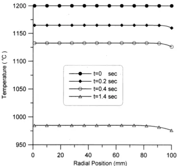
Fig. 5 shows the temperature profile during ramp-down for the radiative-only cooling process. Since the area of heat loss is larger at the edge of the wafer, the temperature drop is expected at the edge of the wafer. On the contrary, the temperature profile at the central region of the wafer is seen to be flatter.
Fig. 6 shows, for the radiative-only cooling process, the tangential stress at the wafer edge is positive due to thermal shrinkage induced by the edge effect. On the other hand, the compressive tangential stress prevails at the central region of wafer. From curve (a) in Fig. 4 and curve (c) in Fig. 6, it is interesting to see that the maximum temperature nonuniformity and the maximum tangential stress occur at the same time
s .
In this work, we consider three different boundary conditions of the oven during the cooling process: 1) the top and bottom of the oven are kept at room temperature (27 C); 2) the lamp
Fig. 4. Radiative heat loss is highly uniform compared with the convective heat loss.
Fig. 5. Temperature profile on the wafer for the room temperature (top and bottom of the oven) cooling condition.
power on the top of the oven decreases gradually and the bottom of the oven is a cold floor maintained at 27 C; 3) the lamp power on the top and bottom of the oven decrease gradually under a constant cooling-rate control scheme (10 kW/m s). According to the maximum shear stress criterion stated in (17), material failure is found to take place in cases (a) and (b) at the beginning of cooling processes, whereas the normalized max-imum resolved stress is always below one during the cooling process for the case (c) with the constant cooling-rate condition as indicated in Fig. 7. Note the time s at which the max-imum resolved stress takes place, as shown in Fig. 7, which is different from that of s where the maximum tangen-tial stress occurs, as shown in Fig. 4, for the room temperature
Fig. 6. Tangential stress distribution on wafer for the room temperature (top and bottom of the oven) cooling condition.
Fig. 7. Variation of the normalized maximum resolved stress at the wafer edge under three different boundary conditions.
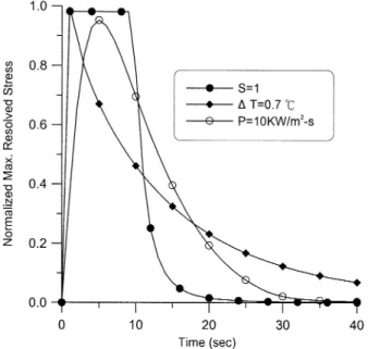
cooling condition. The reason is the yield stress in shear at s is greater than at s as indicated in (19). Next, we consider three different control schemes in the cooling process using the boundary condition that the lamps power on the top and bottom of the oven decrease with various cooling-rate conditions: 1) fixed temperature-difference control scheme—the maximum temperature difference within a wafer maintains constant which is determined to be 0.7 C by trial and error such that the normalized maximum resolved stress is less than one during the cooling process; 2) constant cooling-rate control scheme—the lamp’s power decreases gradually at a constant rate which is determined to be 10 kW/m s by
Fig. 8. Variation of the temperature difference during cooling process under three different control schemes.
Fig. 9. Variation of the normalized maximum resolved stress at the wafer edge under three different control schemes.
trial and error, which ensures that the normalized maximum resolved stress is less than one during the cooling process; and 3) maximum stress control scheme—the normalized maximum resolved stress is kept close to one until the lamp’s power decreases to zero during the cooling process.
Fig. 8 shows the temperature nonuniformity under three dif-ferent control schemes. It is seen that, initially, the allowable temperature difference is getting larger as time increases until the peaks s and s for the maximum stress control and constant cooling-rate control, respectively. This is because the lamp’s power reaches zero at s and s for the maximum stress control and constant cooling rate control, respectively, as shown in Fig. 10.
Fig. 10. Variation of the lamp’s power under three different control schemes.
Fig. 9 shows the corresponding normalized maximum resolved stress for three different control schemes. The normal-ized maximum resolved stress remains at unity until s for the maximum stress control scheme. After s, the lamp’s power is down to zero and thus the normalized resolved stress decreases accordingly (Fig. 10) as the result of decreases of the temperature at the wafer edge (e.g., from 900 C to 600 C as shown in Fig. 11). It is then suggested that after s the wafer can be cooled by other more efficient ways, for example convective cooling. Under the constant cooling-rate and fixed temperature-difference control schemes, the normalized maximum resolved stresses reach their the maximum value at s and s, respectively, and then the normalized maximum resolved stresses decrease subsequently.
Fig. 10 shows the lamps power decreases dramatically during the first 2 s for both the maximum stress control scheme and the fixed temperature-difference control scheme. After 5 s elapsed, the lamp’s power for the fixed temperature-difference control scheme decreases gradually with the rate even smaller than the constant cooling-rate control scheme. This is because the temperature nonuniformity C for the fixed temperature-difference control scheme is smallest among the three different control schemes as indicated in Fig. 8. The required cooling time for the maximum stress control scheme is only 18 s from 1200 C to 600 C, compared to 30 s for the constant cooling-rate control scheme, and, moreover, it is only one-fifth of the required time for the constant tempera-ture-difference scheme as shown in Fig. 11. From the above discussion, we conclude that the maximum stress control scheme can significantly reduce the required cooling time and thermal budgets compared with other ways. Moreover, this can be achieved by programming the lamp power (e.g., Fig. 10) or setting the temperature according to Fig. 11 for closed-loop control. The results further indicate the inappropriateness of the current linear temperature ramp-down practice.
Fig. 11. The temperature variation at wafer edge under three different control schemes.
IV. CONCLUSION
The temperature and the induced thermal stresses during the cooling process are calculated by the finite-difference method and a trapezoidal integration technique, respectively. It is shown that material failure initiates in the peripheral region of the wafer and the convective effect is a major factor to cause tempera-ture nonuniformity. Therefore, the convective cooling is not a good cooling mechanism in the initial stage during the cooling process. As for the radiative cooling, the temperature nonuni-formity is caused by edge effect and geometric relation between the chamber and the wafer. Among the three different boundary conditions, the two sides’ (top and bottom) room temperature radiative cooling condition is found to be the worst choice that the maximum takes place at s which would result in material failure. On the other hand, the two-side lamp’s radia-tive cooling condition is found to be the best choice because the
value is always below one during the cooling process. In this paper, we compare three control schemes using the lamp’s radiative cooling condition. Both the maximum allowed temperature nonuniformity and the maximum stress are predicted. The maximum stress control scheme is found to reduce the required cooling time at most compared with other ways, which promotes reliability and practicability of the rapid thermal processing. This phenomenon is consistent with the result associated with a batch furnace [15]. In this control scheme, the cleaning gas is suggested to flow through the chamber as the lamp’s power is down to zero (after 10 s). At this time, the wafer is strong enough to resist the thermal stress due to convection since the temperature is already down to about 900 C at which the yield stress in shear is increased accordingly, as indicated in (19).
REFERENCES
[1] S. M. Hu, “Temperature distribution and stresses in circular wafers in a row during radiative cooling,” J. Appl. Phys, vol. 40, no. 11, pp. 4413–4423, 1969.
[2] H. A. Lord, “Thermal and stress analysis of semiconductor wafers in a rapid thermal processing oven,” IEEE Trans. Semiconduct. Manufact., vol. 1, pp. 105–114, Sept. 1988.
[3] G. L. Young and K. A. McDonald, “Effect of radiation shield angle on temperature and stress profiles during rapid thermal annealing,” IEEE
Trans. Semiconduct. Manufact., vol. 3, pp. 176–182, Dec. 1990.
[4] S. A. Campbell and K. L. Knutson, “Transient effects in rapid thermal processing,” IEEE Trans. Semiconduct. Manufact., vol. 5, pp. 302–307, Dec. 1992.
[5] J. P. Hebb and K. F. Jensen, “The effect of patterns on thermal stress during rapid thermal processing of silicon wafers,” IEEE Trans.
Semi-conduct. Manufact., vol. 11, pp. 99–107, Mar. 1998.
[6] G. Bentini, L. Correra, and C. Donolato, “Defects introduced in silicon wafers during rapid isothermal annealing: Thermoelastic and thermo-plastic effects,” J. Appl. Phys., vol. 56, no. 10, pp. 2922–2929, 1984. [7] R. H. Perkins, T. J. Riley, and R. S. Gyurcsik, “Thermal uniformity and
stress minimization during rapid thermal processes,” IEEE Trans.
Semi-conduct. Manufact., vol. 8, pp. 272–279, Sept. 1995.
[8] Y. K. Jan and C. A. Lin, “Lamp configuration design for rapid thermal processing systems,” IEEE Trans. Semiconduct. Manufact., vol. 11, pp. 75–84, Mar. 1998.
[9] S. Lin and H. S. Chu, “Thermal uniformity of 12-in silicon wafer during rapid thermal processing by inverse heat transfer method,” IEEE Trans.
Semiconduct. Manufact., vol. 13, pp. 448–456, Dec. 2000.
[10] C. J. Huang, C. C. Yu, and S. H. Shen, “Selection of measurement loca-tion for the control of rapid thermal processor,” Automatica, vol. 36, no. 5, pp. 705–715, 2000.
[11] J. L. Nowinski, Theory of Thermoelasticity With Application. Alphen aan den Rijn, The Netherlands: Sijthoff & Noordhoff, 1978.
[12] F. P. Incropera and D. P. Dewitt, Fundamentals of Heat and Mass
Transfer. New York: Wiley, 1981.
[13] H. Reismann and P. S. Pawlik, Elasticity. New York: Wiley, 1980. [14] B. A. Boley and J. H. Weiner, Theory of Thermal Stresses. New York:
Wiley, 1960.
[15] Y. H. Fan and T. Qiu, “Analyzes of thermal stresses and control schemes for fast temperature ramps of batch furnaces,” IEEE Trans. Semiconduct.
Manufact., vol. 10, pp. 433–437, Dec. 1997.
[16] N. Miyazaki, H. Uchida, T. Munakata, and K. Fujioka, “Thermal stress analysis of silicon bulk single crystal during Czochralski growth,” J.
Crystal Growth, vol. 125, pp. 102–111, 1992.
Ching-Kong Chao received the B.S. and M.S.
degrees in mechanical engineering from National Cheng Kung University, Tainan, Taiwan, R.O.C., and National Taiwan University, Taipei, Taiwan, R.O.C., respectively, and the Ph.D. Degree in mechanical engineering from Lehigh University, Easton, PA, in 1987.
His current research interests include rapid thermal processing, thermoelastic behavior in composite ma-terials, biomechanics, and the mechanics of nonequi-librium phenomena.
Shih-Yu Hung was born on December 17, 1966, in
Nantou, Taiwan, R.O.C. He received the M.S. degree in engineering science from National Cheng Kung University, Tainan, Taiwan, R.O.C, in 1993, and is currently working toward the Ph.D. degree in me-chanical engineering at National Taiwan University of Science and Technology, Taipei, Taiwan, R.O.C.
Since 1993, he has been an Instructor with Nan Kai College, Nantou, Taiwan, R.O.C. His current re-search interests include devices design and simula-tion for RTP equipment and the vertical Bridgman furnace.
Cheng-Ching Yu received the B.S. degree from
Tunghai University, Taichung, Taiwan, R.O.C., in 1979, and the M.S. and Ph.D. degrees from Lehigh University, Easton, PA, in 1982 and 1986, respectively, all in chemical engineering.
Since 1986, he has been with the National Taiwan University of Science and Technology, Taipei, Taiwan, R.O.C., for 16 years. Currently, he is a Professor of chemical engineering at National Taiwan University, Taipei, Taiwan, R.O.C. His current research interests include multivariable control, plantwide control, control of microelectronic processes, and reactive distillation. He is the author of Autotuning of PID Controllers (New York: Springer-Verlag, 1999).
Dr. Yu received the Young Investigator Award from the Chinese Institute of Chemical Engineers, and the Outstanding Research Awards from the National Science Council of Taiwan. He is on the editorial board of the J. Chinese Institute