IEEE MICROWAVE AND WIRELESS COMPONENTS LETTERS, VOL. 20, NO. 7, JULY 2010 399
A Low Phase Noise Quadrature VCO Using
Symmetrical Tail Current-Shaping Technique
I-Shing Shen, Tze-Che Huang, and Christina F. Jou
Abstract—This letter presents a new symmetrical tail
cur-rent-shaping technique to improve the phase noise of a quadrature voltage-controlled oscillator (QVCO). This proposed QVCO consists of two first-harmonic injection-locked oscillators (ILOs) and the outputs are injected back to the gates of the QVCO’s tail transistors in order to shape the tail currents. A switching current path is provided between the two tail current sources in order to eliminate the asymmetric phenomenon of the tail currents. The measured phase noise can be improved by 4 dB using this tech-nique. This CMOS LC-tank QVCO has been implemented using the TSMC 0.18 m mixed-signal/RF CMOS 1P6M technology and the die area is 0.7 1.1 mm2. The total power consumption is 11.2 mW at the supply voltage of 1.4 V. The measured phase noise at 1 MHz offset is 119 3 dBc/Hz at the oscillation frequency of 5.28 GHz. The figure of merit (FOM) of the proposed QVCO is
183 dBc/Hz.
Index Terms—CMOS integrated circuits, injection-locked
oscillators (ILO), LC oscillators, phase noise, quadrature VCO (QVCO), radio frequency (RF), tail current-shaping.
I. INTRODUCTION
Q
UADRATURE voltage-controlled oscillator (QVCO) plays a very important role in the phase-locked loop (PLL) circuit for the radio-frequency (RF) transceiver system. To generate a low phase noise local clock, the QVCO must be carefully designed. One of the popular methods to improve the phase noise of the QVCO is tail current-shaping technique [1]. By shaping the tail current of the QVCO, the thermal noise power spectral density, which was generated by the transistors, can be modulated in order to reduce the oscillator’s phase noise.There are many tail current-shaping techniques proposed to improve the performance of phase noise. One popular method is coupling the oscillating signal to the tail current source of the VCO through a transformer [2], however, it will cost large chip area. Another method is to inject an external pulse into the gate of the tail current transistor; although the phase noise reduction of this method had been mathematically proved [1], it is inconvenient to provide an extra external pulse signal for locking.
In our design, we propose a novel tail current-shaping tech-nique to reduce the QVCO’s phase noise. Instead of injecting an
Manuscript received December 22, 2009; revised April 06, 2010. First pub-lished June 10, 2010; current version pubpub-lished July 08, 2010. This work was supported by the National Science Council of Taiwan.
The authors are with the Department of Communication Engineering, Na-tional Chiao Tung University, Hsinchu, Taiwan (e-mail: [email protected]). Color versions of one or more of the figures in this paper are available online at http://ieeexplore.ieee.org.
Digital Object Identifier 10.1109/LMWC.2010.2049438
external pulse signal into the gate of the tail transistors, the pro-posed QVCO is based on two first-harmonic injection locked os-cillator (ILO) structures [3] and utilizes the QVCO’s own output signals as self-injection signals to shape the tail currents of the proposed QVCO. To generate symmetrical tail currents in order to improve the phase noise, a switching line connecting between the two tail current sources is provided, which offers a switching current path in order to eliminate the asymmetric phenomenon of the tail currents. Additional capacitances are added in par-allel with the cross-couple transistor pairs, which provide the negative differential resistance, this arrangement can increase the QVCO output amplitude, thus further improves the phase noise. Forward body bias (FBB) technique was used to reduce the supply voltage [4]. This novel QVCO circuit is implemented using the TSMC 0.18 m CMOS 1P6M technology and oscil-lated at 5.3 GHz. The measured phase noise of dBc/Hz @ 1 MHz was obtained.
II. CIRCUITDESIGN
Fig. 1(a) shows a conventional first harmonic injec-tion-locked oscillator (ILO) structure. The differential injection signals ( and ) with frequency from external signal sources are injected to the gate of the tail transistors . The tail transistors convert voltage of the injection signals into the tail current at the common source of cross-couple devices (M1 and M2). The output frequencies of the VCO are locked by the injection signals. As shown in Fig. 1(b), the differential injection signals ( and ) with frequency of shape the tail current , oscillating at frequency of . The outputs of the VCO oscillate at a fre-quency of . Based on the study of improving phase noise with shaping current methods [1], the more symmetrical shaping current shape, which have no additional current to result in undesired harmonic terms, can reduce the effective impulse sensitivity function (ISF) [5] of M1 and M2, therefore tail current-shaping VCO can achieve lower phase noise. However, according to Fig. 1(b), the simulation shows that I is not really a symmetrical signal, and the asymmetric phenomenon is caused by the additional current from parasitic capacitances (Cp) of the tail transistors.
Our designed QVCO using a symmetrical tail cur-rent-shaping technique as shown in Fig. 2(a), 2 ILO structures are combined to form a QVCO in which two PMOS pairs (M , M , and M , M ) at the top of the circuit are used to couple the two ILOs in quadrature phase. Bias voltage V is used to bias the body of the cross-coupled NMOS (M , M , M and M ) in order to increase the currents without increasing supply voltage V . The tail current transistors (M ) are dc biased at
400 IEEE MICROWAVE AND WIRELESS COMPONENTS LETTERS, VOL. 20, NO. 7, JULY 2010
Fig. 1. (a) Conventional first-harmonic injection locked structure. (b) wave-forms of V , V and I .
the voltage V . The Cp1 and Cp2 are parasitic capacitance of M . In order to shape the tail currents (I and I ), the QVCO’s own output signals ( and ) are injected back into the gates of the tail current transistors directly rather than using injecting signals through external source. In order to improve the phase noise, we can eliminate the asymmetric phenomenon of tail currents by adding a switching path I between the two tail transistor pairs. Fig. 2(b) shows the simu-lated currents waveform of tail transistor pairs (I and I ) and switching path I . The asymmetric phenomenon of I and I in Fig. 2(b) is caused by the additional current from the Cp1 and Cp2. The additional current resulting from Cp1 directly flow to Cp2 through path I and has no impact on I
waveform. Fig. 2(c) shows the simulated tail currents waveform (I ) and I ). Comparing Fig. 1(b) and Fig. 2(c), we can obviously find the shaped tail currents waveform of our proposed QVCO in Fig. 2(c) is much more symmetrical than the tail currents waveform of the conventional ILO shown in Fig. 1(b). Thus, by using switching path I the phase noise can be improved.
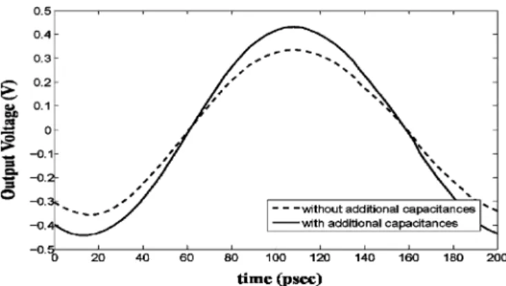
Additional capacitances C –C in parallel with cross-couple devices (M and M , M and M ) are used to increase the amplitude of the oscillator outputs waveform. These cross-couple devices are used to provide the negative differential re-sistance. Fig. 3 shows the simulated result of the outputs am-plitude of the proposed QVCO with and without the additional capacitances C –C . We can see that the amplitude with C –C is 26% larger than the one without the additional capacitances, therefore, the phase noise of the proposed QVCO can further be improved.
Fig. 2. (a) Proposed QVCO using symmetrical tail current-shaping technique. (b) the simulated currents waveform of tail transistor pairs (I and I ) and switching path I . (c) the simulated tail currents waveform (I (2') and I (2')).
Fig. 3. Simulated result of the outputs amplitude of the proposed QVCO with and without the additional capacitances C –C .
SHEN et al.: A LOW PHASE NOISE QUADRATURE VCO USING SYMMETRICAL TAIL CURRENT-SHAPING TECHNIQUE 401
Fig. 4. Chip photograph of the fabricated QVCO.
Fig. 5. VCO1 is the simulated phase noise of the proposed QVCO without the switching path I . VCO2 is the measured and simulated results of the QVCO with path I at the oscillation frequency of 5.3 GHz.
III. MEASUREMENT
The proposed QVCO was design and fabricated using the TSMC 0.18 m mixed-signal/RF CMOS 1P6M technology. Fig. 4 shows the chip photograph of the fabricated QVCO with a chip area of 0.7 1.1 mm . The bias-tee was adopted while doing measurement. The output spectrum and phase noise was measured using the Agilent E4440A spectrum analyzer and Agilent E5052A signal source analyzer, respectively.
Fig. 5 compares the measured phase noise of our proposed QVCO with switching path I3 with the simulation result of the QVCO without path I3 at the oscillation frequency of 5.3 GHz. The phase noise shows the trend of at offset frequency be-tween 100 KHz to 10 MHz, and the measured phase noise of our proposed QVCO is dBc/Hz at 1 MHz offset frequency, which is 4 dB lower than the simulated QVCO without path I at 1 MHz offset frequency.
As shown in Fig. 6 the oscillation frequency can be tuned from 5.3 GHz to 5.44 GHz as the control voltage V is raised from 0 V to 3 V, and the total tuning range is 550 MHz. The power consumption of the QVCO core is measured to be 11.2 mW at the V supply voltage of 1.4 V. The average output phase error is about . Fig. 7 shows the measured frequency spectrum of the proposed QVCO. The output power is about dBm at 5.3 GHz oscillating frequency.
Fig. 6. Measured tuning range of the proposed QVCO.
Fig. 7. Measured frequency spectrum of the proposed QVCO.
IV. CONCLUSION
A new technique to improve the phase noise of the first-har-monic injection-locking QVCO has been proposed and successfully demonstrated. The asymmetrical tail current can be eliminated with the additional switching path, and the phase noise thus can be improved by 4 dB. The measured phase noise is around dbc/Hz and dBc/Hz at 100 KHz and 1 MHz offset frequency, respectively. This low phase noise QVCO demonstrates a FOM of dB at 5.28 GHz [1].
ACKNOWLEDGMENT
The authors would like to thank the Staff of the CIC for the chip fabrication and technical support.
REFERENCES
[1] B. Soltanian and P. R. Kinget, “Tail current-shaping to improve phase noise in LC voltage-controlled oscillators,” IEEE J. Solid-State
Cir-cuits, vol. 41, no. 8, pp. 1792–1802, Aug. 2006.
[2] T. H. Huang and Y. R. Tseng, “A 1 V 2.2 mW 7 GHz CMOS quadra-ture VCO using current-reuse and cross-coupled transformer-feedback technology,” IEEE Microw. Wireless Compon. Lett., vol. 18, no. 10, pp. 698–700, Oct. 2008.
[3] S. L. Jang, S. S. Huang, C. F. Lee, and M. H. Juang, “CMOS quadra-ture VCO implemented with two first-harmonic injection-locked os-cillators,” IEEE Microw. Wireless Compon. Lett., vol. 18, no. 10, pp. 695–697, Oct. 2008.
[4] H. H. Hsieh and L. H. Lu, “A high-performance CMOS voltage-con-trolled oscillator for ultra-low-voltage operations,” IEEE Trans.
Mi-crow. Theory Tech., vol. 55, no. 3, pp. 467–473, Mar. 2007.
[5] A. Hajimiri and T. H. Lee, “A general theory of phase noise in electrical oscillator,” IEEE J. Solid-State Circuits, vol. 33, no. 2, pp. 179–194, Feb. 1998.