國
立
交
通
大
學
電子工程學系 電子研究所碩士班
碩 士 論 文
利用雙重微影成像法製作多晶矽鰭式場效電晶體元件之特
性研究
A Study on the Device Characteristics of Polycrystalline Silicon
FinFETs Fabricated
with Double Patterning Technique
研 究 生:周涵宇
指導教授:林鴻志 博士
黃調元 博士
利用雙重微影成像法製作多晶矽鰭式場效電晶體元件
之特性研究
A Study on the Device Characteristics of Polycrystalline
Silicon FinFETs Fabricated
with Double Patterning
Technique
研 究 生:周涵宇 Student :Han-Yu Chou 指導教授:林鴻志 博士 Advisors:Dr. Horng-Chih Lin
黃調元 博士 Dr. Tiao-Yuan Huang
國 立 交 通 大 學
電子工程學系 電子研究所碩士班
碩 士 論 文
Submitted to Department of Electronics Engineering & Institute of Electronics College of Electrical Engineering and Computer Engineering
National Chiao Tung University in Partial Fulfillment of the Requirements
for the Degree of Master of Science
in
Electronics Engineering September 2012
Hsinchu, Taiwan, Republic of China
利用雙重微影成像法製作多晶矽鰭式場效電晶體元件
之特性研究
研究生:周涵宇 指導教授:林鴻志 博士黃調元 博士 國立交通大學 電子工程學系 電子研究所碩士班
摘要
在本篇論文中,我們利用 I 射線(I-line)光學步進機與雙重微影成像法來製作 P 通道多晶矽鰭式場效電晶體(FinFET)。這種新穎的雙重微影成像技術不僅能夠 製作出鰭寬度(fin width)與閘極長度(gate length)小到 80nm 的多晶矽鰭式場效電 晶體且有控制良好的關鍵尺寸,並在製程上有不錯的均勻性。我們也利用準分子 雷射退火(excimer laser annealing)製程來提高多晶矽通道的品質。所 製 作 之 鰭 寬 度 80nm 的 鰭 式 場 效 電 晶 體 具 有 陡 峭 的 次 臨 界 擺 幅
(subthreshold swing, 255mV/dec) 、 高 的 開 關 電 流 比 (109) 、 與 低 的 漏 電 流
(<10-14A),歸因於它較窄的鰭通道受到閘極良好的控制。另外,我們發現當元件
的閘極長度等於或大於0.4μm 時,晶界缺陷將顯著地影響次臨界擺幅;但是當閘
極長度微縮至 0.2μm 或更小時,短通道效應(short channel effect)將主導次臨界擺 幅的趨勢。
接著探討通道厚度 50nm 之低的高寬比(aspect ratio)元件。雖然低高寬比元件 閘極的控制能力較差導致明顯的短通道效應;但是它們比通道厚度 100nm 之高 的高寬比元件有較高的載子移動率與驅動電流,因其具有優良的準分子雷射退火 結晶化條件。我們也探討了固相結晶法(solid phase crystallization)與準分子雷射退
火兩者之鰭式場效電晶體的元件特性之差別。雖然固相結晶元件的電性比準分子 雷射退火元件還差,但是它們電性的均勻性較準分子雷射退火元件為佳。
A Study on the Device Characteristics of
Polycrystalline Silicon FinFETs Fabricated
with
Double Patterning Technique
Student: Han-Yu Chou Advisors: Dr. Horng-Chih Lin
Dr. Tiao-Yuan Huang
Department of Electronics Engineering and Institute of Electronics National Chiao Tung University, Hsinchu, Taiwan
Abstract
In this thesis, we have developed a novel method which employs an I-line
stepper and double patterning (DP) technique to fabricate p-channel poly-Si FinFETs
for the first time. This novel DP technique is capable of not only generating fin widths
(Wfin) and gate lengths (Lg) of poly-Si FinFETs down to 80nm with good critical
dimension control, but also providing good process uniformity. We also use the
excimer laser annealing (ELA) process to achieve high-quality poly-Si channels.
The fabricated FinFETs with Wfin of 80nm have steep subthreshold swing (SS,
255mV/dec), high Ion/Ioff current ratio (109), and low leakage current (<10-14A)
owing to its narrow fin which enabls a better gate control over the channel. In addition,
devices when the Lg is equal to or larger than 0.4μm, but the short-channel effects
(SCEs) dominate the trend of SS as devices are downscaled to Lg of 0.2μm and
beyond.
The low aspect ratio (AR) devices with channel thickness (TSi) of 50nm were
also investigated and compared with devices with TSi of 100nm. Although the low AR
devices have poorer gate controllability and exhibit obvious SCEs, they have higher
mobility and drive current over the high AR devices with TSi of 100nm due to better
crystallization results of ELA process. The differences in device characteristics
between solid phase crystallization (SPC) and ELA FinFETs are also investigated.
Although the SPC devices have poorer electrical characteristics than the ELA devices,
Acknowledgement
短短兩年的碩士生涯即將結束,要感謝的人真的很多。首先誠摯的感謝我的 指導教授林鴻志老師與黃調元老師。感謝你們在研究上的熱心指導,研究方向也 帶給我很多的機會,讓學生受益許多;且老師們的做事嚴謹態度與謙恭溫和的待 人處事,讓我在往後的人生道路上將受用無窮。 感謝實驗室的學長姐們讓我學習很多。感謝林政頤學長(阿毛)在實驗上的指 導,並幫我解決許多實驗失敗,除了帶我做實驗量測分析外還有一起打工掃地 等,可謂名副其實的老大呢。感謝蔡子儀學長在實驗上給了我許多建議,且常找 我們去健身房運動。還有感謝謝博璿學長(阿莫)在實驗上的相助,能常跟我們這 屆一同出遊真是件青春洋溢的事。感謝郭嘉豪學長(maca)在 NDL 的幫忙,還要感 謝林哲民學長(阿民)、李克慧學姐、鍾嘉文學長、呂榮哲學長等在知識上的傳承。 還有謝謝 NDL 工程師們在實驗上的幫忙。 感謝這兩年來一起學習且共患難共玩樂的實驗室夥伴們。感謝最正的余曉惠 (村長),常策劃出許多青春瘋狂熱血有趣好玩的活動帶給我們活力與朝氣。感謝 正妹彭梵懿(彭彭),每次都很夠義氣的吃喝玩樂說走就走不愧是六年來的好同 學。感謝最帥的陳盈宇(帥棒子),除了打桌球籃球外也常找我去健身房訓練那結 實的肌肉,你真的很帥又性感。感謝帥哥林廷燿(西吉),不管實驗或生活上常跟 我討論或給我提醒,當了一個月的室友已感受到你真是位貼心的好男人。感謝正 妹張維真(小仙女),你那超快的實驗論文進度總是給我勉勵自己的動力。感謝實 驗室的學弟妹們明鴻、佳文、維軒、信宏、湘婷、靜玲、浩君一年來的陪伴與歡 笑,祝你們實驗都能順利。 感謝我的好室友博鈞、白諭,有幸能與你們共度碩班的時光,還有感謝親切 的房東先生與太太。感謝閒暇時一起玩樂的好同學海哥、阿三,常一起八卦嘴砲 抬槓讓我生活中增添了許多趣事。感謝一個月的好室友柏文、致緯、瑞銘,能一 起去長灘島畢旅真是件瘋狂有趣的事。感謝電子所的同學們,實驗之餘還能一起 吃飯聊天,祝你們未來都能成就自己的夢想。 最後要感謝我摯愛的家人。特別感謝爸媽從小的教育養成,並伴我渡過生活 中的困難;有了你們的關心與支持,讓我能勇敢的面對許多事。還有感謝弟弟、 芯羽、與可愛的恩恩,有了你們的陪伴讓我生活中增添了許多色彩。謝謝默默支 持我的家人們,也謝謝所有關心或幫助過我的人,讓我順利的完成碩士生涯。 周涵宇 誌於風城交大 2012 年 9 月Contents
Abstract (Chinese) ... I Abstract (English) ... III Acknowledgement ... V Contents ... VI Figure Captions ... VIII Table Captions ... XII
Chapter 1 Introduction
1.1 Overview of Multi-gate and FinFET Technology ... 1
1.2 Double Patterning Technique ... 2
1.3 Overview of Low Temperature Polycrystalline Silicon Thin Film Transistors (LTPS TFTs) ... 4
1.3.1 Solid Phase Crystallization (SPC) ... 5
1.3.2 Excimer Laser Annealing (ELA) ... 6
1.4 Motivation ... 6
1.5 Thesis Organization ... 7
Chapter 2 Device Structure and Process Flow
2.1 Device Fabrication and Process Flow ... 82.2 Feasibility of Double Patterning Technique ... 9
2.3 Electrical Measurement Setup ... 12
Chapter 3 Results and Discussion
3.1 Basic Electrical Characteristics of P-channel FinFETs ... 143.2 Device Characteristics of Various Channel Structure ... 17
Chapter 4 Conclusion and Future Work
4.1 Conclusion ... 24
4.2 Suggestions for Future Work ... 26
References
... 28Figures
... 33Tables
... 59Vita
... 61Figure Captions
Chapter 1
Fig. 1-1 2009 ITRS gate length trends of microprocessor unit (MPU) ... 33 Fig. 1-2 The 3-D view of a TG FinFET structure ... 33
Chapter 2
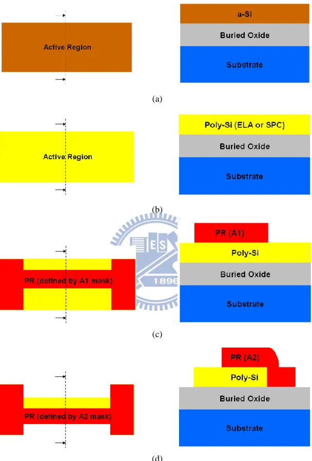
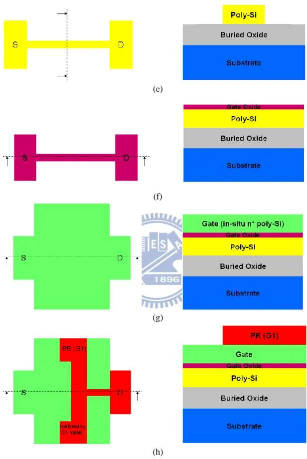
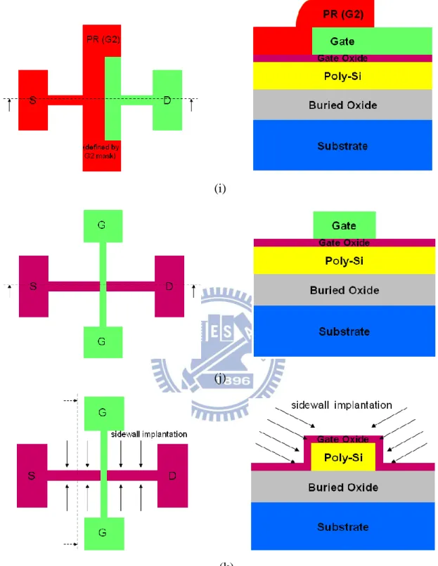
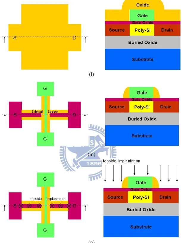
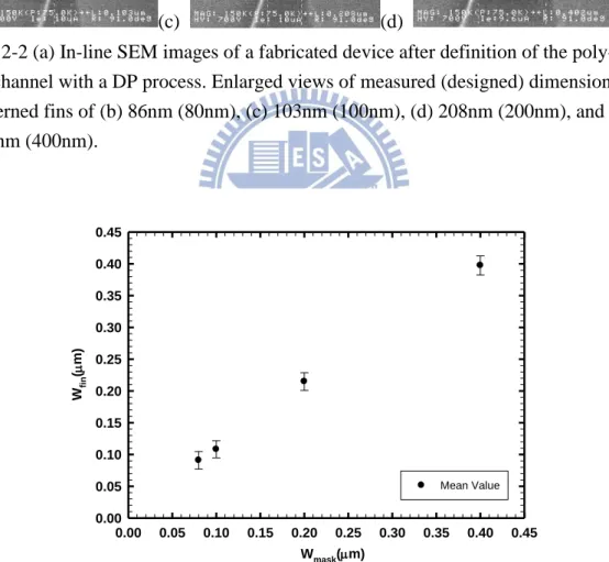
Fig. 2-1 (a)-(n) Process flow of p-channel FinFETs with double patterning technique. The left-hand-side figures are top views, and the right-hand-side figures are cross-sectional views. ... 34 Fig. 2-2 (a) In-line SEM images of a fabricated device after definition of the poly-Si
fin channel with a DP process. Enlarged views of measured (designed) dimension of patterned fins of (b) 86nm (80nm), (c) 103nm (100nm), (d) 208nm (200nm), and (e) 402nm (400nm)... 38 Fig. 2-3 Practical fin width (Wfin) extracted by in-line SEM versus the designed fin
width (Wmask). The error bar is the standard deviation (1-σ) of the measured
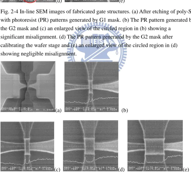
data. ... 38 Fig. 2-4 In-line SEM images of fabricated gate structures. (a) After etching of poly-Si with photoresist (PR) patterns generated by G1 mask. (b) The PR pattern generated by the G2 mask and (c) an enlarged view of the circled region in (b) showing a significant misalignment. (d) The PR pattern generated by the G2 mask after calibrating the wafer stage and (e) an enlarged view of the circled region in (d) showing negligible misalignment . ... 39
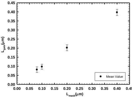
Fig. 2-5 (a) In-line SEM images of a fabricated device after definition of the poly-Si gate with a DP process. Enlarged views of measured (designed) dimension of patterned gates of (b) 70nm (80nm), (c) 93nm (100nm), (d) 196nm (200nm), and (e) 398 (400nm) ... 39 Fig. 2-6 Practical gate length (Lgate) extracted by in-line SEM versus the designed
gate length (Lmask). The error bar is the standard deviation (1-σ) of the
measured data... 40 Fig. 2-7 Measured gate lengths (Lgate) of the gate with designed gate lengths (Lmask)
of 200 nm varies with the widths of the fin channel (Wfin). (a) Wfin 80nm,
Lgate 182nm, (b) Wfin 200nm, Lgate 180nm, (c) Wfin 400nm, Lgate 163nm, and
(d)Wfin 1000nm, Lgate 149nm ... 40
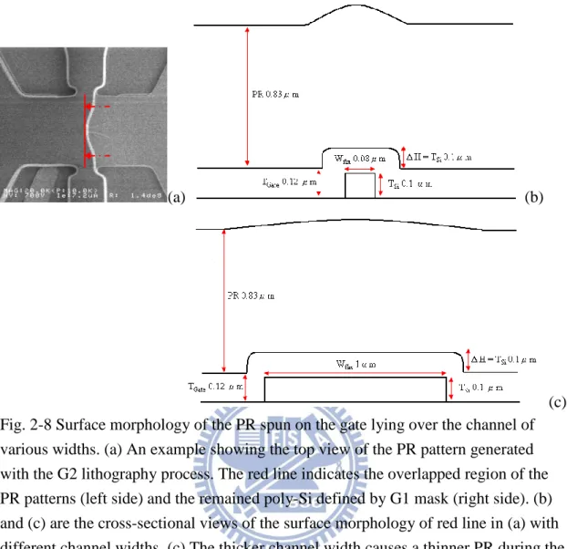
Fig. 2-8 Surface morphology of the PR spun on the gate lying over the channel of various widths. (a) An example showing the top view of the PR pattern generated with the G2 lithography process. The red line indicates the overlapped region of the PR patterns (left side) and the remained poly-Si defined by G1 mask (right side). (b) and (c) are the cross-sectional views of the surface morphology of red line in (a) with different channel widths. (c) The thicker channel width causes a thinner PR during the action of spinning . ... 41 Fig. 2-9 Cross-section TEM graphs of ELA poly-Si channel with designed Wmask =
TSi = 100nm. Practical fin widths (Wfin) and channel thickness (TSi) were
measured to be 132nm and 94nm, respectively. ... 41
Chapter 3
Fig. 3-2 Electrical characteristics of (a) Id-Vg and (b) Id-Vd with fin width of 0.08μm
and gate length of 0.4μm ... 42 Fig. 3-3 Transfer characteristics of devices with gate length of 0.2μm and various fin widths (Wfin) ranging from 0.08 to 1μm, (a) un-normalized drain current ,
and (b) drain current normalized to the effective fin widths (Weff) ... 43
Fig. 3-4 Transfer characteristics of devices with gate length of 0.4μm and various fin widths (Wfin) ranging from 0.08 to 1μm, (a) un-normalized drain current ,
and (b) drain current normalized to the effective fin widths (Weff) ... 44
Fig. 3-5 Transfer characteristics of devices with gate length of 1μm and various fin widths (Wfin) ranging from 0.08 to 1μm, (a) un-normalized drain current ,
and (b) drain current normalized to the effective widths (Weff) ... 45
Fig. 3-6 Transfer characteristics of devices with same fin width of 0.08μm and various gate lengths ranging from 1 to 0.08μm ... 46 Fig. 3-7 Mean value and standard deviation of threshold voltage (Vth) as a function
of the channel length for devices with various Wfin ... 46
Fig. 3-8 Mean value and standard deviation of subthreshold swing (SS) as a function of channel length for p-FinFETs ... 47 Fig. 3-9 Transfer characteristics for devices with channel lengths of 0.4μm and 0.2μm . ... 47 Fig. 3-10 Typical transfer characteristics of devices with gate length of 1μm and various fin widths (Wfin) ranging from 0.08 to 1μm. The drain current is
normalized to the effective fin widths (Weff) ... 48
Fig. 3-11 Typical transfer characteristics of devices with gate length of 0.4μm and various fin widths (Wfin) ranging from 0.08 to 1μm. The drain current is
of the channel length for devices with various Wfin ... 49
Fig. 3-13 Typical transfer characteristics of devices measured at Vd = -0.5 and -1.5 V
with gate length of 0.4μm and fin widths (Wfin) ranging from 0.08 to
1μm . ... 49 Fig. 3-14 Mean value and standard deviation of subthreshold swing (SS) as a function of channel length ... 50 Fig. 3-15 Electrical characteristics of (a) Id-Vg and (b) Id-Vd for devices with the same
effective fin width (Weff) but different TSi and Wfin ... 51
Fig. 3-16 Mobility of the devices characterized in Fig. 3-15 ... 52 Fig. 3-17 Re-crystallization schemes as the a-Si film is irradiated with excimer laser irradiation. (a)-(c) are partial-melting process occurring in a thicker film, and (d)-(f) are near-complete-melting process occurring in a thinner film . ... 53 Fig. 3-18 Measured series resistance (Rm) and the extracted source/drain resistance
(RSD) of the devices with different channel thickness (TSi) of (a) 100nm and
(b) 50nm ... 54 Fig. 3-19 Transfer characteristics for devices with Weff of 0.3 and 0.6μm and Lg =
0.4μm ... 55 Fig. 3-20 Electrical characteristics of (a) Id-Vg and (b) Id-Vd for SPC and ELA
devices ... 56 Fig. 3-21 Mobility of the SPC and ELA devices ... 57 Fig. 3-22 Mean value and standard deviation of threshold voltage (Vth) as a function
of the channel length for the SPC and ELA devices with Wfin of 80nm ... 57
Fig. 3-23 Mean value and standard deviation of subthreshold swing (SS) as a function of channel length for the SPC and ELA devices with Wfin of 80nm ... 58
Table Captions
Chapter 2
Table 2-1 Split conditions of channel thickness (TSi) and oxide thickness (Tox) for
ELA and SPC FinFETs. ... 59
Table 2-2 Dimensions of designed gate length (Lmask) and fin width (Wmask) with
double patterning process ... 59
Table 2-3 Specifications of the Canon FPA-3000i5+ Stepper ... 59
Table 2-4 Measured gate lengths (Lgate) of various designed dimension on fin channel
of various widths (Wfin). The data were measured from structures located
Chapter 1
Introduction
1.1 Overview of Multi-gate and FinFET Technology
The invention of transistors has resulted in a tremendous impact on human’s life,
and the semiconductor industry has been playing a key role for advancing the science
and technology in the last few decades. To achieve high performance, high device
density, low power dissipation, and low manufacturing cost of CMOS circuits, scaling
down the semiconductor devices is necessary. According to Moore’s Law, the number
of devices on a circuit doubles approximately every two years [1]. Although the
predicted period seems not so precise, overall the trend has continued for half a
century. However, the 2010 update of International Technology Roadmap for
Semiconductors (ITRS) has announced that device density doubles only every three
years at the end of 2013 and many difficult challenges for further scaling are
emerging [2]. As the gate length of MOS devices shrinks down and approaches the
physical limitation (Fig. 1-1), several major challenges are lying ahead, such as short
channel effects (SCEs), leakage currents, and reliability, etc. These problems will
degrade the device characteristics. Therefore, non-classical device structures have
been explored to deal with these issues aimed at enabling continued scaling [3].
multiple-gated (MG) structure in which the non-planar channel region is controlled by
a gate wrapping around has been attracting much attention [4]. Devices adopting the
MG structure can suppress the penetration of the drain electric field into the channel.
Therefore, MG transistors can increase the gate controllability over the channel in
order to suppress the SCEs. Among the MG transistors, Fin-type MOSFET (FinFET),
which was proposed by Hisamoto in 1989 [5] and Hu in 1998 [6], is considered as
one of the most promising devices. Several types of FinFET structures have been
developed, such as double-gate (DG) [7], tri-gate (TG) [8], and Ω-gate [9]. The TG
structure of a FinFET is shown in Fig. 1-2. In the scheme, the active channel is
patterned to form a fin-like structure and the gate wraps both the top and side surface
of the fin [10]. Such a scheme can reduce bulk leakage current due to good
electrostatic control on channel potential. It can also promote the current density per
unit planar width considering the adoption of vertical channel regions. Additionally,
the quasi-planar structure of FinFETs is compatible with the conventional MOSFET
process technology [11]. In 2011, Intel announced that it will use FinFETs in its 22
nm-node manufacturing of microprocessors in 2012 [12]. Therefore, the FinFET has
been perceived as a promising device for the 22 nm technology node and beyond.
When the devices shrink in size, advanced lithography technique is essential to
keep the Moore’s Law. The resolution R of a lithography process follows the Rayleigh
theory [13], which can be expressed as:
NA K
R 1 (1-1), where K1 is a system constant, λ is the wavelength of the light, and NA is the
numerical aperture. We can modulate these variables of Rayleigh equation in order to
achieve higher resolution for shrinking the feature size. Many lithographic
technologies have been developed to reduce K1 factor, such as off-axis illumination
(OAI), phase shift mask (PSM), optical proximity correction (OPC), and immersion
technology. Additionally, the reduction of wavelength can also improve resolution.
For instance, the progress of light sources of lithography tools has evolved from
G-line (436nm), I-line (365nm), KrF excimer laser (248nm), to ArF excimer laser
(193nm). However, the finer resolution is acquired at the expense of incredible
development cost. The e-beam and ion-beam lithography systems have also been
proposed because of their capability to achieve a fine resolution, but the extremely
low throughput prevents them from being adopted in practical manufacturing [14].
The double patterning (DP) technique is a potential way to improve resolution
and theoretically it can cut the pitch in half with currently available tools. A typical
DP has additional mask and etching process cost, it can maintain a good throughput.
Actually the DP method with 193 nm immersion lithography has been adopted by the
IC manufacturers in the 32 nm node in recent years [16]. However, these advanced
lithography facilities for generating nano-scale patterns are very costly and not
available for the studies conducted in academic organizations. Nonetheless, sub-100
nm patterns can also be readily achieved with an I-line stepper [17]. In this study,
such DP technique using an I-line stepper is adopted to fabricate FinFETs.
1.3 Overview of Low Temperature Polycrystalline Silicon
Thin Film Transistors (LTPS TFTs)
In the past decades, amorphous silicon thin film transistors (a-Si TFTs) had been
used as the switching device of pixels in the active-matrix liquid-crystal displays
(AMLCDs) [18]. A-Si TFTs possess low leakage current and low process
temperatures. However, the carrier mobility of a-Si TFTs (<1 cm2/V-s) is much lower than that of polycrystalline silicon (poly-Si) TFTs (10-500 cm2/V-s) [19]. In order to integrate high-performance driver circuits on the same display panel,
low-temperature-processed poly-Si TFTs were actively developed recently. Poly-Si
TFTs have the advantages of high driving current, good device reliability, and low
of displays but also have the potential for construction of 3-dimentional integrated
circuits [20].
In addition, the low temperature polycrystalline silicon (LTPS) fabrication
process plays an important role in the crystallization of the poly-Si thin films from
a-Si, and the quality of crystallized poly-Si thin films has a great influence on the
performance of LTPS TFTs. In order to improve the quality of the poly-Si thin films
and reduce the cost of process, there are several LTPS technologies developed, such
as solid phase crystallization (SPC) [21], excimer laser annealing (ELA) [22], and
metal induced lateral crystallization (MILC) [23]. The SPC and ELA methods are
used in this work and will be introduced in the following sub-sections.
1.3.1 Solid Phase Crystallization (SPC)
The SPC is a commonly used method to transform the a-Si thin film into poly-Si
thin film by thermal annealing. The annealing temperature is around 600℃ in N2
ambient, and the process time is about 24 hours [24]. However, the annealing time is
long and will limit the throughput of device fabrication. In addition, the quality of an
SPC poly-Si thin film is affected by its small grain size because the abundant defects
located in or close to the grain boundaries, such as intra-grain strained bonds and
inter-grain dangling bonds, tend to impede the carrier transport and formation of the
1.3.2 Excimer Laser Annealing (ELA)
Recently, the ELA has become the most promising crystallization method in the
fabrication of LTPS TFTs [25]-[26]. Types of the excimer lasers include ArF, KrF, and
XeCl (wavelengths are193, 248, and 308nm, respectively) gaseous discharges. Due to
the short pulse duration time (typically 10-30ns) of the irradiation and large
absorption coefficients of a-Si thin film to UV lights, ELA process can confine the
heat to the silicon thin film and avoids the thermal damage to the underlying glass
substrate [27]. In the ELA process, the phase transformation from a-Si to poly-Si
occurs by melting the silicon thin films. As the laser energy exceeds a threshold
energy, the irradiated a-Si thin film melts and then solidifies into large grains in a very
short time [28]. As a result, the high quality and large-grained poly-Si thin films can
be achieved with less defects and high throughput.
1.4 Motivation
The aforementioned merits of FinFET structure, such as enhanced gate
controllability and reduction of the total amount of defects contained in the tiny fin
channel, are expected to improve the performance of LTPS devices. As the
conduction width of a FinFET is approximately the sum of the side and the top
surface dimensions, this vertical feature can be optimized by increasing the aspect
Moreover, FinFETs will show improved SCE control when the fin width is scaled,
and the improvement in device density might also be achieved [29].
In this work, we have developed a method which employs an I-line stepper and
double patterning (DP) technique to fabricate p-channel poly-Si FinFETs for the first
time. Both the fin and gate are defined by DP lithography and conventional dry
etching. Since defects in the poly-Si channel will adversely affect device
characteristics, to reduce the defects, we use the ELA process to achieve high quality
of poly-Si thin films with low-temperature process.
1.5 Thesis Organization
This thesis is divided into four chapters. In Chapter 1, the background and
motivation of poly-Si FinFETs technology are already given above. In Chapter 2, the
process flow of FinFETs is described in detail. We monitored the DP process with
in-line SEM analysis during the device fabrication. In Chapter 3, we present the
electrical characteristics of the fabricated P-channel FinFETs. The characteristics of
FinFETs with various channel dimensions and crystallization method are compared
and discussed. Finally, in Chapter 4, we conclude the results and suggest the future
Chapter 2
Device Structure and Process Flow
2.1 Device Fabrication and Process Flow
The process steps of FinFET fabrication are described as follows, and the
fabrication process for the proposed device is shown in Fig. 2-1. First, a 1000nm-thick
wet oxide was grown on six-inch silicon wafers to serve as the buried oxide. Next, an
a-Si layer was deposited by low-pressure chemical vapor deposition (LPCVD) at 550℃
(Fig. 2-1(a)), and the a-Si thickness was split into 50nm and 100nm. Then, the 50
nm-thick a-Si thin films and part of the 100 nm-thick ones were transformed into
polycrystalline by excimer laser annealing (KrF, 480 mJ/cm2), and the remaining 100nm-thick a-Si thin film was transformed into polycrystalline by solid phase
crystallization at 600℃ in N2 ambient for 24 hours (Fig. 2-1 (b)). Afterwards, the
poly-Si thin film was defined by the A1 and A2 masks with the double patterning (DP)
technique (Figs. 2-1 (c) to (e)) to form the active channel regions.
A TEOS-oxide layer was then deposited as gate oxide by LPCVD (Fig. 2-1 (f)),
and the gate oxide thickness was either 10nm or 30nm. Subsequently, a 120nm-thick
in-situ n+ poly-Si layer was deposited by LPCVD to serve as the gate electrode (Fig. 2-1 (g)). Afterwards, the gate electrode was defined by the G1 and G2 masks with
The first BF2+ ion implantation was used to dope the sidewalls of p+ source/drain
for p-channel FinFETs with 10-nm thick gate oxide (at 30keV, 1×1014 cm-2, tilt angle =60°) or 30-nm thick gate oxide (at 54keV, 1×1014 cm-2, tilt angle =60°),as shown in Fig. 2-1 (k). A 55nm-thick TEOS-oxide layer was deposited by LPCVD (Fig. 2-1 (l)),
followed by a dry etching step to form the spacer (Fig. 2-1 (m)), whose width is about
38nm. Afterwards, the second self-aligned BF2 ion implantation was used to dope the
topside of p+ source/drain with split of 10-nm thick gate oxide (at 25keV, 5×10¹⁵
cm-2, tilt angle =0°) and split of 30-nm thick gate oxide (at 46keV, 5×1015 cm-2, tilt angle =0°), respectively, as shown in Fig. 2-1 (n), followed by rapid thermal annealing
(RTA) at 850℃ for 5 seconds. Finally, the passivation layer deposition, contact hole
opening, metallization, and H2 sintering processes were done to complete the
fabrication of FinFETs.
The split conditions of the fabricated FinFETs are summarized in Table 2-1.
Dimensions of both designed gate length (Lmask) and fin width (Wmask) with double
patterning process are shown in Table 2-2.
2.2 Feasibility of Double Patterning Technique
As described in previous section that both the fins and gates were defined by the
patterns, and employed an in-line scanning electron microscope (SEM) and
transmission electron microscopy (TEM) to check the fabricated structures of the fins
and gates. In Fig. 2-1 (c), the PR pattern generated by the A1 mask is used to
preliminarily define the active channel region with the first etching process, and then
the PR pattern generated by the A2 mask covers portion of the active channel region
(e.g., the bottom half of the active region, as shown in the top view of Fig. 2-1 (d)).
After the second etching process, the overlapped region of A1 and A2 masks defines
the final fin channel (Fig. 2-1 (e)).
Figures 2-2 (a) to (d) show the in-line SEM images of the etched poly-Si fins
achieved with the DP method. These images obviously evidence that the DP can
reliably shrink the poly-Si fin width down to sub-100 nm scale. The results and
variations of fin widths are shown in Fig. 2-3 by measuring samples of different
designed fin width (Wmask) taken from different locations of the Si wafers. These
results confirm that the DP method is capable of not only generating fins with width
down to 80 nm and good critical dimension (CD) control, but also providing good
process uniformity.
We use another DP process to define the gated region. In Fig. 2-4 (a), the
remained poly-Si in the right side is defined using the G1 mask. PR generated by the
can obviously see that a misalignment between the PR and underlying poly-Si occurs
in the circled region. An enlarged view of this region is shown in Fig. 2-4 (c), from
which we can see that the misalignment is around 84nm, much larger than the overlay
spec. of the I-line stepper (Table 2-3). This indicates that the dimensions of the
patterns on G1 and G2 masks may deviate from the designed values and lead to the
observed misalignment. The aforementioned glitch is likely to be resulted during the
manufacturing of the masks considering the fact that the etching of the patterns was
done with manual wet processing.Fortunately this issue can be addressed by shifting
the wafer stage of the stepper by -80nm along the horizontal direction in the figure
during exposure to compensate for the misalignment. Results after implementing the
measure are shown in Figs. 2-4 (d) to (e). Obviously the above method works well
from the good alignment shown in the figures.
Figures 2-5 (a) to (d) show the in-line SEM images of the poly-Si gates of
different dimensions patterned with the 2nd DP process. The variations of gate lengths taken from different locations of the Si wafers are shown in Fig. 2-6. Still, good
controls over the gate CD down to 80 nm and uniformity are achievable.
In the gate DP process, we find that the widths of the fin channel beneath the
gate electrode will affect the resulted gate lengths. Table 2-4 summarizes the
different widths. The data were collected from structures located in the same die.It is
seen that the measured gate length decreases as fin width increases. In-line SEM
images of a set of samples with Lmask of 200 nm are shown in Fig. 2-7. This finding is
postulated to be related to the different surface morphology of the PR spun on the gate
lying over the channel of various widths. As shown in Fig. 2.8, the thickness of the
PR gets thinner as the channel width is increased due the action of spinning.A thinner
PR would lead to a finer pattern after exposure, as the finding shown above.
Fig. 2-9 shows the cross-section TEM graph of an ELA poly-Si channel, and the
measured channel fin width (Wfin) and thickness (TSi) are 132nm and 94nm,
respectively, which are smaller than the grain size of ELA poly-Si channel
(0.3~0.5μm) [30]. With such a fine channel structure, it is expected that no or only
one single grain boundary will be contained in the channel region as the channel
length is scaled below half a micron regime. The fabricated devices would thus
exhibit high performance but with a high fluctuation.
With in-line SEM and TEM analysis, we can confirm the capability of this novel
lithography technique in the fabrication of sub-100 nm FinFET devices.
2.3 Electrical Measurement Setup
performed by a measurement system which consists of an HP-4156A semiconductor
parameter for I-V measurements, an Agilent-E5250A switch, and a temperature
regulated hot-chuck for keeping the wafer temperature stable. Interactive
Characterization Software (ICS) is used to set up all measurement conditions and
Chapter 3
Results and Discussion
3.1 Basic Electrical Characteristics of P-channel FinFETs
From the Id-Vg transfer curve measured at Vd = -0.5V, the characteristics of
P-channel FinFET can be extracted as follows:
Threshold voltage (Vth) is defined by using the constant current method to be the
gate voltage (Vg) needed to achieve the drain current (Id) of 50nA×(Weff/Lg):
g eff D G th L W nA I V V @ 50 (3-1),
where Weff and Lg are effective conduction width and gate length, respectively. The
effective conduction width (Weff) of a channel is the sum of channel fin width (Wfin)
and twice the channel thickness (2×TSi), as shown in Fig. 3-1.
Subthreshold swing (SS) can be extracted from the subthreshold current with the
following form: ) ( l o gd g I V SS (3-2). Figure 3-2 shows the characteristics of electrical measurements performed on a
device with a narrow Wfin of 80 nm. The device has a steep SS (255mV/dec), a high
Ion/Ioff current ratio (109), and low leakage current (<10-14A) owing to its narrow fin
(DIBL).
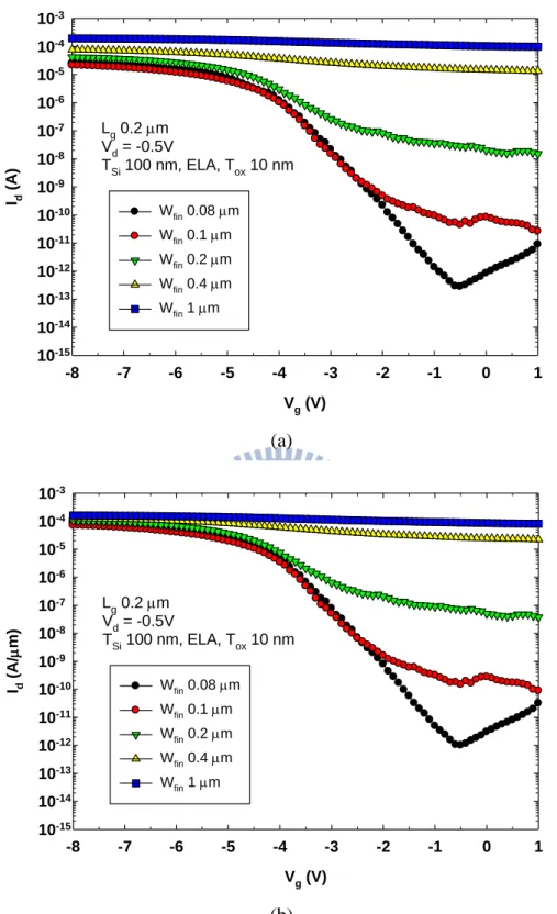
Figure 3-3 shows the transfer characteristics of the fabricated devices with gate
length of 0.2μm and various fin widths. Devices with narrow Wfin of 0.08 and 0.1μm
can achieve low SS. However, the Vth becomes more positive and the subthreshold
current increases when the fin’s width increases to 0.2μm or wider. For these wider dimensions, the “fin” channel actually becomes quasi-planar and thus the gate
controllability is degraded [31]. As a result, a significant amount of sub-surface
punch-through current would conduct and lead to a high subthreshold leakage.
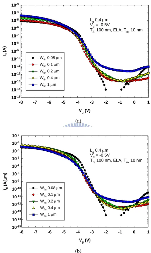
Figure 3-4 and Fig. 3-5 show the transfer characteristics of the fabricated devices
with gate length of 0.4μm and 1μm, respectively, and various Wfin. The leakage
current of these long channel devices is much lower than that of the device with gate
length of 0.2μm because of reduced SCE. In Fig. 3-4, the SS decreases as Wfin
decreases because of better gate controllability. In Fig. 3-5, the leakage current
increases as Wfin increases owing to the larger sub-surface leakage current.
Figure 3-6 shows the transfer characteristics of devices having the Wfin of 80 nm
with various gate lengths (Lg). The devices with longer gate lengths of 0.2, 0.4, and
1μm have good Ion/Ioff current ratio of about 108 to 109. Nonetheless, the Ion/Ioff current
ratio is smaller than 10 when the Lg is equal to or smaller than 0.1μm. Obviously here
channel occurs [32]. To improve the transfer characteristics of the short-channel
devices, it requires a refined S/D annealing scheme with a tighter control over the
thermal budget to suppress the undesirable dopant diffusion.
In Fig. 3-6, the SS of Lg of 0.4μm device is better than that of the Lg of 1μm
device, which is in conflict with the trend of SCE. The following equation is the relation between the SS and the effective trap-state concentration (Ntrap) for poly-Si
TFTs: ) 1 ( 10 ln ox T C C q kT SS (3-3), where CT qNtrapWd, and Wd is the effective depletion width. The grain size of
ELA poly-Si channel is about 0.3~0.5μm [30] which is comparable to the devices
with Lg of 0.4μm. Therefore, the number of the grain boundaries could be small and
even zero. This would reduce the trap-state concentration and result in better SS over
the devices with Lg of 1μm. The Vth roll-off is shown in Fig. 3-7. Since the Vth roll-off
from Lg of 1μm to Lg of 0.4μm devices is unobvious, the grain boundary defects
would predominantly affect the SS in the devices. Fig. 3-8 shows the SS of the
devices with various Wfin as a function of Lg. As it can be seen in the figure that the
SS of the devices with Lg of 0.4μm is very sensitive to Wfinand tends to decrease as
Wfin is shortened. Two reasons are responsible for such a trend. One is the
printed channel length. The other is the greatly enhanced gate controllability over the
channel as the fin is scaled to nano-scale. In Fig. 3-7 the Vth roll-off is obvious
because of SCE, and the SS is the worst in Fig. 3-8. From Fig. 3-9, we confirm that
the devices with Lg of 0.2μm exhibit large DIBL, contrary to the devices with Lg ≧
0.4μm whose DIBL is negligible. The results evidence that SCE dominates the trend of SS as devices are downscaled to Lg of 0.2μm and beyond.
The dimension of Wfin of 0.08μm is much smaller than the ELA poly-Si grain
size (0.3~0.5μm). As mentioned above, the SS of Wfin of 0.08μm devices at Lg of
0.4μm is much lower than the devices with Wfin of 0.4μm and 1μm in Fig. 3-8.
Meanwhile, in Fig. 3-7 and Fig. 3-8, the standard deviations of both Vth and SS
characteristics increase as the Wfin decreases at the same Lg, and also increases as Lg
decreases at the same Wfin. Although a decrease in Wfin tends to better device
performance from the presented results, the uniformity of device characteristics
suffers owing to the fluctuation in structural parameters like Wfin and the grain size of
ELA poly-Si.
3.2 Device Characteristics of Various Channel Structure
Characteristics of devices with thin channel thickness (TSi) of 50nm are
of the devices with gate length of 1μm and various fin widths. The SS decreases as
Wfin decreases because of better gate controllability. Most of trap centers located at or
near the grain boundaries are charged positively as the surface potential of the channel
becomes inverted, and the threshold voltage can be expressed as [33]
ox d trap F FB th C W qN V V 2 (3-4), where Ntrap and Wd are trap state density and effective depletion width,
respectively. In Fig. 3-10 of these long channel devices, the Vth becomes more
negative as the Wfin increases because wider Wfin contains more poly-Si grain
boundaries (and thus higher Ntrap). A reduction in Ntrap as Wfin decreases also
reflects on the higher on-current shown in the figure.
The low aspect ratio (AR, equal to TSi/Wfin) of the channel at a fixed TSileads to
the poorer gate control over the channel potential [31]. This trend is obviously shown
in Fig. 3-11, in which the transfer characteristics of the devices with gate length of
0.4μm and various fin widthsare compared. As compare with the results shown in Fig.
3-4 (b) for devices with TSi of 100nm, the SS and subthreshold leakage increase at the
same Wfin because the devices with low AR have worse gate controllability [31]. The
trend is more obvious as Wfin ≧ 0.4μm.
Figure 3-12 shows the Vth of the devices with various Wfin as a function of Lg. As
obvious because of worsened gate controllability. Meanwhile, in Fig. 3-12, the drop in
Vth with decreasing channel length is more obvious for devices with Wfin of 0.4 and
1μm than that for devices with Wfin of 0.08 and 0.2μm. Figure 3-13 shows typical
transfer characteristics of devices measured at Vd = -0.5 and -1.5 V with gate length of
0.4μm and fin widths (Wfin) ranging from 0.08 to 1μm. From the figure, we can see
the devices with Wfin of 0.4μm and 1μm exhibit larger DIBL. This confirms that
devices with wider Wfin suffer more serious SCE because of poorer gate
controllability.
Figure 3-14 shows the SS for the devices with various Wfin as a function of Lg.
The SS for devices with Lg of 0.4μm is better than that for devices with Lg of 1μm at
Wfin of 0.08 and 0.2μm. From eq. 3-3, the grain boundary defects would
predominantly affect the SS in these devices with a narrow Wfin. In contrast, for
device at Wfin of 0.4 and 1μm, the SS for devices with Lg of 0.4μm is higher than that
for devices with Lg of 1μm, which is different form that shown in Fig. 3-8 for devices
with TSi of 100nm. From Fig. 3-13, the devices with wide Wfin of 0.4 and 1μm at low
AR with TSi of 50nm have large DIBL. Fig. 3-14 evidences that SCE dominates the
trend of SS in these devices with wide Wfin and low AR.
Figure 3-15 compares the electrical characteristics of two devices with the same
devices are 100 (100) and 200 (50), respectively. The device with TSi of 100nm has
steeper SS and lower subthreshold leakage than the device with TSi of 50nm due to
improved gate controllability, but the on-current is lower than the device with TSi of
50nm. We further extract the field-effect mobility (μFE) of devices with different TSi,
and the μFE is determined by
d ox eff m g FE V C W G L (3-5),
where G is the maximum transconductance and m C is the gate capacitance per ox
unit area. As shown in Fig. 3-16, the μFE of the device with TSi of 50nm is larger than
that of the device with TSi of 100nm. The reason is postulated to be related to the ELA
condition [34]. Note that we used the same excimer laser energy (480mJ/cm2) to crystallize the a-Si films of different thickness. In the thicker TSi film of 100nm, the
laser energy might cause only surface melting of the a-Si layer rather than the entire
layer (i.e., melting depth < film thickness) [35], as schematically shown in Figs. 3-17
(a) to (c). This results in a smaller grain size and low quality of poly-Si film [36]. In
the thinner TSi film of 50nm, the laser energy causes near-complete-melting of the
thin film consisting of un-melted discrete silicon islands (i.e., melting depthfilm
thickness) [37], as shown in Figs. 3-17 (d) to (f). Because the distance between the
mobility and on-current for devices with TSi of 50nm are higher than those for the
devices with TSi of 100nm.
Figure 3-18 extracts the source/drain series resistance (RSD) of these devices with
different TSi by the total resistance method [38]:
channel SD d d m R R I V R (3-6),
where R is the measured resistance, and m Rchannel is the channel resistance. The RSD
for the devices with TSi of 100nm is about 21kΩ, which is larger than that for the
devices with TSi of 50nm (~10kΩ). Note that the implantation and annealing process
condition of devices with different TSi are the same as mentioned in last chapter. The
reduction in RSD for devices with TSi of 50nm is another reason for the higher
on-current and mobility as compared with devices with TSi of 100nm, and is attributed
partly to the larger grain size of the 50 nm-thick channel.
Figure 3-19 shows the transfer characteristics of the devices with Weff of 0.3 and
0.6μm and at the same Lg of 0.4μm. The device with Weff of 0.3μm has better SS and
lower subthreshold leakage than the device with Weff of 0.6μm because of better gate
controllability. The on-current of the device with Weff of 0.3μm is larger than that of
the device with Weff of 0.6μm because the thinner TSi contains less defects.
and ELA
A comparison in the device characteristics between SPC and ELA devices is
discussed in this section. Figure 3-20 shows the electrical characteristics of the
fabricated devices which have Tsi = 100 nm, Wfin of 80nm, and Tox = 10 or 30 nm.
Because the grain size of SPC poly-Si is smaller than that of ELA [39], the SPC
channel has more grain boundaries (GB) and thus more defects than the ELA channel.
As a result, the SS of SPC devices are worse than that of the ELA devices (refer to eq.
3-3), as shown in Fig. 3-20 (a). Also, the subthreshold leakage of SPC devices is
higher than that of the ELA devices. In Fig. 3-20 (b), the SPC device has lower drive
current than the ELA device with the same Tox of 10nm. The drive current of the ELA
device with Tox of 30nm is the lowest because of the much thicker gate oxide. The
field-effect mobility of the SPC device is lower than that of the ELA one, as shown in
Fig. 3-21, obviously due to more grain boundary defects contained.
Figure 3-22 shows the Vth roll-off characteristics of SPC and ELA devices with
Wfin of 80nm as a function of Lg. The Vth of SPC devices with Tox of 10nm, which is
comparable to the Vth of ELA devices with Tox of 30nm, becomes more negative than
that of the ELA devices with the same Tox of 10nm due to more poly-Si grain
boundaries in the SPC channel (eq. 3-4). Nonetheless, the Vth roll-off is comparable
worse Vth roll-off is observed. Figure 3-23 shows the SS of SPC and ELA devices
with Wfin of 80nm as a function of Lg. Since the Vth roll-off from Lg of 1μm to Lg of
0.4μm is not obvious in Fig. 3-22, the grain boundary defects would predominantly
affect the SS in the devices with Wfin of 80nm (eq. 3-3). Obviously here the SS of
SPC devices with Lg of 0.4μm is much poorer than those of the ELA devices with Lg
of 0.4μm, as shown in Fig. 3-23. As Lg is below 0.4 um, the SS obviously increases
for all devices due to serious SCE.
However, the standard deviations of both Vth and SS of SPC devices are lower
than those of the ELA devices with the same Wfin of 80nm, as shown in Fig. 3-22 and
Fig. 3-23.This is ascribed to the tiny grain size of the SPC poly-Si which is less than
0.1μm [39], much smaller than the grain size of ELA (0.3~0.5μm). Although an
increase in grain size of ELA poly-Si tends to better device performance, the
uniformity of device characteristics suffers owing to the fluctuation in structural
Chapter 4
Conclusion and Future Work
4.1 Conclusion
In this study, we have developed a novel method which employs an I-line stepper
and double patterning (DP) technique to fabricate p-channel poly-Si FinFETs for the
first time. We also use the ELA process to achieve high quality of poly-Si channel.
With the aid of DP technique, various devices with different fin widths (Wfin) and gate
lengths (Lgate) were fabricated and characterized in our study. The effects of grain size,
channel dimensions, and crystallization methods (SPC and ELA) on the device
characteristics were investigated.
From the in-line SEM characterization, this novel DP technique is capable of not
only generating Wfin and Lgate of poly-Si FinFETs down to 80nm with good critical
dimension control, but also providing good process uniformity. During the gate DP
process, we found that the widths of the fin channel beneath the gate electrode will
affect the resulted gate lengths. This phenomenon would affect the SCE of the devices
with shorter Lgate.
Most of the fabricated FinFETs have steep subthreshold swing (SS), high Ion/Ioff
current ratio, and low leakage current owing to its narrow fin enabling a better gate
becomes poor and the sub-surface leakage current increases, resulting in poor SS. In
addition, we found that the SS of Lg of 0.4μm device is better than that of the Lg of
1μm device because the grain-boundary defects would predominantly affect the SS in
these devices. However, the devices with Lg of 0.2μm exhibit large DIBL. Thus the
SCE dominates the trend of SS as devices are downscaled to Lg of 0.2μm and beyond.
The low aspect ratio (AR) devices with channel thickness (TSi) of 50nm were
investigated. As compared with the high AR devices with TSi of 100nm, these low AR
devices have larger SS, higher subthreshold leakage, and larger DIBL due to poorer
gate control over the channel potential. Nevertheless, since the laser energy of ELA
process causes near-complete-melting of the thin film with 50nm, large grain size and
high quality of poly-Si film with 50nm are achieved. As a result, we found that the
devices with TSi of 50nm have higher mobility, lower source/drain series resistance,
higher drive current over the devices with TSi of 100nm.
The difference of electrical characteristics of SPC and ELA FinFET devices was
investigated. The SPC devices have poorer SS, higher subthreshold leakage, more
negative threshold voltage (Vth), lower field-effect mobility, and lower drive current
than the ELA devices due to more grain-boundary defects contained in the SPC
channel. However, the SPC devices have better uniformity of device characteristics
smaller than the channel structural parameters.
4.2 Suggestions for Future Work
In this work, we have successfully fabricated p-channel poly-Si FinFETs with a
novel DP technique. However, some issues still exist, and directions for the future
work are discussed as follows.
During the gate DP process, we find that a wider fin channel beneath the gate
electrode would result in a shorter printed channel length. This phenomenon would
further affect the SCE of the devices with wider fin channel. More efforts are needed
to comprehend the root cause of this phenomenon.
The devices with longer gate lengths of 0.2, 0.4, and 1μm have good Ion/Ioff
current ratio. However, the Ion/Ioff current ratio is smaller than 10 when the Lg is equal
to or smaller than 0.1μm, implying dopant diffusion from S/D into the channel occurs.
It requires a refined S/D annealing scheme with a tighter control over the thermal
budget to suppress the undesirable dopant diffusion.
As the fin width of ELA FinFETs is scaled down to sub-100 nm regime, the
devices would thus exhibit high performance but with a high fluctuation of electrical
characteristics. On the other hand, the SPC FinFETs with tiny grain size would reduce
References:
[1] G. E. Moore, “Cramming more components into integrated circuits,” Electronics, vol. 38, no. 1, pp. 114-117, 1965.
[2] “2010 Update,” International Technology Roadmap for Semiconductors (ITRS), 15 February, 2011.
[3] X. Huang, W. C. Lee, C. Kuo, D. Hisamoto, L. Chang, J. Kedzierski, E. Anderson, H. Takeuchi, Y. K. Choi, K. Asano, V. Subramanian, T. J. King, J. Bokor, and C. Hu, “Sub-50-nm FinFET: PMOS,” in IEDM Tech. Dig., pp. 67–70, 1999.
[4] J. T. Park and J. P. Colinge, “Multiple-gate SOI MOSFETs device design guidelines,” IEEE Trans. Electron Devices, vol. 49, no. 12, pp.2222-2229, Dec. 2002.
[5] D. Hisamoto, T. Kaga, Y. Kawamoto, E. Takeda, “A fully depleted lean-channel transistor (DELTA)-a novel vertical ultra thin SOI MOSFET,” IEDM Tech. Dig., pp. 833-836, 1989.
[6] D. Hisamoto, W. C. Lee, J. Kedzierski, E. Anderson, H. Takeuchi, K. Asano, T. J. King, J. Bokor, and C. Hu, “A folded-channel MOSFET for deep-sub-tenth micron era,” IEDM Tech. Dig., pp.1032-1034, 1998.
[7] N. Lindert, L. Chang, Y. K. Choi, E. H. Anderson, W. C. Lee, T. J. King, J. Bokor, and C. Hu, “Sub-60-nm quasi-planar FinFETs fabricated using a simplified process,” IEEE Electron Device Lett., vol. 22, pp.487-489, 2001.
[8] B. S. Doyle, S. Datta, M. Doczy, S. Hareland, B. Jin, J. Kavalieros, T. Linton, A. Murthy, R. Rios, and R. Chau, “High performance fully-depleted tri-gate CMOS transistors,” IEEE Electron Device Lett., vol. 24, pp. 263–265, Mar. 2003.
[9] F. L. Yang, H. Y. Chen, F. C. Chen, C. C. Huang, C. Y. Chang, H. K. Chiu, C. C. Lee, C. C. Chen, H. T. Huang, C. J. Chen, H. J. Tao, Y. C. Yeo, M. S. Liang, and
C. Hu, “25nm CMOS Omega FETs,” IEDM Tech. Dig., pp.255-258, 2002. [10] Wikipedia, the Free Encyclopedia, Mar. 2012.
[Online]: http://en.wikipedia.org/wiki/FinFET
[11] H. S. P. Wong, “Beyond the conventional transistor,” IBM J. Res. & Dev, vol. 46, no. 2, pp. 133-168, Mar. 2002.
[12] “Intel 22nm 3-D tri-gate transistor technology,” Intel, 2 May, 2011. [Online]: http://newsroom.intel.com/docs/DOC-2032
[13] Hong Xiao, Introduction to semiconductor manufacturing technology. New Jersey: Prentice Hall, 2000, Ch. 6.
[14] R. F. Pease, and S. Y. Chou, “Lithography and other patterning techniques for future electronics,” Proceedings of the IEEE, vol. 96, no. 2, pp. 248-270, Feb. 2008.
[15] J. Finders, M. Dusa, B. Vleeming, H. Megens, and B. Hepp, “Double patterning for 32nm and below: An update,” Proc. of SPIE Double Masking, p. 692408-1, 2008.
[16] K. Ronse, P. Jansen, R. Gronheid, E. Hendrickx, M. Maenhoudt, M. Goethals, and G. Vandenberghe, “Lithography options for the 32nm half pitch node and beyond,” IEEE Custom Integrated Circuits Conference (CICC), vol. 15, no. 1, pp. 371-378, 2008.
[17] H. C. Lin, T. I Tsai, T. S. Chao, M. F. Jian, and T. Y. Huang “Fabrication of sub-100-nm metal-oxide-semiconductor field-effect transistors with asymmetrical source/drain using I-line double patterning technique,” Journal of
Vacuum Science & Technology, Vol. 29, Issue 2, pp. 1007 to 1007-7, 2010.
[18] F. Morin, “Amorphous silicon TFTs and their applications,” Microelectronic
polycrystalline silicon TFTs fabricated using pulsed laser annealing and remote plasma CVD with low temperature processing,” IEEE Trans. Electron Devices, vol. 42, pp. 251- 257, 1995.
[20] K. Banerjee, S. J. Souri, P. Kapur, and K. C. Saraswat, “3-D ICs: a novel chip design for improving deep-submicrometer interconnect performance and system-on-chip integration,” Proceedings of the IEEE, vol. 89, pp. 602-633, 2001.
[21] A. Mimura, N. Konishi, K. Ono, J. I. Ohwada, Y. Hosokawa, Y. A. Ono, T. Suzuki, K. Miyata and H. Kawakami, “High performance low-temperature poly-Si n-channel TFT’s for LCD,” IEEE Trans. Electron Devices, vol. 36, pp. 351-359, 1989.
[22] T. Sameshima, M. Hara and S. Usui, “XeCl excimer laser annealing used to fabricate poly-Si TFT’s,” Jpn. J. Appl. Phys., vol. 28, pp. 1789-1793, 1989. [23] S. W. Lee and S. K. Joo, “Low temperature poly-Si thin-film transistor
fabrication by metal-induced lateral crystallization,” IEEE Electron Device Lett., vol. 17, pp. 160-162, 1996.
[24] M. K. Hatalis and D. W. Greve, “Large grain polycrystalline silicon by low-temperature annealing of low-pressure chemical vapor deposited amorphous silicon films,” J. Appl. Phys., vol. 63, pp. 2260-2266, 1988.
[25] T. Sameshima, S. Usui, and M. Sekiya, “XeCl excimer laser annealing used in the fabrication of poly-Si TFT’s,” IEEE Electron Device Lett., vol. 7, pp. 276-278, 1986.
[26] P. M. Smith, P. G. Carey, and T. W. Sigmon, “Excimer laser crystallization and doping of silicon films on plastic substrates,” Appl. Phys. Lett., vol. 70, pp. 342-344, 1997.
W. Rohlfing, “Excimer laser crystallization of polycrystalline silicon TFTs for AMLCDs,” Mat. Res. Soc. Symp. Proc., vol. 621, Q7.1.1-Q7.1.12, 2000.
[28] M. O. Thompson, G.J. Galvin, J. W. Mayer, P. S. Peercy, J. M. Poate, D. C. Jacobson, A. G. Cullis, and N. G. Chew, “Melting temperature and explosive crystallization of amorphous silicon during pulsed laser irradiation,” Phys. Rev.
Lett., vol. 52, pp. 2360-2363, 1984.
[29] M.J.H. van Dal, and N. Collaert et al., “Highly manufacturable FinFETs with sub-10nm fin width and high aspect ratio fabricated with immersion lithography,” IEEE Symposium on VLSI Technology, p. 110-111, 2007.
[30] C. C. Tsai, H. H. Chen, B. T. Chen, and H. C. Cheng, “High-Performance Self-Aligned Bottom-Gate Low-Temperature Poly-Silicon Thin-Film Transistors With Excimer Laser Crystallization,” Electronics, vol. 28, no. 7, pp. 599-602, 2007.
[31] H. W. Cheng and Y. Li, “Electrical characteristics dependence on the channel fin aspect ratio of multi-fin field effect transistors,” Semi. Science and Technology, vol. 24, no. 115021, 2009.
[32] Y. J. Lee, Y. L. Lu, F. K. Hsueh, K. C. Huang, C. C. Wan, T. Y. Cheng, M. H. Han, J. M. Kowalski, J. E. Kowalski, D. Heh, H. T. Chuang, Y. Li, T. S. Chao, C.Y. Wu, and F. L. Yang, “3D 65nm CMOS with 320°C microwave dopant activation,” IEDM Tech. Dig., pp. 32-34, 2009.
[33] J. P. John, J. A. Teplik, S. A. Hildreth. S. Xu, and C. Park, “Improvement in threshold voltage control by minimizing boron penetration in a LV-GCMOS technology,” IEEE Trans. Electron Devices, vol. 11, no. 4, pp. 591-597, 1998. [34] T. F. Chen, C. F. Yeh, and J. C. Lou, “Effects of grain boundaries on
[35] J. S. Im, H. J. Kim, and M. O. Thompson, “Phase transformation mechanisms involved on excimer laser crystallization of amorphous silicon films,” Appl. Phys.
Lett., vol. 63, pp. 1969~1971, 1993.
[36] M. O. Thompson, G.J. Galvin, J. W. Mayer, P. S. Peercy, J. M. Poate, D. C. Jacobson, A. G. Cullis, and N. G. Chew, “Melting temperature and explosive crystallization of amorphous silicon during pulsed laser irradiation,” Phys. Rev.
Lett., vol. 52, pp. 2360-2363, 1984.
[37] James S. Im and H. J. Kim, “On the super lateral growth phenomenon observed in excimer laser-induced crystallization of thin Si films”, Appl. Phys. Lett., vol. 64, pp. 2303-2305, 1994.
[38] J. G. J. Chern, P. Chang, R. F. Motta, and N. Godinho, “A new method to determine the MOSFET channel length,” IEEE Electron Device Lett., vol. 1, no. 9, pp. 170-173, 1980.
[39] A.T. Voutsas, “A new era of crystallization: advances in polysilicon crystallization and crystal engineering”, Applied Surface Science, vol. 208, pp.250-262, 2003.
Figures:
Fig. 1-1 2009 ITRS gate length trends of microprocessor unit (MPU) [2].
(a) (b) (c) (d)
Fig. 2-1 (a)-(n) Process flow of p-channel FinFETs with double patterning technique. The left-hand-side figures are top views, and the right-hand-side figures are
(e) (f) (g) (h)
Fig. 2-1 (a)-(n) Process flow of p-channel FinFETs with double patterning technique. The left-hand-side figures are top views, and the right-hand-side figures are
(i) (j) (k)
Fig. 2-1 (a)-(n) Process flow of p-channel FinFETs with double patterning technique. The left-hand-side figures are top views, and the right-hand-side figures are
(l) (m) (n)
Fig. 2-1 (a)-(n) Process flow of p-channel FinFETs with double patterning technique. The left-hand-side figures are top views, and the right-hand-side figures are
(a) (b)
(c) (d) (e)
Fig. 2-2 (a) In-line SEM images of a fabricated device after definition of the poly-Si fin channel with a DP process. Enlarged views of measured (designed) dimension of patterned fins of (b) 86nm (80nm), (c) 103nm (100nm), (d) 208nm (200nm), and (e) 402nm (400nm). 0.00 0.05 0.10 0.15 0.20 0.25 0.30 0.35 0.40 0.45 0.00 0.05 0.10 0.15 0.20 0.25 0.30 0.35 0.40 0.45 Mean Value W fin ( m) Wmask(m)
Fig. 2-3 Practical fin width (Wfin) extracted by in-line SEM versus the designed fin
(a) (b) (c)
(d) (e)
Fig. 2-4 In-line SEM images of fabricated gate structures. (a) After etching of poly-Si with photoresist (PR) patterns generated by G1 mask. (b) The PR pattern generated by the G2 mask and (c) an enlarged view of the circled region in (b) showing a
significant misalignment. (d) The PR pattern generated by the G2 mask after calibrating the wafer stage and (e) an enlarged view of the circled region in (d) showing negligible misalignment.
(a) (b)
(c) (d) (e)
Fig. 2-5 (a) In-line SEM images of a fabricated device after definition of the poly-Si gate with a DP process. Enlarged views of measured (designed) dimension of
patterned gates of (b) 70nm (80nm), (c) 93nm (100nm), (d) 196nm (200nm), and (e) 398 (400nm).
0.00 0.05 0.10 0.15 0.20 0.25 0.30 0.35 0.40 0.45 0.00 0.05 0.10 0.15 0.20 0.25 0.30 0.35 0.40 0.45 Mean Value Lmask(m) Lga te ( m)
Fig. 2-6 Practical gate length (Lgate) extracted by in-line SEM versus the designed gate
length (Lmask). The error bar is the standard deviation (1-σ) of the measured data.
(a) (b)
(c) (d)
Fig. 2-7 Measured gate lengths (Lgate) of the gate with designed gate lengths (Lmask) of
200 nm varies with the widths of the fin channel (Wfin). (a) Wfin 80nm, Lgate 182nm, (b)
Wfin 200nm, Lgate 180nm, (c) Wfin 400nm, Lgate 163nm, and (d)Wfin 1000nm, Lgate
(a) (b)
(c) Fig. 2-8 Surface morphology of the PR spun on the gate lying over the channel of various widths. (a) An example showing the top view of the PR pattern generated with the G2 lithography process. The red line indicates the overlapped region of the PR patterns (left side) and the remained poly-Si defined by G1 mask (right side). (b) and (c) are the cross-sectional views of the surface morphology of red line in (a) with different channel widths. (c) The thicker channel width causes a thinner PR during the action of spinning.
Fig. 2-9 Cross-section TEM graphs of ELA poly-Si channel with designed Wmask = TSi
= 100nm. Practical fin widths (Wfin) and channel thickness (TSi) were measured to be
Fig. 3-1 The effective conduction width (Weff = Wfin + 2×TSi) of a channel. Vg (V) -8 -7 -6 -5 -4 -3 -2 -1 0 1 Id (A) 10-15 10-14 10-13 10-12 10-11 10-10 10-9 10-8 10-7 10-6 10-5 10-4 10-3 Id at Vd=-0.5V Id at Vd=-1.5V TSi 100 nm, ELA, Tox 10 nm Wfin/Lg = 0.08/0.4 m SS = 255 mV/dec Vth,lin.= -3.68V Id = 50nA*Weff/Lg , (a) Vd (V) -4 -3 -2 -1 0 Id (A ) -25x10-6 -20x10-6 -15x10-6 -10x10-6 -5x10⁻⁶ 0 Vg-Vth= 0 to -3V step -0.5V (b)
Fig. 3-2 Electrical characteristics of (a) Id-Vg and (b) Id-Vd with fin width of 0.08μm
Vg (V) -8 -7 -6 -5 -4 -3 -2 -1 0 1 Id (A) 10-15 10-14 10-13 10-12 10-11 10-10 10-9 10-8 10-7 10-6 10-5 10-4 10-3 Wfin 0.08 m Wfin 0.1 m Wfin 0.2 m Wfin 0.4 m Wfin 1 m Lg 0.2 m TSi 100 nm, ELA, Tox 10 nm Vd = -0.5V (a) Vg (V) -8 -7 -6 -5 -4 -3 -2 -1 0 1 Id (A/ m) 10-15 10-14 10-13 10-12 10-11 10-10 10-9 10-8 10-7 10-6 10-5 10-4 10-3 Wfin 0.08 m Wfin 0.1 m Wfin 0.2 m Wfin 0.4 m Wfin 1 m Lg 0.2 m TSi 100 nm, ELA, Tox 10 nm Vd = -0.5V (b)
Fig. 3-3 Transfer characteristics of devices with gate length of 0.2μm and various fin widths (Wfin) ranging from 0.08 to 1μm, (a) un-normalized drain current , and (b)