國 立 交 通 大 學
電子工程學系 電子研究所碩士班
碩 士 論 文
具有負載適應性之抑制癲癇發作電流刺激器設計
Design of Stimulus Driver to Suppress Epileptic
Seizure with Adaptive Loading Consideration
研 究 生: 陳韋霖 (Wei-Ling Chen)
指導教授: 柯明道教授 (Prof. Ming-Dou Ker)
具有負載適應性之抑制癲癇發作電流刺激器設計
Design of Stimulus Driver to Suppress Epileptic
Seizure with Adaptive Loading Consideration
研 究 生:陳韋霖
Student: Wei-Ling Chen
指導教授:柯明道教授
Advisor: Prof. Ming-Dou Ker
國立交通大學
電子工程學系
電子研究所
碩士論文
A Thesis
Submitted to Department of Electronics Engineering and Institute of
Electronics College of Electrical and Computer Engineering
National Chiao-Tung University
in Partial Fulfillment of the Requirements
for the Degree of
Master
in
Electronics Engineering
September 2010
Hsin-Chu, Taiwan
中華民國九十九年九月
具有負載適應性之抑制癲癇發作電流刺激器設計
學生: 陳 韋 霖 指導教授: 柯 明 道 教授
國立交通大學
電子工程學系 電子研究所碩士班
Abstract (Chinese)
結合醫學與微電子學,電流刺激器已被視為嶄新的醫療技術,可應用於功能性電刺激 (Functional electrical stimulation) 與治療性電刺激 (Therapeutic electrical
stimulation)。設計的首要考量包含安全性、可靠度與功率消耗。由於電極與較高之 生物等效阻值,電流刺激器必須以高電壓運作,因此本論文採用高壓元件 (0.35-μm
3.3-V/24-V BCD process) 實作電流刺激器晶片。
本文所提出之第一種電流刺激器具備電壓回授適應器,可在 20k 至 200k 歐
升安全性,且使用可調整之操作電壓以節省功率消耗,平均功率消耗為 0.24 至
0.56 毫瓦。該設計之原型已與閉迴路癲癇偵測與控制系統結合,並經由透過動物 實驗驗證其與系統的共容性。
為了與其他採用單一電壓之控制系統各子電路結合,本文所提出之第二種電
流刺激器具備電荷幫浦電路 (Charge pump system),用以產生電流刺激器所需之高
電壓。針對阻值適應性,電路具備電流回授適應控制設計,偵測刺激電流在阻值
改變下之變動,並即時透過電荷幫浦改變操作電壓,可輸出雙極性之 40 微安培
電流,該刺激器之平均消耗功率為 1.1 至 1.6 毫瓦,且只使用單一電壓源(3.3 伏
Design of Stimulus Driver to Suppress Epileptic
Seizure with Adaptive Loading Consideration
Student: Wei-Ling Chen
Advisor: Prof. Ming-Dou Ker
Institute of Electronics
Electrical and Computer Engineering College
National Chiao-Tung University
Abstract (English)
The novel design with the adaptability prevents from unexpected stimulus current was proposed for medical safety, since the safety is the prime concern for human use. The prototype of the stimulus driver circuit with voltage-mode adaptor for micro-stimulator used in implantable device is presented in the first design of this work. For epilepsy control, the target of the driver is to generate an output stimulus current of 30 μA, as the tissue impedance varies within 20~200 kΩ. The driver, composed of the output stage, current sensor, and control block, has been integrated in a single chip. The averaged power consumption of the driver is 0.24~0.56 mW under 800-Hz stimulation rate. Fabricated in a 0.35-μm 3.3-V/24-V bipolar CMOS DMOS (BCD) process and integrated into closed-loop epileptic seizure monitoring and controlling system, the
performances of this first design have been confirmed by experiment results in the Long-Evans rats with spontaneous absence seizures. The second design of this work adopts charge pump circuit with consideration of integrity of whole therapeutic system with other sub-system together. The second design, composed of the output stage, current sensor, control block, and charge pump circuit, has been integrated in a single chip. Utilized two-lead electrode set and current-mode adaptor, the stimulus driver is able to generate bi-phase stimulus current and to regulate suitable operating voltage. The averaged power consumption of the second design is 1.1~1.6 mW with a single power supply of 3.3 V (VDD).
Acknowledgment
感謝柯明道老師在這兩年的教導,讓我學到了非常多的東西,不
僅僅是在於學理上的精進,更學到了許多人生中的道理。也要感謝交
大眾多教授的指教,每一堂課都對我的研究有很大的助益。
還有實驗室的同伴們,林佑達、陳思翰、張堂龍,學習的過程中
一同扶持與成長,能與大家一起渡過的這段時間,將會是我一生中美
好回憶之一。以及實驗室的學長姐,蕭淵文學長、顏承正學長、王資
閔學長、陳穩義學長、邱柏硯學長、陸亭州學長、竹立煒學長、蔡惠
雯學姐、陳世範學長、溫詠儒學長、林彥良學長、許哲綸學長、還有
翁怡歆學姐。其中,最要感謝的就是林群祐學長,不管什麼問題都可
以透過你的指導迎刃而解,能順利的完成研究,真的要歸功於眾多學
長姐以及學弟妹的幫忙。
最後要感謝我的家人與朋友們,謝謝你們一直以來不斷的支持與
鼓勵,我才能順利的完成學業。還有很多人沒辦法一一答謝,只能說
謝謝大家!!
Contents
Abstract (Chinese)
iii
Abstract (English)
v
Acknowledgment
vii
Contents
viii
Table Captions
x
Figure Captions
xi
Chapter 1 Introduction
1
1.1 Motivation 1 1.2 Thesis Organization 2Chapter 2 Background of Epilepsy, Epileptic Treatment and
Design of Implantable Stimulus Driver
4
2.1 Overview of Epilepsy and Epileptic Treatment 4
2.2.1 Available Epileptic Treatment 6
2.1.2 Epileptic Seizure Detecting and Controlling System 9
2.2 Brief Introduction of Implantable Stimulus Driver Technology 11
Chapter 3 Design of Single-Phase Stimulus Driver to Suppress
Epileptic Seizure with Voltage-Mode Adaptive
Loading Consideration
15
3.1 Introduction 15
3.2 Device Fabrication 16
3.3 Novel Single-Phase Stimulus Driver with Voltage-Mode Adaptive
Loading Consideration 18
3.3.1 Implementation 19
3.3.2 Simulation Results 29
3.3.3 Measurement Results 33
3.3.4 Integration of the Proposed Single-Phase Stimulus Driver and
3.4 Summary 42
Chapter 4 Design of Bi-Phase Stimulus Driver to Suppress
Epileptic Seizure with Current-Mode Adaptive
Loading Consideration
44
4.1 Introduction 44
4.2 Novel Bi-Phase Stimulus Driver with Current-Mode Adaptive
Loading Consideration 45
4.2.1 Design of Charge Pump Circuit 46
4.2.2 Implementation 51 4.2.3 Simulation Results 57 4.2.4 Measurement Results 62 4.3 Summary 67
Chapter 5 Conclusions
68
5.1 Conclusions 68 5.2 Future Works 705.2.1 Stimulus Driver with Normal Process 70
5.2.2 Stimulus Current Source with Large Voltage Compliance 71
References
72
Table Captions
Table 4.1. The device dimensions of the charge pump circuit. ... 49 Table 4.2. The device dimensions of buffer in charge pump system. ... 51 Table 5.1. Summary on 1st proposed design and 2nd proposed design. ... 70
Figure Captions
Fig. 2.1. Brain activities of different states [11], [12]. ... 5
Fig. 2.2. Left side is electrode array that is used to record long-term brain activity of patient. Right side is EEG of epileptic patient, channels with black mark indicates that epileptic seizure occurs, channel with gray mark indicates nearby area that is affected by abnormal discharge which forms epileptic seizure [14]. ... 5
Fig. 2.3. The electrode array which is used for long-term EEG recording [18]. ... 8
Fig. 2.4. Vagus nerve stimulation [20]. ... 9
Fig. 2.5. Deep brain stimulation [21]... 9
Fig. 2.6. The closed-loop epileptic seizure monitor and controller [26]. ... 11
Fig. 2.7. Dynamic current balancing technique [30]. ... 13
Fig. 2.8. Wide swing cascade current source of stimulator [30]. ... 14
Fig. 2.9. Voltage controlled resistor current source of stimulator [31]. ... 14
Fig. 3.1. The block diagram of an implantable stimulus driver for epileptic treatment. 16 Fig. 3.2. Cross-sectional view of the 24-V nLDMOS. 17
Fig. 3.3. Cross-sectional view of the 24-V pDMOS. 18
Fig. 3.4. The proposed stimulus driver consists of output stage with block-capacitors, voltage-mode adaptor, and control block. ... 20
Fig. 3.5. Complementary stimulus current outputs (Isource1 and Isource2) converge and form a complete stimulus current (Istim). ... 21
Fig. 3.6. Tissue impedance of experiment results verses implanted time in different stimulus site (ZI) [37]. ... 23
Fig. 3.7 The voltage-mode adaptor is used to detect output voltage every cycle of stimulation and classifies tissue impedance into 8 sub-groups. ... 25
Fig. 3.8. The 3-bit ADC of voltage-mode adaptor is used to detect the voltage at output electrode. ... 25
Fig. 3.11. (a) Layout and (b) chip photo of the new proposed stimulus driver with voltage-mode adaptor. ... 28
Fig. 3.12. The simulation result of proposed stimulus driver while tissue impedance is 200 kΩ. The feedback voltage from voltage-mode adaptor is 3.2 V and digital output of 3-bit ADC is “111” which indicates the operating voltage is 12 V for tissue impedance of 200 kΩ. ... 29 Fig. 3.13. The simulation result of proposed stimulus driver while tissue impedance
is 125 kΩ. The feedback voltage from voltage-mode adaptor is 2 V and digital output of 3-bit ADC is “100” which indicates the operating voltage is 9 V for tissue impedance of 125 kΩ. ... 30 Fig. 3.14. The stimulus current verses tissue impedance varies from 25 kΩ to 200 kΩ. 31 Fig. 3.15. The operating voltage (Vcp) and corresponding digital code verses tissue
impedance varies from 25 kΩ to 200 kΩ. ... 32 Fig. 3.16. The power consumption verses tissue impedance varies from 25 kΩ to 200
kΩ. ... 32 Fig. 3.17. The measurement setup of devices. Agilent E3631A is utilized to provide
the fixed 3.3 V for 3.3-V normal device and adjustable operating voltage (Vcp) depends on output of adaptor. Hp 33120A is utilized to supply the high frequency for switching blocking-capacitors and to enable the
implanted stimulus driver. TDS 3054B is used to observe output current of the stimulus driver. ... 34 Fig. 3.18. The measurement results with original setting, which Vcp is 12 V that is
highest required operating voltage (Vcp). The output current of stimulus driver maintains 2 μA approximately while tissue impedance varies from 24 kΩ to 180 kΩ. ... 34 Fig. 3.19. Vcp is adjusted to 15 V which slightly higher than original setting;
however, the output current still maintains around 3 μA. ... 35 Fig. 3.20. The discharging nLDMOS, Mn3 and Mn6, are primary cause. The
accumulated charge can not discharge from discharging nLDMOS. After first stimulus pulse of each stimulus current source, the
blocking-capacitors, C1 and C2, are saturated. ... 35 Fig. 3.21. While supply voltage of 3.3-V device is adjusted to 6 V, the current output
of stimulus driver increases dramatically and reaches up to 30 μA while tissue impedance is within 24 kΩ and 200 kΩ. ... 37 Fig. 3.22. The measurement results of the output currents as VDD is adjusted to 6 V. ... 38
Fig. 3.23. The measurement results of the corresponding operating voltage from 24 kΩ to 200 kΩ. ... 38 Fig. 3.24. The measurement setup of integration experiment of proposed stimulus
driver and closed-loop epileptic seizure monitoring and controlling system.40 Fig. 3.25. The measurement setup of integration experiment of proposed stimulus
driver and closed-loop epileptic seizure monitoring and controlling system.40 Fig. 3.26. The experiment result without injection of PTZ, epilepsy seizure with
abnormal discharge was detected at the second sec, and the system triggered the proposed stimulus driver to stimulate ZI. After once
Fig. 3.27. The experiment result with injection of PTZ. The system detected the first seizure and stimulated; however, epileptic seizure wasn’t been suppressed. Thus, abnormal brain activity was still detected by the system; second stimulation was given. With injection of PTZ, epileptiform activity became unstable. The second seizure happened after suppression of the first
seizure, and was suppressed by stimulation. ... 42
Fig. 4.1. (a) Charge pump circuit and (b) corresponding waveforms of the charge pump with four pumping stages [39]. ... 48
Fig. 4.2. The charge pump system of stimulus driver consists of the 4-stage charge pump circuit, buffer, clock control, and output loading capacitance (CL). ... 50
Fig. 4.3. The clock control is utilized to generated interweaved clock signals (Clk and Clkb) which depends on frequency of reference clock (Clkr) to switch capacitors of charge pump circuit. ... 51
Fig. 4.4. The proposed stimulus driver consists of charge pump system, stimulus current source, two leads electrode set, and current-mode adaptor. ... 52
Fig. 4.5. Two leads electrode set consists of four switches and two electrodes. ... 53
Fig. 4.6. Assuming head room of the stimulus drivers are the same and required operating voltage (VR) is dominated by tissue impedance (RTissue) and stimulus current (Istim) thoroughly, it is obvious that the stimulus driver with current-mode adaptor can matches the least required voltage. ... 56
Fig. 4.7. (a) Layout and (b) chip photo of the new proposed stimulus driver with voltage-mode adaptor. ... 57
Fig. 4.8. The simulation result of proposed stimulus driver while tissue impedance is 200 kΩ. ... 59
Fig. 4.9. The simulation result while tissue impedance is 100 kΩ. ... 59
Fig. 4.10. The simulation results of stimulus current with tissue impedance from 1 kΩ to 300 kΩ. ... 61
Fig. 4.11. Operating voltage while tissue impedance varies from 1 kΩ to 300 kΩ... 61
Fig. 4.12. The simulated power consumption of the proposed circuit including power consumption of charge pump system and the proposed circuit. ... 62
Fig. 4.13. The measurement setup of proposed design. ... 63
Fig. 4.14. The stimulus current while tissue impedance is 200 kΩ. ... 63
Fig. 4.15. Cathodic stimulus current is generated by two leads electrode set. ... 64
Fig. 4.16. The stimulus current with different tissue impedance. ... 64
Fig. 4.17. Output voltage of charge pump system while tissue impedance are 50 kΩ and 180 kΩ. ... 66
Fig. 4.18. Output voltage of charge pump system with different tissue impedance... 66
Chapter 1
Introduction
1.1 Motivation
As medical science and electronics engineering evolving, bioelectronics combines knowledge of outstanding microelectronics technology and excellent medicine, bioelectronics result in a new generation of healthcare and therapies. There are several fabulous applications of bioelectronics such as magnetic resonance imaging and electroencephalography (EEG). In recent decades, the inseparable relationship between electrical transaction and nervous system has been researched and verified [1]. Thus, functional electrical stimulation (FES) and therapeutic electrical stimulation (TES) that transmits artificial electrical signal into nervous system has been studied for innovative medical treatment in different application such as cardiac pacing, muscle exercising and even vision restoration [2]. Epilepsy is one of diseases related to nervous system also.
Epilepsy, caused by abnormal discharge activity in brain, is one of the most common neurological disorders and seriously restrains patient’s daily life, the
incidence rates of epileptic seizures were found to be 134/100,000 [3]. That is to say, millions of people suffer from epilepsy in the world. As medical science improved continuously, therapies of epileptic seizure include pharmacologic treatment and surgical treatment, pharmacologic treatment are applied in the first place, however, for patients who do not respond to the medicament, non-reversible brain surgery is in common used. This is risky surgery that might cause functional losses. In addition, in these patients, only 75% do response well to traditional therapies [4]. Nowadays,
epilepsy becomes predictable by analyzing EEG in time or frequency domains, several methods of prediction have been researched, including predictal features and prediction by classification [5], [6]. It also has been demonstrated that the abnormal discharge signal that causes epilepsy can be suppressed by TES before epilepsy happen [7]. Compare to non-reversible surgery, electrical stimulation treatment is more harmless to tissue in brain and it is more flexible.
Though, TES is a possible way to suppress epileptic seizure or cure other diseases, stimulus driver for TES still faces to several challenges. Due to different kind of tissue, location, and implanted time, effective impedance of electrode will varies in a wide range. The impedance ranges from dozens of kΩ to several hundreds kΩ. Under the condition, while required stimulus current is fixed, output voltage varies in a wide range correspondingly. High operating voltage might results in problems of gate-oxide overstress, hot-carrier effect, and other reliability issues [8]. In addition, power consumption is also the critical consideration, because it is inversely proportional to the use time in implantable device. Though power consumption, reliability and safety are vital considerations of stimulus driver of TES, the stimulus driver that takes both mentioned factors into consideration was never reported in the past. This thesis proposes two stimulus drivers with the same concept of adaptive loading consideration. By detecting feedback signal from stimulus drivers, method of regulation of operating voltage is investigated and verified in this work.
1.2 Thesis Organization
The first chapter, chapter 1, includes the motivation of this work and the thesis organization.
epileptic seizures treatment, and implantable stimulus driver.
In the chapter 3, a new design of single-phase stimulus driver to suppress epileptic seizure with voltage-mode adaptive loading consideration is proposed, which has been verified in a 0.35-μm 3.3-V/24-V BCD process. The integration of the prototype of proposed stimulus driver and closed-loop epileptic seizure monitoring and controlling system has been implemented and verified.
In the chapter 4, a new design of bi-phase stimulus driver to suppress epileptic seizure with current-mode adaptive loading consideration is proposed, in order to integrate into implantable device with identical power supply, charge pump has been integrated into the proposed design.
The last chapter, chapter 5, recapitulates the major consideration of this thesis and concludes with suggestions for future investigation.
Chapter 2
Background of Epilepsy, Epileptic Treatment
and Design of Implantable Stimulus Driver
2.1 Overview of Epilepsy and Epileptic Treatment
Epilepsy, one of the common neurological diseases, is caused by transient abnormal discharge in brain [9]. Brain is the most complex organ of body with hundreds of thousand of neurons which deliver signal by electrical and chemical mechanism and are the basic component part of the nervous system. Nervous system organizes and coordinates the action and sensation of the organism and delivers the signals between different parts of body. Action of organism is controlled by motor neurons and sensation of organism is controlled by sensory neurons. These neurons, excitable by electrical stimulation, transmit information by transfer of ions such as potassium, chloride, and sodium. By changing concentration of ions, voltage gradient of membrane of neurons generate an action potential which transmits along nervous system and triggers another neuron [10].
Under normal brain activity, brain generates constant and stable electrical signals in certain patterns that depend on state of body as shown in Fig.2.1 [11], [12]. These signals transmit along neurons of nervous system in the brain, spinal cord, and ganglia to whole body via neurotransmitters. During epileptic seizure, abnormal discharges burst and affect other tissue of nearby area, and trigger a chain of electrical discharges that are more intensive than normal [13]. Fig. 2.2 is EEG of abnormal brain activity and electrode array which is used to record brain activity [14].
Fig. 2.1. Brain activities of different states [11], [12].
Fig. 2.2. Left side is electrode array that is used to record long-term brain activity of patient. Right side is EEG of epileptic patient, channels with black mark indicates that epileptic seizure occurs, channel with gray mark indicates nearby area that is affected by abnormal discharge which forms epileptic seizure [14].
Thus, normal brain activity is interrupted by chain reaction of discharges and patient’s physical, emotional functions are affected. Generally, there are two seizure types including partial seizures and generalized seizures [13]. While partial seizures, abnormal bursts of electrical energy occur in just one location of the brain. Generalized seizures may affect entire nervous system in the brain with widespread abnormal discharges. Partial seizures, the common form of seizure, include simple partial seizures and complex partial seizures. The difference between them is whether patients keep on conscious or unconscious during epilepsy. When simple partial seizures, patients remain awake and can remember what happened during the period. But, emotions, sensations, and motions are affected. Complex partial seizures influence a greater area of the brain and patients usually become unconscious, patients can not behave normally; control their motions; talk with each other; and won’t remember what happened after epileptic seizures.
There are more than 40 types of epilepsy, these epilepsies classify by location of seizures, syndromes, and causes. Each of epilepsy has unique seizure type, age group, diagnosis, and treatment. Although most type of epileptic seizures won’t last a long time, most of them prolong only one or two minute, epilepsy affects patient’s daily life deeply.
2.2.1 Available Epileptic Treatment
Pharmacologic treatment is basic and the most used therapy. Due to diversification of epilepsy, there are more than 20 medications that are developed to treat different types of epileptic seizures. According to age, patient’s condition, and what kind of epilepsy, doctors choose suitable medications (antiepileptic drugs or AED) for treatment. Two types of AEDs can be used, narrow spectrum AEDs focus
on small number of epileptic seizures, and broad spectrum AEDs work for a large group of seizures. However, epilepsy is a complicated disease. There is no standard recipe to decide which medication to use for epileptic patient. The effectiveness and side effects are mainly consideration of prescription. Most of patients’ condition can be ameliorated by AEDs, however, every kind of medicines sometimes might lead to side effects including blurry vision, dizziness, headaches, and fatigue [15], [16]. In addition, these medications might lead to allergic in roughly 10% of people and can impair blood cell or liver. Unfortunately, some patients do not respond to AEDs, their epilepsy is medically refractory. They might take other treatments into consideration such as surgical treatment.
Surgical treatment is an alternative option for patients whose seizures cannot be controlled with medications [17]. Pros and cons of surgery should be measured cautiously, because it is risky that might causes functional loss. Besides, there is no guarantee that epileptic seizures can be cured totally. Before the surgery, evaluation of patient is taken, that locates the brain areas, called epileptic focus, that discharge abnormally and determine which brain areas and functions will be affected. The evaluation includes long-term EEG recording, as shown in Fig. 2.3 [18], neurological examination, MRI, etc. What kind of surgery is applied depends on different kind of seizures and the location of the brain. There are two basic brain surgeries for epilepsy, resection surgery and disconnection surgery. In former type, resective, surgeon removes abnormal brain area that initiates seizures. The most common type of resection surgery is temporal lobectomy. In latter type, sometime called functional disconnection, surgeon interrupts the nerve direction that spread abnormal discharges. However, surgical treatment is not a suitable option for every patient whose seizures cannot be ameliorated by available medications. Because some section of brain are too important to remove. For example, removal of the part of brain might results in
palsy on side of the body.
Fig. 2.3. The electrode array which is used for long-term EEG recording [18].
Expect for pharmacologic treatment and surgical treatment, electrical stimulation is a treatment for drug-resistant epilepsy and have been investigated and approved currently [19]. Advantages of electrical stimulation are flexible, recoverable, and non-destructive. Vagus nerve stimulation (VNS), as shown in Fig. 2.4, is one of electrical treatment [20]. The vagus nerve is autonomic nervous system, which controls body functions that are not under voluntary control. The vagus nerve is situated the neck and connect abdomen and the lower part of brain. Device of VNS consists of pulse generator, flexible wire, and electrodes. By sending regular pulses of electrical signal via vagus nerve, VNS system can suppresses epileptic seizures before seizures happen. Currently, VNS is approved by Food and Drug Administration (FDA). And a number of electrical treatments have been research such as deep brain stimulation (DBS) as shown in Fig. 2.5 [21].
Fig. 2.4. Vagus nerve stimulation [20].
Fig. 2.5. Deep brain stimulation [21].
2.1.2 Epileptic Seizure Detecting and Controlling System
In recent decades, epilepsy becomes predictable by detecting epileptic seizures from EEG in time or frequency domains, a number of methods of prediction have been researched, including predictal features and prediction by classification [22],
[23]. It also has been demonstrated that the abnormal discharge signal that causes epilepsy can be suppressed by TES before epileptic seizures happen [20]. A variety of epileptic seizure detecting and controlling systems has been studied and implemented. The systems for epileptic treatment are mainly classified by stimulus types, open-loop systems and closed-loop systems [24].
Open-loop systems, or so called blind systems, do not respond to physiological activity immediately. The neuroscientists intend to modulate seizures by activating and inactivating region and set the required stimulus current for individual. Open-loop systems regularly turn on and off at a fixed pattern which is determined by neuroscientists before the event. Currently existing systems that approved by FDA are all adopts open-loop systems [20]. Closed-loop systems, so called intelligent systems, are more complicated. The systems are switched on by detecting seizures onset. In comparison with open-loop systems, closed-loop systems can minimize the effect to human body. Closed-loop systems consist of detector, signal analyzer, and stimulus driver. As current researches shown, epileptic seizures could be tracked back to tens of seconds before onset. For example, closed-loop system may be quite effective for epileptic seizure in the hippocampus, where seizures may remain confined for up to 10 seconds prior to propagation [25]. Therefore, a number of algorithms have been proposed for rapidly detecting and classifying the sign of different kind of epileptic seizures. These algorithms analyze the brain activities records from EEG or electrocorticogram (ECOG) and extract the feature of seizure-like brainwave, and the outcome of analysis can be utilized to switch on therapeutic intervention. Due to complexity of closed-loop systems, power consumption is one of mainly considerations of embedded systems. Fig. 2.6 is a closed-loop epileptic seizure monitor and controller presented in 2009 [26].
Fig. 2.6. The closed-loop epileptic seizure monitor and controller [26].
2.2 Brief Introduction of Implantable Stimulus Driver Technology
Therapeutic electrical stimulation (TES) and functional electrical stimulation (FES) have been developed and implemented for a variety of applications in medical science and clinical trials. Some diseases were considered hard to cure in the past, such as the retinitis pigmentosa (RP) [2], Alzheimer’s disease [27], and damaged central nervous system. Nowadays, these diseases might become curable through implantable stimulus driver. Therefore, a variety of implantable stimulus drivers have been researched and presented. The mainly considerations of implantable stimulus driver include safety, reliability, charge balance, voltage compliance, power consumption, and density of stimulus site. This subsection briefly introduces designs of former proposed stimulus drivers and their advantages and disadvantages.
For consideration of safety, the stimulus driver without off-chip blocking-capacitor was ever proposed in 2006 [28]. Some irresistible factors might cause damage to implanted devices such as moisture, a failure in output stage of stimulus device can results in fetal damage. Therefore, the use of blocking-capacitor in output stage of stimulus drivers is common practice, that can prevents prolonged dc current flow from stimulus driver to human body. However, sizes of capacitors are too large to integrate into chips, and usually dominate the size of implantable stimulus
driver. The technique pronounced in 2006 utilized two complementary current sources to deliver stimulus currents have been presented in recent literature [28]. By complementary delivering stimulus current and discharging accumulated charge on another capacitor, size of blocking-capacitor is reduced by ratio of switching rate. Thus, reduced capacitors can be integrated into implantable stimulus driver. However, the blocking-capacitors provide output stage of stimulus driver with extra voltage drop, the required headroom of the circuit is much larger. It directly decreases voltage compliance of the circuit. If tissue impedance is increasing, stimulus current will decrease dramatically.
Because electrical stimulation is delivered by transferring charge over electrodes into the tissue, while stimulus current is conducted, chemical process will occur at the electrode-tissue interface. Some studies revealed that unbalanced stimulus current causes net charge stores in body and leads to destructive problems of electrolsis, gazing, pH changing, and dissolution [29]. To prevent from these problems, a number of implantable stimulators have been presented and aim of these works concentrated on balance of anodic pulse and cathodic pulse. The methodology, dynamic current balancing, as shown in Fig. 2.7 [30], and feedback DAC calibration, have been used for minimizing mismatch between anodic and cathodic current.
Besides, in order to achieve large voltage compliance to close fixed power supply and maintain high output impedance to hold the constant stimulus current irrespective of highly variety of stimulus site and tissue impedances, improved current sources have been proposed. Fully cascade and wide swing cascade current sources, as shown in Fig. 2.8 [30], are widely used in output stage of stimulator to increase output resistance. Another voltage controlled resisters (VCR) current source gains large voltage compliance close to the fixed power supply by utilizing MOS transistors in deep triode region, as shown in Fig. 2.9 [31]. However, if variance of output voltage
caused by variety of tissue impedance closes to fixed power supply, stimulus current will decreases dramatically. Moreover, most of former designs of stimulus drivers rarely take one of the considerations into account. This work investigates stimulus driver for epileptic seizure control with consideration of reliability, safety, and mainly adaptive against variation of tissue impedance.
Fig. 2.8. Wide swing cascade current source of stimulator [30].
Chapter 3
Design of Single-Phase Stimulus Driver to
Suppress Epileptic Seizure with Voltage-Mode
Adaptive Loading Consideration
3.1 Introduction
Epilepsy is one of the most common neurological disorder that caused by abnormal discharge in brain. Epilepsy was treated by several treatments like antiepileptic medicament and surgery. For patients who do not respond to the medicament, non-reversible brain surgery is in common use. This is risky surgery that might cause functional loss. In these patients, only 75% do response to traditional therapies [32]. Nowadays, epileptic seizures become predictable by detecting premonition of epileptic seizures from electroencephalography (EEG) or electrocorticogram (ECOG) in time or frequency domains. A number of methods of prediction have been studied, including predictal feature, prediction by classification, and prediction by probability estimation [5], [6]. It has been demonstrated that the epileptic seizures caused by abnormal discharge signal can be suppressed by electrical stimulation before epilepsy happen [7]. Compare to non-reversible surgical treatments, electrical stimulation therapies are harmless to the tissue of the brain, and it can make adjustment arbitrary and is more flexible. As the transistor size reducing in CMOS technology, devices can integrates into a chip that is implantable. Fig. 3.1 shows the block diagram of an implantable stimulus driver for epileptic treatment.
Fig. 3.1. The block diagram of an implantable stimulus driver for epileptic treatment.
With the consideration of reliability, power consumption, and safety, the stimulus driver used in the implantable device for seizure control is investigated in this work. The required stimulus current ranges from 20 μA to 50 μA in cooperative experiment. The effective impedance of electrode varies from 25 kΩ to 200 kΩ because of different kind of tissue, location, and implanted time. In order to meet the requirements, output voltage range of stimulator should be designed from 0.4 V to 10 V. Therefore, the 0.35-μm 3.3-V/24-V BCD process is used in this work for output stage of stimulus driver and chip implementation. Power consumption is also the critical consideration, because it is inversely proportional to the use time in implantable device. In order to minimize power consumption of this stimulator, supply voltage of this work can be adjusted according to different impedance by voltage-mode adaptor. The detailed circuit simulation and measurement results of the proposed design will be presented in the following sections.
3.2 Device Fabrication
This work adopts 0.35-μm 3.3-V/24-V BCD process which includes low voltage part is of 3.3 V logic device and high voltage part which is able to tolerance 24 V across drain to source and gate to source. For high voltage part, the asymmetric nLDMOS and pDMOS structures are recommended.
source/body regions are defined in different active areas. The gap between the N drain and the polygate of the nLDMOS device is thereby a field oxide (FOX) region. A device cross-sectional view of the 24-V nLDMOS is shown in Fig. 3.2. The FOX gap of the 24-V nLDMOS can avoid the field crowding near the drain of nLDMOS, which, in turn, helps the nLDMOS to sustain the high operating voltage of 24 V. In both HV technologies, because the nLDMOS devices are surrounded by HV n-well [34], the p-type body (p-body) of nLDMOS devices are fully separated from the common p-type substrate (P-sub). Additional P body pick up at every source region is required to provide the potential of the p-body. Channel lengths are defined by the overlapped distance of the p-body and the polygate. A device cross-sectional view of the 24-V
pDMOS is shown in Fig. 3.3.
Fig. 3.3. Cross-sectional view of the 24-V pDMOS.
3.3 Novel Single-Phase Stimulus Driver with Voltage-Mode Adaptive
Loading Consideration
Electrical stimulation therapies are new generations of medical science. A number of diseases that lack of properly treatment in the past are curable by functional electrical stimulation (FES) or therapeuticelectrical stimulation (TES) such as retinitis pigmentosa (RP) [2]. Thus, stimulus drivers for medical treatment become a prospective research topic currently, and a variety of design of stimulus driver have been researched and pronounced; according to these researches and applications, the mainly considerations of device for medical treatment have been thoroughly investigated too [35]. By medical prospective, safety and reliability of embedded device are prerequisite, and it must be able to tolerant variation of the operating
environment, the human body, such as moisture. By electrical engineering prospective, in order to prolong the operating time, power consumption is a vital issue for implantable device. However, there is no implantable stimulus driver take both issues into consideration.
This chapter, a new implantable stimulus driver for epileptic seizures control with adaptive loading consideration of safety, power consumption, and reliability of variety of tissue impedance is proposed.
3.3.1 Implementation
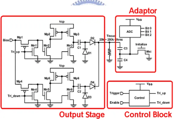
The proposed stimulus driver consists of output stage with block-capacitors, voltage-mode adaptor, and control block, as shown in Fig. 3.4. In practice, depending on different kind of stimulus sites, therapeutic requirement, and implanted time, tissue impedance varies from tens of kΩ to hundreds of kΩ. The experimental required stimulus current is 40 μA in this work. The effective impedance varies from 20 kΩ to 200 kΩ. That is to say, output voltage and required power supply are much higher than operating voltage (VDD) that in common use. And it is obvious that variation of
required operating voltage (Vcp) of output stage depends on tissue impedance correspondingly. Thus, output stage of stimulus driver adopts 0.35-μm 3.3-V/24-V BCD process which is able to tolerate 24 V at most; therefore, the proposed stimulus driver won’t suffer from problems such as gate-oxide reliability and hot-carrier degradation that might lead to failure of implantable stimulus driver. In order to reduce size of the device and power consumption, the voltage-mode adaptor and the control block adopt the 3.3-V devices with fixed operating voltage (VDD).
For safety consideration, the use of blocking-capacitors in series with the output stage of stimulus driver serves an important purpose: to prevent prolonged DC current
from flowing into the tissue in the event of semiconductor failure [36]. The current passes through the blocking-capacitors can be explained by Eq. (3-1).
Istim = C * dV / dt (3-1)
However, in order to correspond to requirement of stimulation which includes stimulus duration and amplitude of stimulus current, the size of blocking-capacitors are too large to integrate into a chip. For example, for stimulation with current amplitude of 100 μA during 1 ms, minimum capacitance requires at least 0.1 μF with 1 V voltage-drop.
Fig. 3.4. The proposed stimulus driver consists of output stage with block-capacitors, voltage-mode adaptor, and control block.
In order to resolve problem of blocking-capacitors, a number of circuit design have been studied. High-frequency current-switching (HFCS) blocking-capacitors are
utilized to reduce size of blocking-capacitors [28]. For a given stimulus current (Istim),
both reduction of pulse width (dt) or increase of voltage drop (dV) across the blocking-capacitors can lessen required size of capacitor. HFCS capacitors utilize two complementary current sources with blocking-capacitors and turn on current sources out-of-phase. Complementary stimulus current outputs (Isource1 and Isource2) converge and form a complete stimulus current (Istim) as shown in Fig. 3.5. Thus, each stimulus period is reducing, while current amplitude is unchanging, reduction ratio of blocking-capacitors is directly proportional to switching frequency. That is to say, as above example, by adopting HFCS and delivering stimulus current of 100 nS each, only 10 pF capacitor is required while the same voltage drop across blocking-capacitors. Istim Isource1 Isource2 1 ms 100 µA 100 µA 100 µA
Fig. 3.5. Complementary stimulus current outputs (Isource1 and Isource2) converge and form a complete stimulus current (Istim).
For the purpose of reducing size of blocking-capacitors and minimizing voltage drop on blocking-capacitors, switching frequency is set up at high frequency, 2.5
MHz. As shown in Fig. 3.4, output stage of the proposed stimulus driver adopts HFCS, during the stimulus driver “turn-on” interval, the control signal of Trigger, Tri_up, and Tri_down switch complementary. During upper stimulating phase, Tri_up is low (0 V) and Tri_down is high (3.3 V). For upper current source, Mn2 is biased through Mp1, and Mn3 is switched-off. The stimulus current is delivered by current mirror Mp2 and Mp3, and passes through C1 and D2. Meanwhile, down current source is discharging phase, Mn5 is switched-off, and Mn6 is switched-on. The charged C2 can discharge by D3, C2, and Mn6.
During down stimulating phase, Tri_up is high and Tri_down is low. For upper current source is discharging phase, Mn2 is switched-off, and Mn3 is switch-on. The charged C1 can discharge by D1, C1, and Mn3. Meanwhile, down current source is stimulating phase, stimulus current is delivered by current mirror Mp5 and Mp6, and passes through C2 and D4. During the stimulus driver “turn-off” interval, both Tri_up and Tri_down are high (3.3 V), gate of Mn2 and Mn5 are grounded, no stimulus current is delivered. According to structure of the proposed stimulus driver, equation of the operating voltage (Vcp) that output stage required is shown by Eq. (3-2).
Vcp = VDSp + ΔVC + ΔVDiode + RTissue Istim (3-2)
where VDSp denotes the voltage between drain and source terminals of Mp3 or Mp6,
ΔVC denotes the voltage of C1 or C2, and ΔVDiode is the voltage of D2 or D4. It is
obvious that Vcp depends on tissue impedance (RTissue) and stimulus current (RTissue). In addition, the last item of Eq. (3-2) usually dominates the required Vcp. Thus, if tissue impedance varies by factors mentioned above such as implanted time, the required Vcp changes largely, too.
site of right-side Zona Incerta (ZI) of Long-Evans rats is shown in Fig. 3.6 [37]. A 4-microwire bundle, each made of Teflon-insulated stainless steel microwires, was used to stimulate the right-side ZI (posterior 4.0 mm, lateral 2.5 mm, and depth 6.7-7.2 mm). A ground electrode was implanted 2 mm caudal to the lambda. After two hours current stimulation test, the tissue impedance between arbitrarily two microwires varies from 50 kΩ to 170 kΩ.
Fig. 3.6. Tissue impedance of experiment results verses implanted time in different stimulus site (ZI) [37].
Under the condition that required seizure suppressing stimulus current is 40 μA, the difference of varying required operating voltage is 4 V. Conventional stimulus devices are used to set the operating voltage at highest requirement and enlarge voltage compliance as large as possible [31]; however, it enlarges power consumption in great amount. The tissue impedance of specification of proposed design ranges from 25 kΩ to 200 kΩ. While tissue impedance is varying with fixed stimulus current, output
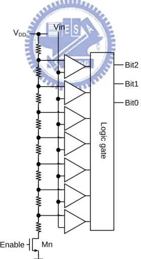
voltage is changing correspondingly. Assuming headroom of stimulus driver is 1 V, the highest required operating voltage is 9 V. By detecting tissue impedance by 1-bit ADC, stimulus driver is able to provide two levels operating voltage, 5 V while tissue impedance ranges from 25 kΩ to 100 kΩ and 9V while tissue impedance ranges from 100 kΩ to 200 kΩ; therefore, power consumption of stimulus driver is 78% of conventional works. While stimulus driver adopts 2-bit ADC, the power consumption is 66% of conventional works. While stimulus driver adopts 3-bit ADC, the power consumption is 61%. Power consumption is fewer while tissue impedance is classified into more sub-groups; however, bit number of ADC is proportional to chip area and power consumption of ADC. Thus, this work adopts 3-bit ADC with consideration of chip area and power consumption. Voltage-mode adaptor as illustrated in Fig. 3.7 is used to detect output voltage every cycle of stimulation and classifies tissue impedance into 8 sub-groups. Thus, stimulus driver can adjust Vcp for each group of tissue impedance in the most power-saving way. Voltage-mode adaptor that composes of a voltage capacitance divider and a 3-bit ADC as shown in Fig. 3.8, the adapter adopts 3.3-V devices for saving chips area.
Fig. 3.7 The voltage-mode adaptor is used to detect output voltage every cycle of stimulation and classifies tissue impedance into 8 sub-groups.
L o g ic g a te Enable Vin Bit2 Bit1 Bit0 VDD Mn
Fig. 3.8. The 3-bit ADC of voltage-mode adaptor is used to detect the voltage at output electrode.
The 3-bit ADC of adaptor adopts comparator as shown in Fig. 3.9 [38]. The comparator without DC current no matter in compare phase or hold phase is power-saving. For the purpose of converting output voltage larger than VDD (3.3 V)
into digital code, the capacitance divider is used to scale down the voltage of output stage. In accordance with product of the largest tissue impedance of 200 kΩ and stimulus current of 40 μA, the maximum convertible output voltage is 8 V, and it can be scaled down to 3.3 V by voltage divider. The relationship between input and output of capacitance voltage divider can be shown as Eq. (3-3)
Vout = Vin C3 * (C3 / C4) (3-3)
The capacitance of C3 is 1 pF, and capacitance of C4 is 1.42 pF.
Fig. 3.9. The comparator of 3-bit ADC of voltage-mode adaptor which without DC current no matter in compare phase or hold phase [37].
The Vcp is conditioned in accordance with digital output of 3-bit ADC of voltage-mode adaptor. “111” indicates the highest output voltage results from fixed stimulus current and the highest tissue impedance of specification, the highest Vcp is given. “000” indicates the lowest output voltage, the lowest Vcp is given. Assuming headroom of current source of stimulus driver is 1 V, operating voltage of conventional design and Vcp of proposed driver verses tissue impedance and corresponding digital code is shown in Fig. 3.10. While stimulation is requested, stimulus driver presets Vcp at the highest operating voltage, and delivers the first stimulus pulse. Therefore, output voltage and tissue impedance is known, according to digital output of adaptor. Namely, variety of tissue impedance is monitered. The stimulus driver can adjust Vcp before next stimulus pulse. The new proposed stimulus driver is provided with variable operating voltage, and is more power efficient.
The proposed single-phase stimulus driver to suppress epileptic seizure with
111
110
101
Conventional works
010
001
000
100
The proposed circuit
011
Fig. 3.10. Assuming headroom of current source of stimulus driver is 1 V, operating voltage of conventional design and Vcp of proposed driver verses tissue impedance and corresponding digital code.
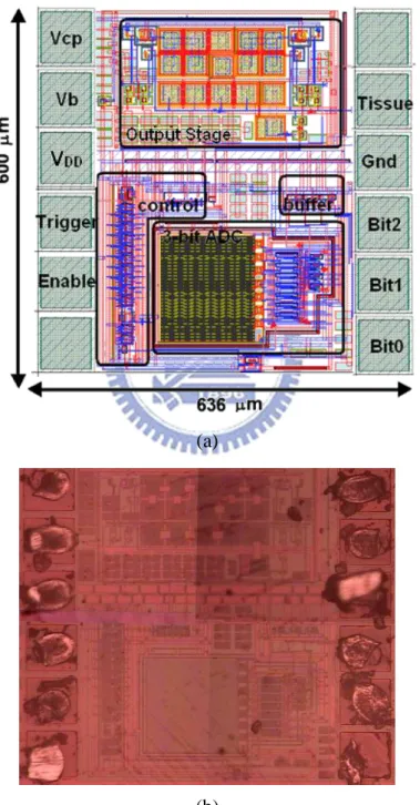
voltage-mode adaptive loading consideration has been fabricated in 0.35-μm 3.3-V/24-V BCD process. Fig. 3.11(a) and Fig 3.11(b) show the layout and chip photo of the new proposed stimulus driver. The chip size of the proposed stimulus driver is 600 636 m2.
(a)
(b)
Fig. 3.11. (a) Layout and (b) chip photo of the new proposed stimulus driver with voltage-mode adaptor.
3.3.2 Simulation Results
According to experimental demand, the stimulus current which is able to suppress epileptic seizures ranges from 20 μA to 50 μA. The output current of this stimulus driver is set by 40 μA. In addition, by experience of animal experiment, stimulus current with 800 Hz and 40 % duty cycle is efficient to regulate the abnormal discharge. Whenever epileptic seizure monitoring and controlling system detect epileptiform activity, stimulus driver deliver the specified current that mentioned above for 0.5 S.
Fig. 3.12. The simulation result of proposed stimulus driver while tissue impedance is 200 kΩ. The feedback voltage from voltage-mode adaptor is 3.2 V and digital output of 3-bit ADC is “111” which indicates the operating voltage is 12 V for tissue impedance of 200 kΩ.
Fig. 3.13. The simulation result of proposed stimulus driver while tissue impedance is 125 kΩ. The feedback voltage from voltage-mode adaptor is 2 V and digital output of 3-bit ADC is “100” which indicates the operating voltage is 9 V for tissue impedance of 125 kΩ.
Tissue impedance is classified into 8 groups by voltage-mode adaptor, each group is provided with different Vcp that is sufficient to match the minimum demand of operating voltage which describes in Eq. (3-2). Fig. 3.12 is simulation result of proposed stimulus driver, while tissue impedance is 200 kΩ
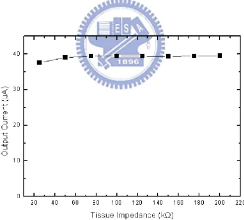
impedance of this design, output current is slightly fewer than 40 μA, 39.47 μA, with a acceptable deviation. Output voltage on stimulus site is 7.89 V, capacitance voltage divider shrinks this voltage to 3.25 V that is convertible by 3-bit ADC adopts 3.3-V device. The digital code of adaptor is “111” which indicates the highest Vcp is required. Under the condition that the largest tissue impedance is connected, the Vcp of proposed stimulus device requires at least 12 V in interval from 175 kΩ to 200 kΩ. Fig. 3.13 is another simulation result of proposed stimulus driver, while tissue impedance is 125 kΩ current is 39.4 μA. The highest Vcp, 12 V, is applied, whereas the digital code of adaptor is “100” which indicates the matching
operating voltage is 9V in interval from 100 kΩ to 125 kΩ. Thus, stimulus driver can selects lower Vcp with the same stimulus current and but lower power consumption. For example, according to the experimental results that detected impedance of rats’ brain, as shown in Fig. 3.6, it revealed that tissue fields different outcome, 50 kΩ and 150 kΩ Thus, the proposed circuit depends on their impedance and provides these stimulus site with the same stimulus current but different operating voltage. The stimulus current, required Vcp with corresponding digital code, and power consumption are shown in Fig. 3.14, Fig. 3.15, and Fig. 3.16. Required Vcp as well as power consumption depends on tissue impedance linearly, it is obvious that power consumption is fewer than using the highest requirement for any tissue impedance.
Fig. 3.15. The operating voltage (Vcp) and corresponding digital code verses tissue impedance varies from 25 kΩ to 200 kΩ.
Fig. 3.16. The power consumption verses tissue impedance varies from 25 kΩ to 200 kΩ.
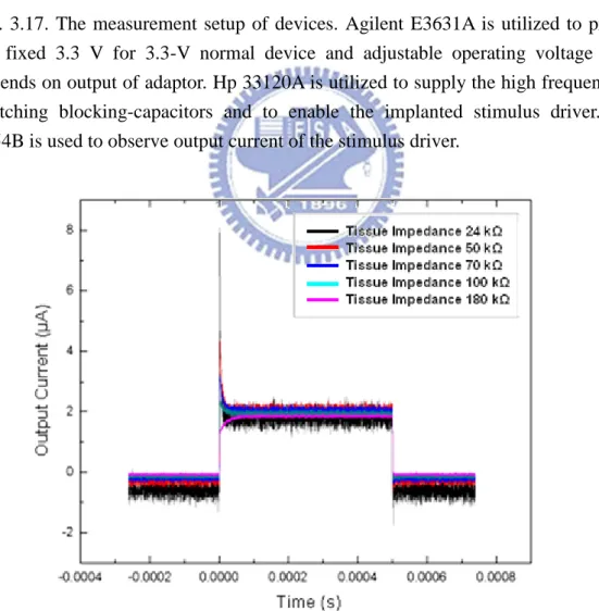
3.3.3 Measurement Results
The measurement setup of devices is shown in Fig. 3.17, where Agilent E3631A is utilized to provide the fixed 3.3 V for 3.3-V normal device and adjustable operating voltage (Vcp) depends on output of adaptor. Hp 33120A is utilized to supply the high frequency for switching blocking-capacitors and to enable the implanted stimulus driver. TDS 3054B is used to observe output current of the stimulus driver. By the original setting, voltage amplitude of all of control block and adaptor is 3.3 V and voltage amplitude of Vcp depends on digital code by adaptor, the range of Vcp from 6 V to 12 V. Fig. 3.18 shows the measurement results with original setting, which Vcp is 12 V that is highest required operating voltage; however, the output stimulus current is much smaller than expected. The output current of stimulus driver maintains 2 μA approximately while tissue impedance varies from 24 kΩ to 180 kΩ. It is too small to suppress the abnormal discharge in brain. Consequently, in order to enlarge the insufficient output current of the stimulus driver, Vcp is adjusted to 15 V which slightly higher than original setting; however, the output current still maintains 4 μA constantly as shown in Fig. 3.19.
After investigation of problems of measurement results, the reason of different outcome between simulation results and measurement results contributes to variation of nLDMOS. The discharging nLDMOS of Fig. 3.20, Mn3 and Mn6, are primary cause. The output stage of stimulus driver adopts blocking-capacitors that obstacle DC current flow. By complementary stimulating phase and discharging phase, integrated stimulus current is able to flow through series-connected blocking-capacitors. Once stimulus current pass through blocking-capacitors and stimulate tissue on site, charge accumulate on one side of blocking-capacitors and cause potential difference.
Fig. 3.17. The measurement setup of devices. Agilent E3631A is utilized to provide the fixed 3.3 V for 3.3-V normal device and adjustable operating voltage (Vcp) depends on output of adaptor. Hp 33120A is utilized to supply the high frequency for switching blocking-capacitors and to enable the implanted stimulus driver. TDS 3054B is used to observe output current of the stimulus driver.
Fig. 3.18. The measurement results with original setting, which Vcp is 12 V that is highest required operating voltage (Vcp). The output current of stimulus driver maintains 2 μA approximately while tissue impedance varies from 24 kΩ to 180 kΩ.
Fig. 3.19. Vcp is adjusted to 15 V which slightly higher than original setting; however, the output current still maintains around 3 μA.
Fig. 3.20. The discharging nLDMOS, Mn3 and Mn6, are primary cause. The
accumulated charge can not discharge from discharging nLDMOS. After first stimulus pulse of each stimulus current source, the blocking-capacitors, C1 and C2, are
During discharge phase, the accumulated charge on blocking-capacitors discharge by discharging nLDMOS, Mn3 and Mn6, and potential difference is eliminated. However, nLDMOS that are used to discharge the accumulated charge can not fully switch on during discharge phase with control signal of 3.3 V, that results in the accumulated charge can not pass through discharging nLDMOS and potential difference still exist across blocking-capacitors, blocking-capacitors are saturated. Thus, in next stimulating phase, the saturated blocking-capacitors are unable to transmit stimulus current by yielding further potential difference and result in the failure as mentioned above. By Fig. 3.17 and Fig. 3.18, the failure which is caused by discharging nLDMOS can be recognized perspicuously. At the beginning of stimulation, blocking-capacitors of two current sources of output stage are not saturated; each current source is able to deliver stimulus current correctly at first stimulating phase and creates a current spike that much stronger than rest period of stimulation. After first stimulating phase, blocking-capacitors are unable to discharge correctly at corresponding discharging phase. Therefore, during next stimulating phase, output of stimulus driver is much fewer than expected.
According to result of investigation, this failure ascribes to variation of threshold voltage of nLDMOS. Operating voltage VDD of 3.3-V device is adjusted for the
purpose of switching on the discharging nLDMOS. While supply voltage of 3.3-V device is adjusted to 6 V, the current output of stimulus driver increase dramatically and reach up to 30 μA which corresponds to cooperative experimental requirement. Fig. 3.21 shows measured current output of stimulus driver maintains 30 μA while tissue impedance of 24 kΩ and 200 kΩ. The practical tissue impedance varies randomly from tens of kΩ to hundreds of kΩ, the measured results of the output current from 24 kΩ to 200 kΩ are shown in Fig. 3.22, and corresponding Vcp is shown in Fig. 3.23. The deviation of stimulus current between measurement results
and simulation results is 75%.
In accordance with original setting, stimulus current of 40 μA and tissue impedance ranges from 24 kΩ and 200 kΩ, tissue impedance is classified into 8 sub-groups by voltage-mode adaptor. However, the measured current output is 30 μA, the maximum voltage on output is 6 V. That is to say, voltage-mode adaptor can classifies tissue impedance into 6 sub-groups and provides suitable Vcp. Due to adjustment of operating voltage for 3.3-V device and 0.35-μm 3.3-V/24-V BCD device, power consumption is higher than expected. The operating voltage Vcp of 3.3-V/24-V device is set from 12.2 V to 22 V, and the average power consumption is 0.385 mW.
Fig. 3.21. While supply voltage of 3.3-V device is adjusted to 6 V, the current output of stimulus driver increases dramatically and reaches up to 30 μA while tissue impedance is within 24 kΩ and 200 kΩ.
Fig. 3.22. The measurement results of the output currents as VDD is adjusted to 6 V.
Fig. 3.23. The measurement results of the corresponding operating voltage from 24 kΩ to 200 kΩ.
3.3.4 Integration of the Proposed Single-Phase Stimulus Driver and Epileptic Seizure Monitoring and Controlling System
The prototype of proposed stimulus driver has been integrated into closed-loop epileptic seizure monitoring and controlling system which is conducted by National Cheng-Kung University. Long-evens rats, aged 4-6 months and weighting 500-700 g, are selected for experiment in this study. All surgical and experimental procedures were reviewed and approved by Institutional Animal Care and Use Committee of National Cheng-Kung University. The rats were anesthetized with sodium pentobarbital (50 mg/kg, i.p.).
The closed-loop epileptic seizure monitoring and controlling system consists of microcontroller, data acquisition, wireless transceiver, host computer [26]. By analyzing brain activities of Long-evens rats which suffer from spontaneous absence seizures and epileptiform activities induced by pentylenetetrazol (PTZ), the system can detects epileptic seizure simultaneously and stimulates the right-side zona incerta (ZI) (posterior 4.0 mm, lateral 2.5 mm, and depth 6.7-7.2 mm). Stimulus current is conducted by a 4-microwire bundle, each made of Teflon-insulted stainless steel wire while ground electrode was implanted 2 mm caudal to lambda.
Measurement setup of integration experiment of proposed stimulus driver and closed-loop epileptic seizure monitoring and controlling system are shown in Fig. 3.24 and Fig. 3.25. As monitor of the system shown, brain activity is clearly detected and recorded. Whenever the system detects an epileptic seizure, the proposed stimulus driver is given a stimulation signal and stimulates ZI. Duration of stimulation is 0.5 s. As the measurement results as mentioned above, the setting of the proposed stimulus driver depends on tissue impedance of Long-evens rats, the tissue impedance is 150 kΩ and operating voltage Vcp for HV-device is 18 V, correspondingly.
Fig. 3.24. The measurement setup of integration experiment of proposed stimulus driver and closed-loop epileptic seizure monitoring and controlling system.
Fig. 3.25. The measurement setup of integration experiment of proposed stimulus driver and closed-loop epileptic seizure monitoring and controlling system.
Fig. 3.26. The experiment result without injection of PTZ, epilepsy seizure with abnormal discharge was detected at the second sec, and the system triggered the proposed stimulus driver to stimulate ZI. After once stimulation, the intensive and rapidly brain activity was suppressed.
Two experiments, without injection of PTZ and with injection of PTZ, have been conducted and each of experiments is conducted for 10 minutes. Fig. 3.26 is a one of the experiment result which without injection of PTZ, epilepsy seizure with abnormal discharge was detected at the second sec, and the system triggered the proposed stimulus driver to stimulate ZI. After once stimulation, the intensive and rapidly brain activity was suppressed. Fig. 3.27 is an experiment result which with injection of PTZ, abnormal brain activity was much severe. The system detected the first seizure and stimulated; however, epileptic seizure wasn’t been suppressed, first stimulation was invalid. Thus, abnormal brain activity was still detected by the system; second stimulation was given and was effective to suppress epileptic seizure. Because this experiment was conducted with injection of PTZ, epileptiform activity was induced and became unstable. The second seizure just happened after suppression of the first
seizure, and was suppressed by stimulation immediately. According to experiment results, integration of closed-loop epileptic seizure monitoring and controlling system and prototype of the proposed stimulus driver have been verified.
Fig. 3.27. The experiment result with injection of PTZ. The system detected the first seizure and stimulated; however, epileptic seizure wasn’t been suppressed. Thus, abnormal brain activity was still detected by the system; second stimulation was given. With injection of PTZ, epileptiform activity became unstable. The second seizure happened after suppression of the first seizure, and was suppressed by stimulation.
3.4 Summary
Design of single-phase stimulus driver to suppress epileptic seizure with voltage-mode adaptive loading consideration is investigated and verified in this chapter. While tissue impedance varies from tens of kΩ to hundreds of kΩ, the proposed stimulus driver utilizes 0.35-μm 3.3-V/24-V BCD process to prevent
problems of reliability and voltage overstress. In addition, the proposed stimulus driver with voltage-mode adaptor which is used to classify tissue impedance is provided with adjustable operating voltage. Even if unexpected variation of nLDMOS affects the measured setting, the measurement results still demonstrate that operation with stair-like operating voltage which designates by voltage-mode adaptor is workable. Comparison of conventional works with fixed operating voltage, the advantage of this work is adaptive against variation of tissue impedance. Furthermore, the prototype of the proposed stimulus driver has been integrated into closed-loop epileptic seizure monitoring and controlling system, results of animal experiment show that integration of the proposed stimulus driver and the system is feasible and compatible.
Chapter 4
Design of Bi-Phase Stimulus Driver to Suppress
Epileptic Seizure with Current-Mode Adaptive
Loading Consideration
4.1 Introduction
With the consideration of reliability and power consumption, the stimulus driver used in the implantable device for epileptic seizures control is investigated in this work. The required stimulus current ranges from 20 μA to 50 μA in cooperative experiment. The effective impedance of electrode varies from 25 kΩ to 200 kΩ because of different kind of tissue, location, and implanted time. In order to meet the requirements, output voltage range of stimulator should be designed from 0.5 V to 10 V, that higher than operating voltage in common used. Therefore, the 0.35-μm 3.3-V/24-V BCD process is utilized in this work for the stimulus driver and chip implementation. Power consumption is also the critical consideration, because it is inversely proportional to the use time in implantable device. In order to minimize power consumption of this stimulator, supply voltage of this work can be adjusted according to different impedance by current-mode adaptor.
To integrate with implantable epileptic seizure monitoring and controlling system, the high operating voltage for 24-V device should been generated by stimulus driver itself while rest of the system utilize the same operating voltage (VDD). Therefore,
charge pump circuit is an indispensible part of the stimulus driver. This work, charge pump has been integrated into this proposed stimulus driver. In addition, as common
![Fig. 2.3. The electrode array which is used for long-term EEG recording [18].](https://thumb-ap.123doks.com/thumbv2/9libinfo/8226908.170771/21.892.202.707.180.562/fig-electrode-array-used-long-term-eeg-recording.webp)
![Fig. 2.4. Vagus nerve stimulation [20].](https://thumb-ap.123doks.com/thumbv2/9libinfo/8226908.170771/22.892.205.701.124.835/fig-vagus-nerve-stimulation.webp)
![Fig. 3.6. Tissue impedance of experiment results verses implanted time in different stimulus site (ZI) [37]](https://thumb-ap.123doks.com/thumbv2/9libinfo/8226908.170771/36.892.219.693.411.793/tissue-impedance-experiment-results-verses-implanted-different-stimulus.webp)
![Fig. 3.9. The comparator of 3-bit ADC of voltage-mode adaptor which without DC current no matter in compare phase or hold phase [37]](https://thumb-ap.123doks.com/thumbv2/9libinfo/8226908.170771/39.892.217.663.539.1007/comparator-voltage-adaptor-current-matter-compare-phase-phase.webp)