2170 IEEE JOURNAL OF SOLID-STATE CIRCUITS, VOL. 48, NO. 9, SEPTEMBER 2013
A 81-dB Dynamic Range 16-MHz Bandwidth
Modulator Using Background Calibration
Su-Hao Wu, Student Member, IEEE, and Jieh-Tsorng Wu, Senior Member, IEEE
Abstract—A fourth-order discrete-time delta-sigma modulator
(DSM) was fabricated using a 65-nm CMOS technology. It com-bines low-complexity circuits and digital calibrations to achieve high speed and high performance. The DSM is a cascade of two second-order loops. It has a sampling rate of 1.1 GHz and an input bandwidth of 16.67 MHz with an oversampling ratio of 33. It uses high-speed opamps with a dc gain of only 10. Two different types of digital calibrations are used. We first employ the integrator leakage calibration to correct the poles of the integrators. We then apply the noise leakage calibration to minimize the leaking quantiza-tion noise from the first loop. The noise leakage calibraquantiza-tion also relaxes the component-matching requirements. Both calibrations can operate in the background without interrupting the normal DSM operation. The chip’s measured signal-to-noise-and-distor-tion ratio and dynamic range are 74.32 and 81 dB, respectively. The chip consumes 94 mW from a 1 –V supply. The active area is
0.33 0.58 mm .
Index Terms—Analog–digital conversion, analog-to-digital
con-verter (ADC), calibration, delta-sigma modulation, oversampling, switched-capacitor circuits.
I. INTRODUCTION
T
HE delta-sigma modulator (DSM) is an analog-to-digital conversion technique that uses oversampling and noise shaping to enhance the conversion resolution. Compared with Nyquist-rate ADCs that offer similar input signal bandwidth, the DSMs operate at a much higher circuit speed. The performance of a wide-band discrete-time (DT) DSM is usually limited by its internal opamps that realize the integrator function. For an input bandwidth of 20 MHz and an over-sampling ratio (OSR) of 32, the corresponding sampling rate is , and the re-quired opamp unity-gain frequency is about . It is difficult for an opamp with such a speed to have a de-cent dc gain. Circuit-level gain enhancement techniques, such as multiple-stage configuration [1], correlated double sampling [2], and correlated level shifting [3], all sacrifice the speed.In a DT DSM, an integrator realized with a low-gain opamp loses some of its ability to suppress in-band quantization noises. The integrator transfer function is also more sensitive to process-voltage-temperature (PVT) variations. The dc gain requirement for the opamps can be relaxed by increasing Manuscript received January 17, 2013; revised May 06, 2013; accepted May 07, 2013. Date of publication June 05, 2013; date of current version August 21, 2013. This work was supported by the National Science Council of Taiwan under GrantNSC-101-2221-E-009-161. This paper was approved by Associate Editor Ichiro Fujimori.
The authors are with the Department of Electronics Engineering and Institute of Electronics, National Chiao Tung University, Hsin-Chu 300, Taiwan (e-mail: [email protected]).
Color versions of one or more of the figures in this paper are available online at http://ieeexplore.ieee.org.
Digital Object Identifier 10.1109/JSSC.2013.2264137
the order of the DSM loop, or by employing the multi-stage noise-shaping (MASH) structure [4]–[7]. A higher-order DSM may require more quantization levels from its internal analog-to-digital converter (ADC) and digital-to-analog (DAC) to stabilize the loop [8], yielding complex circuits. On the other hand, the MASH modulators may require calibration to correct the effects of component mismatches and integrator variations [9], [10]. There is an alternative MASH structure that can mitigate the matching requirements [11].
This paper describes a DT DSM that combines low-com-plexity circuits and digital calibration to achieve wide band-width and large dynamic range. It is a MASH modulator con-sisting of two cascaded second-order loops. The number of the quantization levels of its internal ADCs and DACs is only 4. The internal integrators are realized with high-speed opamps with a dc gain of only 10. Two different types of digital cal-ibrations are applied. We first employ the integrator leakage calibration to correct the poles of the integrators. We then use the noise leakage calibration to minimize the quantization noise from the first loop leaking to the DSM combined output. The noise leakage calibration also relaxes the component matching requirements for the MASH structure. Since each calibration ad-justs only one parameter, it is robust. All calibration can proceed in the background without interrupting the normal DSM opera-tion. The calibration processors are simple digital circuits. They do not include any complex filter. The modulator was fabricated using a 65 nm CMOS technology. It has a sampling rate of 1.1 GHz and an input bandwidth of 16.67 MHz with an oversam-pling ratio (OSR) of 33. The measured signal-to-noise-and-dis-tortion ratio (SNDR) and dynamic range (DR) are 74.32 and 81 dB, respectively. The chip consumes 94 mW from a 1-V supply. The active area is 0.33 0.58 mm .
The remainder of this paper is organized as follows. Section II describes the DSM architecture and its design parameters. Section III describes the integrator leakage cali-bration and its design consideration. Section IV describes the noise leakage calibration. Section V describes the design of the crucial circuits. Section VI shows the experimental results. Section VII draws conclusions. In addition, Appendices A and B analyze the transient behavior and the fluctuation of the integrator leakage calibration, respectively.
II. DSM ARCHITECTURE
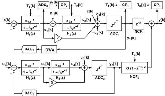
Fig. 1 shows the reported fourth-order DT DSM architecture. In its core is a MASH modulator consisting of two stages of second-order modulation loops. There are four integrators, to . Each integrator is modeled with a gain factor and a pole . Table I shows the design values for and . For an ideal integrator with an opamp dc gain , . 0018-9200 © 2013 IEEE
Fig. 1. Fourth-order MASH DSM with digital calibrations.
TABLE I
INTEGRATOR VARIATIONS DUE TO OPAMP DC GAIN
There are two ADCs (digitizers), and . Each one is a 2-bit flash ADC comprising three comparators. There are
two corresponding DACs, and . covers an
output range of , while covers an output range of . The adders preceding the two ADCs are passive switched-capacitor circuits. In the first loop, a data-weighted averaging (DWA) dynamic element matching logic [12] is added before to mitigate its conversion errors. A full-scale sine-wave input is defined as , which has a
signal power of . In our design, 1 V. The
use of multibit ADCs leads to smaller quantization errors and stability improvement. The combination of filter feedforward and multibit ADCs relaxes the linearity and voltage swing requirements for the analog circuitry [13].
As shown in Fig. 1, the raw digital outputs from the two mod-ulation loops are and , respectively. Due to the use of feed-forward, both loops have a signal transfer function (STF) of 1,
i.e., and . The two
digitizers and introduce quantization noises, de-noted as and , respectively. The two noise transfer
func-tions are defined as and .
is a function of and , while is a function of and . Applying the and parameters listed in Table I with an opamp dc gain , the resulting noise transfer functions are
and . Two digital noise-cancellation filters and combine the two outputs and to gen-erate the final DSM output , which can be expressed as
(1)
where the noise leakage transfer function NLF is defined as (2) If we choose the digital filters and
with , then, in the DSM
combined output , is completely eliminated, and is shaped by a fourth-order function .
In the wide-bandwidth applications, the DSM uses high-speed opamps to implement the integrators. In our design, the opamps in the integrator configuration have a unity frequency of 6 GHz, but have a dc gain of only 10. Table I shows the effect of on the integrators. Their gain factors change and their poles become less than 1. When placing these integrators in the DSM, the corresponding NTF exhibits a degraded capability of suppressing quantization noise in the signal band. Besides the effect on and , the capacitor mismatch in an integrator also causes a change in . Both the and the variations yield . This phenomenon is called noise leakage, when a portion of leaks out to the DSM output .
Fig. 2 shows the effect of on the noises and appearing in the output . It plots the ratio of noise power to the signal power of a full-scale sine-wave input, . The noise power includes only the frequency components within the signal band. An OSR of 33 is assumed. is the noise power of in and is the noise power of in . It is assumed that all integrators have the same . In our design, is a weak function of . It can be neglected if the expected signal-to-noise ratio (SNR) of the entire DSM is 80 dB. On the other hand, is a strong function of . It requires , so that is 85 dB below .
From (1) and (2), and since is a simple delay, the digital filter must match the analog integrators and to reduce . The filter can become adaptive to accommodate the variations in and [14]. However, if the parameters in and are away from 1, the calibration
2172 IEEE JOURNAL OF SOLID-STATE CIRCUITS, VOL. 48, NO. 9, SEPTEMBER 2013
Fig. 2. Effect of integrator pole on the noises and in the DSM output.
for are complex. In our design, we first calibrate integra-tors and to simplify the requirement for . We then calibrate to minimize the NLF of (2). We apply the inte-grator leakage calibration described in Section III to inteinte-grators and to recover their capability of noise suppression and make their approximate 1. We simplify the second
noise-can-cellation filter as , which has only one
adaptive parameter . We then apply the noise leakage calibra-tion described in Seccalibra-tion IV to find . All calibracalibra-tions are op-erated in the background without interrupting the normal DSM function.
The quantization noise may contain harmonic tones or idle tones. These tones may show up in the signal band of the DSM output . Furthermore, these tones may correlate with the calibration signals introduced by the aforementioned calibra-tions, corrupting the calibration process. Therefore, as shown in Fig. 1, a dithering signal is added to the input of to randomize . This dithering signal is taken from the output of the integrator , which is the quantization noise with first-order noise shaping. The dithering signal is not included in the following analyses since its effect is minuscule.
III. INTEGRATORLEAKAGECALIBRATION
The reported DSM includes four switched-capacitor (SC) in-tegrators. Each SC integrator contains an opamp. Neglecting its settling behavior, the integrator transfer function is
. If the dc gain of the opamp is finite, then , and the integrator becomes lossy. If the input of this in-tegrator is 0, then its output can then be expressed as
. Its output loses an amount of for every clock cycle. The issue is known as integrator leakage.
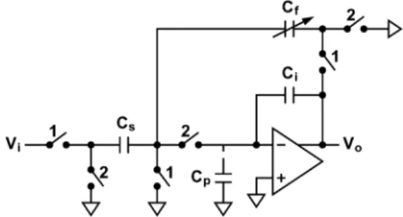
Fig. 3 shows the integrator with leakage compensation. It is driven by two nonoverlapping clocks and . The switches labeled with 1 are turned on when . The switches la-beled with 2 are turned on when . The circuit is a con-ventional noninverting integrator with an additional positive feedback for leakage compensation [15]. The capacitor puts back amount of charge into for every clock cycle. The
of the integrator becomes
(3)
Fig. 3. Integrator with leakage compensation.
where is the opamp dc gain, and is the parasitic capaci-tance at the opamp input. To obtain a lossless integrator, we want so that . Comparing with is rel-atively small. The capacitor itself and its associated switches add minuscule loading and noise to the integrator. Since the op-timal value for depends on voltage gain , which is sen-sitive to PVT variations. The capacitor is automatically ad-justed by the calibration described below.
As shown in Fig. 1, the integrator leakage calibration is ap-plied to the integrators and of the first modulation loop. Consider the calibration of the first integrator . The ca-pacitor in is controlled by a digital signal such that
(4) where is an integer, is the digital control step size and is the capacitance when . From (3), the corresponding of is approximated by
(5)
where . The control signal is generated
from a calibration processor, . To calibrate , a calibration signal is added to the input of the second integrator . receives the output , and detects the of from the
-related signal embedded in . It then adjusts to make approximate 1.
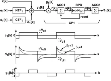
Fig. 4 shows the block diagram and its input compo-nents. At the input, the digital stream is a summa-tion of (1) the input , (2) the quantization noise shaped by the noise transfer function , and (3) the calibra-tion signal shaped by the calibration-signal transfer function , which is defined as . The calibration signal is a square wave with frequency, amplitude, and 50% duty cycle. The square wave excites , yielding . Thus, embedded in is the step response of trig-gered by . This step response settles toward a final value of
(6) shows the same polarity as . Thus, can deter-mine if is above or below 1 by detecting the polarity of . As shown in Fig. 4, extracts the information from by correlating with a triple-valued sequence . This waveform has the same polarity as , but its value is set to 0 during the initial transition phase of . The resulting signal sequence is accumulated on an
Fig. 4. Calibration of integrator .
Fig. 5. AAR operation.
accumulator ACC1 followed by a binary peak detector (BPD). Together they perform the accumulation-and-reset (AAR) op-eration [16]–[18] to guess the polarity of while removing the perturbations caused by and . The AAR operates as follows. The accumulator ACC1 accumulates the sequence. Its output is monitored by the BPD with a threshold . Whenever reaches either or , the BPD issues an output or for one clock cycle respectively and reset accumulator output to 0. The BPD output remains
at 0 when . The BPD output is an
estimate of the polarities of and . uses it to increase or decrease the control signal . Thus, following is another accumulator, ACC2, that accumulates the sequence. Its output controls the capacitor of the integrator , thus adjusts its . Fig. 5 illustrates the time-domain waveform of the ACC1 output , and the waveform of the resulting . When approaches 1, both and become smaller, and it takes a longer time to activate the BPD.
The above calibration scheme involves signal correlation and AAR operation. For this calibration to be effective, it requires that the calibration signal has no correlation with other sig-nals in , including the input and the quantization noise . Since is out of the signal band of , there is no correlation be-tween and . Assume is a white noise. There are frequency components in that can have correlation with . However, this correlation is weak since those frequency components have
randomly varying phases. The effect of this correlation can be overcome by choosing a large BPD threshold .
This calibration scheme has five design parameters, including the amplitude, , the frequency, , the duty ratio, , the BPD threshold, , and the control step size, . Referring to Fig. 4, the duty ratio is defined as the ratio of the time for to the time for . The
duty ratio for and is assumed to be the
same as .
As shown in Fig. 4, the calibration square wave triggers a step response . Let have a frequency of , a corre-sponding period of , and a duty cycle of 50%. We want to be larger than the signal bandwidth so that it can be removed by the decimation filter following the DSM. We also want to be longer than the time required for to settle so that its final value can be extracted by correlating
with . In our design, and , so that, in
each transient, has a period of 16 clock cycles to settle be-fore is activated for 16 clock cycles. The frequency of is . As long as , the frequency components of is outside the signal band.
The injection of increases the signal ranges of the inte-grators’ outputs, and . A larger and larger raise the nonlinearity effect of the integrators. A large may even over-load the second modulation loop, yielding large . Thus, an increase in the amplitude, , degrades the SNDR of the DSM. On the other hand, from (6), if is too small, the cor-responding is too small to ensure a robust calibration. We choose by using simulations. In the simulations, all integra-tors are assumed to have a pole at . Without the injection of , the peak SNDR of the entire DSM is 88.5 dB occurring at an input level of 0.25 dBFS. The peak SNDR is degraded by more than 6 dB if . For our design, we choose . The resulting peak SNDR is maintained at 88 dB. Without , the signal standard deviation for and are
and , respectively. When
with is injected, and become
and , respectively.
Fig. 5 illustrates the transient response of during the cali-bration. As analyzed in Appendix A, this averaged transient be-havior can be modeled as a first-order linear system. The tran-sient response of can be expressed as
(7) where the time constant is
(8) It is assumed the digitizer has an analog-to-digital con-version gain of . From (8), a smaller and a larger lead to smaller , yielding a faster calibration speed.
Fig. 5 shows that, as the calibration process converges, the behavior of becomes a discrete random fluctuation around 1. Referring to Fig. 4, both the input and the quantization noise induce this fluctuation. Their effects are diminished by the AAR operation. A larger and a smaller lead to a smaller fluctuation in , yielding the better SNDR performance for the DSM. As increases, the standard deviation of
2174 IEEE JOURNAL OF SOLID-STATE CIRCUITS, VOL. 48, NO. 9, SEPTEMBER 2013
fluctuation, , converges to an averaged value that can be expressed as [17]
(9) Appendix B contains a simplified derivation of the above equa-tion. As shown in Fig. 2, the deviation of from 1 increase the
noise power . we want so that is
85 dB below . In this design, we choose
and , yielding a time constant . If
the clock rate 1 GHz, the physical time constant
is 248.1 s.
Referring to Fig. 1, to calibrate the second integrator , a calibration square wave is added to the input of . An additional digitizer is added to convert , the output of the first integrator , into a digital stream . ADC3 is also a flash ADC, comprising three comparators with thresh-olds at . The calibration processor receives and generates to adjust the of . The control signal adjusts by controlling the capacitor in . The control mechanism is similar to (4) and (5).
The output comprises: 1) the
quantiza-tion noise ; 2) the quantization noise shaped by ; and 3) the calibration signal shaped by , where is the transfer function from to . The calibration signal is a square wave with frequency, amplitude, and 50% duty cycle. Similar to the -to- response shown in Fig. 4, triggers the step response of . This step response settles toward a final value of
(10) This is extracted by to detect the polarity . The operation of is identical to that of . It correlates with a triple-valued sequence , which has a duty ratio of . The AAR eliminates the perturbation caused by and . The AAR has a BPD threshold of . Comparing to the of (6), has an opposite polarity. Thus, comparing with the of Fig. 4, the polarity of is inverted. For our design, has a period of and an amplitude of . The duty ratio of is . The BPD threshold for the AAR is . The control step size is . The above design parameters result in
a calibration time constant of or
101.3 s with a 1-GHz clock. When the calibration signal is injected into the DSM, the signal standard deviations for and
are and , respectively.
The calibration and the calibration are executed se-quentially. They do not interfere with each other. The operations are robust. The calibration signals and are easy to generate. The calibration processors and can be realized with simple digital circuits. They use the masking signals and to extract the calibration data. Complex filter is not needed.
IV. NOISELEAKAGECALIBRATION
From (1) and (2), the quantization noise can leak into the DSM output if the noise leakage transfer function . After the integrator leakage calibration described in Section III, the of and the of are close to 1.
Fig. 6. Noise leakage calibration and calibration processor .
However, the gain factors and are still subjected to PVT variations. With and , the second noise-cancella-tion filter can be simplified as , where is a gain factor. Since , the noise leakage function for can be approximated by
(11) We want to minimize NLF. As shown in Fig. 1, the gain factor is adjusted by a digital control , such that
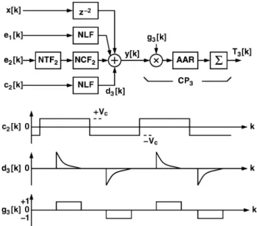
(12) where is an integer, is the control step size, and is the value of when . The control is generated from the calibration processor .
During the integrator leakage calibration of , a calibration square wave is added to the input of . Similar to the quantization noise , passes through NLF and ap-pears in the DSM combined output . Thus, can observe , extract the -related signal in , and then adjust through
to make disappear from .
Fig. 6 shows the block diagram and its input compo-nents. The DSM output contains: 1) the input delayed by the filter ; 2) the quantization noise shaped by NLF; 3) the quantization noise shaped by ; 4) the calibration signal shaped by NLF. The calibration square wave excites the NLF filter, yielding . Thus, embedded in , is the step response of NLF triggered by . As expressed in (11), the NLF filter is a filter with a time delay of two clock cycles and a gain factor of . The filter is a high-pass filter with two zeros close to dc. Thus, the time-do-main step response of NLF is a spike and settles toward zero. detects the energy of those spikes and then adjusts to eliminate the spikes. The operation of is similar to those of and . It correlates with a triple-valued sequence with a duty cycle of . The sequence is aligned with the spikes in . Its active region overlaps the major
Fig. 7. Operational amplifier schematic.
area of the spikes. The AAR in CP3 eliminates the perturbation caused by , , and . The AAR has a BPD threshold of . The output adjusts as expressed in (12). For our design, the duty ratio of is . The BPD threshold for the
AAR is . The control step size is . The
above design parameters result in a calibration time constant of or 651.4 s with a 1-GHz clock. This time constant is larger than the time constants for the inte-grator leakage calibration, and .
During the power-on phase, is reset and and . According to (11), when the calibration converges, . To reduce the initial calibration convergence time, we choose a that is close to , which can be calculated as
(13) where , , and are the capacitors in the integrator , and , , and are the capacitors in the integrator . Capacitors and are functions of control signals and respectively. The power-on sequence for calibration is described as follows. The DSM first executes the calibration for 1 ms, and then the calibration for
0.4 ms. Afterward, the DSM uses the values of and from the above calibrations to estimate and , and applies (13) to calculate . The DSM then activates CP3 every time when the calibration is in progress.
V. CIRCUITDESIGN
Here, we describe the circuit design to implement the DSM of Fig. 1. The DSM is to be fabricated using a 65-nm CMOS technology. The supply voltage is 1 V. The DSM is expected to achieve a sampling rate higher than 1 GS/s and a DR larger than 80 dB.
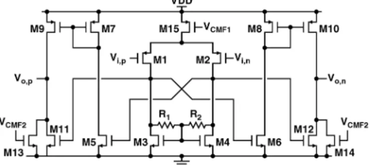
Fig. 7 shows the schematic of the opamps used in the inte-grators. It is a two-stage class-AB amplifier without frequency compensation [19]. All MOSFETs are sized with the minimum channel length of 60 nm. The amplifier has a dc voltage gain of 10. Its dominant poles are located at the output nodes and . When configured as an integrator, the opamp achieves an unity-gain frequency of 6 GHz and a phase margin of 63 de-grees. The voltages and are generated by two separate continuous-time common-mode feedback (CMFB) cir-cuits. Each CMFB contains additional voltage amplification to increase the loop gain and improve the common-mode rejection
against power-line fluctuation. The push-pull output stage also provides additional common-mode rejection.
The opamp is used to realize the fully differential version of the integrator shown in Fig. 3. The input common-mode voltage of the opamp is set to . The analog switches connected to the opamp’s inputs are nMOSFETs with boosting gate con-trol [19]. Consider the integrator . Its ideal value of the gain factor is determined by the capacitor ratio .
In our design, the thermal noise from the first integrator is the dominant source of thermal noise. Its total noise power showing up in the signal band of the DSM output is about [8]. We choose 1.9 pF so that the power of this thermal noise in the signal band, , is 90 dB below the power of a full-scale sine-wave input, . By using the periodic noise analysis of the circuit simulator, we estimate that the total of the entire DSM is 86 dB below .
The control signal adjusts the capacitor in the inte-grator as described by (4), thus varying as described by (5). The capacitor step size determines the step size .
From Section III, we want . In our
de-sign, is a 6-bit control signal, and can be varied from 0 to 378 fF with a step size 6 fF. As a result, can be varied from 0.964 to 1.028 with a step size . Similarly, the output controls the capacitor in the integrator . The signal is a 5-bit control signal, and can be varied from 0 to 186 fF with a step size 6 fF. As a result, can be varied from 0.957 to 1.027 with a step
size .
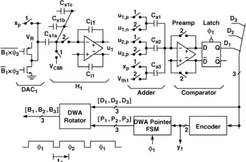
Fig. 8 shows the schematic of and the adder preceding in the first modulation loop of the DSM. Only one side of the fully-differential circuit is depicted. The adder is a passive switched-capacitor circuit [20], comprising three capacitors to . The capacitors have an identical capacitance of 60 fF. During , the preamplifier in the comparator is reset with its input shorted to its output. Meanwhile, the inverse of from the integrator , the output from the integrator , and a comparator threshold voltage are sampled onto capacitors , , and , respectively. The input offset of the pream-plifier is also stored on the capacitors. During , the output
from , the output from , and the modulator input are connected to the capacitors respectively, yielding a
differen-tial voltage at the input of the
pream-plifier. Upon the falling edge of , the latch in the comparator
compares with the threshold ,
gen-erating a single-bit digital output . There are 3 comparators in . They compare with three different thresholds, which
are , , and .
All of the integrators in this DSM sample their input during and perform the integration during . As shown in Fig. 8, the input sampling capacitor of the integrator is divided into three identical capacitors , , and to implement the 2-bit equally weighted . During , the input is sampled onto all three capacitors. During , the capacitors are connected to either or 0, depending on the three binary signals , , and , respectively. For capacitor , it is connected to if and is connected to ground
if .
The analog input of the DSM, , is sampled onto the ca-pacitor in the first integrator and the capacitor in the
2176 IEEE JOURNAL OF SOLID-STATE CIRCUITS, VOL. 48, NO. 9, SEPTEMBER 2013
Fig. 8. Schematic of the first loop in the DSM and its timing scheme.
passive adder simultaneously. The sampling switches connected to , , and are boostrapped nMOSFET switches [21]. These switches need to meet the linearity requirement the DSM. The sampling switches connected to the capacitors are regular CMOS switches. The linearity requirement of these switches are less critical.
In Fig. 8, the comparator output set is
a thermometer code. An encoder converts into a 2-bit Gray code , which serves as the output. A data-weighted-av-eraging (DWA) rotator also receives and generates the input set to mitigate the mismatches among
, , and . The rotator is a passive switch matrix con-trolled by a DWA pointer, which is a finite-state machine (FSM) [22].
In Fig. 8, the critical path is from the latch in the comparator to the first integrator . Upon the falling edge of , the latches in all three comparators begin the regeneration process to update
. The change must propagate to the switches in time so that the integrator receives the correct
output during . The duration from the falling edge that triggers the latches in the comparators to the falling edge that ends the integration operation is only half of the clock period. If the sampling frequency of the DSM is 1 GHz, half of the clock period is 500 ps. We define the propagation delay from the latch in the comparator to the switches as . It is critical to minimize so that the integrator is given enough time to settle during .
As illustrated in Fig. 8, a comparator consists of a preampli-fier followed by a latch. The preamplipreampli-fier is a two-path amplipreampli-fier that combines the high gain of a two-stage amplifier with the high-speed of a single-stage amplifier [23]. The latch is a cas-cade of a dynamic sense amplifier [24] and a static S-R latch [25]. The preamplifier has a dc gain of 22 dB. It achieves a unit-gain frequency of 16.5 GHz with a phase margin of 68 de-gree. The propagation delay defined in Fig. 8 depends on the
signal magnitude , where
is the comparator input and is the threshold of the
com-Fig. 9. Modulator chip micrograph.
TABLE II
POWER ANDAREA OFCIRCUITBLOCKS
parator. As decreases, it takes longer time for the latch to regenerate a valid output. In our design, 125 ps if 1 mV. That leaves about 300 ps for the first integrator to settle during , if the rise time, fall time, and nonoverlapping time of the clocks are taken into account.
VI. EXPERIMENTALRESULTS
The DSM shown in Fig. 1 was fabricated using a 65-nm CMOS technology. Fig. 9 shows the chip micrograph. Its active area is 0.58 0.33 mm . The calibrations processors
, , and and the noise cancellation filters and are realized off-chip. Operating at 1.1 GHz sampling rate, the chip consumes a total of 94 mW from a 1-V supply. The power and area of the circuit blocks are listed in Table II.
Fig. 10. Measured output spectra of the DSM.
Fig. 11. Measured in-band output spectra of the DSM.
The DSM chip is mounted directly on a printed circuit board for measurement. The ADC outputs, including , , and , are taken off-chip through current-steering buffers with low-voltage-swing differential outputs. The , , and data were collected using a logic analyzer and analyzed subsequently. The calibration signals and are generated on chip. They can be enabled externally. The control signals and are generated externally and are fed to the chip to adjust integrators and . The reference 1 V,
the input common-mode voltage , and the
output common-mode voltage are supplied
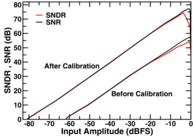
externally. The differential full-scale input range is . The DSM has a sampling rate of 1.1 GHz. Its signal bandwidth is 16.67 MHz if the OSR is 33. Fig. 10 is the mea-sured DSM output spectra before and after the calibration. The input signal is a 3-dBFS 2-MHz sine wave. Without the cali-bration, the quantization noise of the first stage dominates the low-frequency band and is shaped by a 40-dB/decade slope for frequencies above 10 MHz. The calibration signal is visible. It has a frequency of 17.19 MHz. The measured SNR is 57 dB. The SNDR is 54 dB. After the calibration, the quan-tization noise is minimized. The noise floor drops, and the noise at high frequency is shaped by a 80 dB/decade slope. The calibration signal is attenuated by 30 dB. The measured SNR and SNDR become 76 and 74 dB, respectively. If the calibra-tion signal is injected instead of , the tones are 34 dB
Fig. 12. Measured dynamic performance of the DSM.
in the DSM output spectra. Fig. 11 shows the passband details of the output spectra. Before the calibration, the fifth and seventh harmonics are the dominant tones. The spurious-free dynamic range (SFDR) is 58 dB. After the calibration, the third harmonic becomes the dominant tone. The SFDR increases to 83 dB.
Fig. 12 shows the measured SNR and SNDR versus the input signal level. The input is a 2-MHz sine wave. Before the calibra-tion, the peak SNR and the peak SNDR are 57.42 and 54.23 dB, respectively, at 0.71-dBFS input level. The DR is 62 dB. After the calibration, the peak SNR is 77.22 dB at 0.93-dBFS input level, and the peak SNDR is 74.32 dB at 3.85-dBFS input level. The DR increases to 81 dB. Note that, before the cali-bration, there is a visible difference between the SNR and the SNDR for the input level higher than 20 dBFS. This is because the quantization noise leaking to the DSM output contains input harmonics. After the calibration, the leakage is reduced, and the difference between SNR and SNDR is also decreased.
In our design, the opamps employ the constant-current bi-asing scheme. Simulations show that the dc gain of the opamps varies from 10.74 to 8.76 if the temperature changes from 0 C to 80 C. Thus, after calibration, the SNR of the DSM will de-grade by 3 dB if the temperature changes by 10 C. However, this degradation will not occur if the time for the temperature change is much longer than the calibration time constant. On the other hand, the dc gain of the opamp varies from 9.77 to 10.87 if the supply voltage changes from 0.9 to 1.1 V. Thus, after calibration, the SNR degradation is less than 3 dB if the supply voltage variation is less than 50 mV.
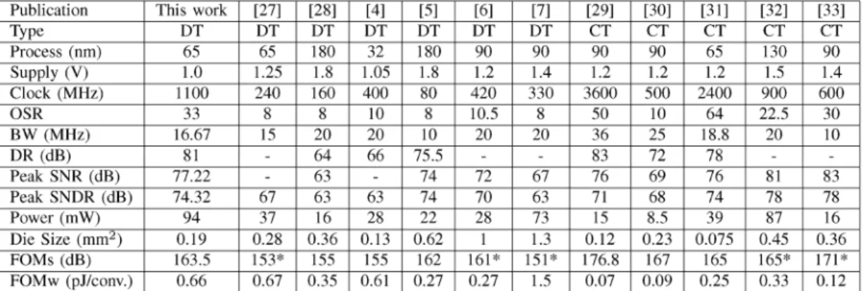
Table III summarizes the performance of this DSM chip and compares it with other wide-bandwidth DSMs. The figure of merit (FOM) are defined as follows [26]:
(14) The FOMs of this chip is 163.487 dB, and the FOMw is 660 fJ/level. Comparing with other discrete-time (DT) DSMs, this DSM has the highest sampling rate, operates under the lowest supply voltage, and achieves competitive FOMs and FOMw. In Table III, the continuous-time (CT) DSMs show better FOMw
2178 IEEE JOURNAL OF SOLID-STATE CIRCUITS, VOL. 48, NO. 9, SEPTEMBER 2013
TABLE III
COMPARISON OFWIDE-BANDWIDTHDSMS
Assume DR equals to peak SNDR or peak SNR. performance. However, they require clocks of more stringent
jitter performance.
VII. CONCLUSION
A fourth-order discrete-time DSM was fabricated using a 65-nm CMOS technology. It has a sampling rate of 1.1 GHz and an input bandwidth of 16.67 MHz with an OSR of 33. We use low-complexity circuits to achieve high speed. The opamps have a unity-frequency of 6 GHz in the integrator configuration, but have a dc gain of only 10. The low-gain opamps result in lossy integrators. We apply the integrator leakage calibration to adjust the leakage-compensating capacitors of the integrators to move their poles back to 1. We use the noise leakage calibra-tion to minimize the quantizacalibra-tion noise of the first loop leaking to the DSM’s combined output. The noise leakage calibration relaxes the matching requirement for the MASH structure. The calibration is simplified since it does not need to correct the coefficients. Both digital calibrations can operate in the background without interrupting the normal DSM operation. The calibration processors are simple digital circuits. They do not have complex filters. The chip’s measured SNDR and DR are 74.32 and 81 dB, respectively. The chip consumes 94 mW from a 1-V supply. The active area is 0.33 0.58 mm .
We demonstrate that the combination of low-complexity cir-cuits and digital calibration can yield a high-speed high-perfor-mance DSM. The design technique is specially suitable for ad-vanced nanoscale CMOS technologies.
APPENDIXA
AVERAGEDTRANSIENTBEHAVIOR OF
As shown in Fig. 1, receives the output . ’s input thresholds are at , and its
corre-sponding digital outputs are . has a
conversion gain of . From Fig. 4, the averaged
variation of for one clock cycle is .
The voltage is expressed as (6). As illustrated in Fig. 5, takes an average of cycles to accumulate from 0 to (or ). Once reaches the threshold, is
changed by 1 and is changed by . Thus, the averaged variation rate is
(15) The above equation leads to (7) and (8).
APPENDIXB
AVERAGEDSTANDARDDEVIATION OF
When the calibration process converges, the behavior of becomes a discrete random fluctuation around 1. If
, alternates between only two values, which are
and , where depending
on . Define the probability for as , and the probability for as . Since the expected value of is
1, i.e., , we have and . If
is given, define the standard deviation of as
(16) If is uniformly distributed from 0 to 1, the standard deviation
of is
(17) The above equation is the same as (9).
ACKNOWLEDGMENT
The authors would like to thank Taiwan Semiconductor Man-ufacturing Company (TSMC), Hsin-Chu, Taiwan, for chip fab-rication under the TSMC University Shuttle Program.
REFERENCES
[1] X. Peng, W. Sansen, L. Hou, J. Wang, and W. Wu, “Impedance adapting compensation for low-power multistage amplifiers,” IEEE J.
Solid-State Circuits, vol. 46, no. 2, pp. 445–451, Feb. 2011.
[2] H. Yoshizawa, T. Yabe, and G. C. Temes, “High-precision switched-capacitor integrator using low-gain opamp,” Electron. Lett., vol. 47, no. 5, p. 315, 2011.
[3] T. Musah and U.-K. Moon, “Correlated level shifting integrator with reduced sensitivity to amplifier gain,” Electron. Lett., vol. 47, no. 2, p. 91, 2011.
[4] B. Carlton, H. Lakdawala, E. Alpman, J. Rizk, Y. Li, B. Perez-Esparza, V. Rivera, C. Nieva, E. Gordon, P. Hackney, C.-H. Jan, I. Young, and K. Soumyanath, “A 32 nm, 1.05 V, BIST enabled, 10–40 MHz, 11-9 Bit, 0.13 mm digitized integrator MASH ADC,” in Proc. Symp.
VLSI Circuits, 2011, pp. 36–37.
[5] S. Lee, J. Chae, M. Aniya, S. Takeuchi, K. Hamashita, P. K. Hanumolu, and G. C. Temes, “A double-sampled low-distortion cascade mod-ulator with an adder/integrator for WLAN application,” in Proc. IEEE
Custom Integr. Circuits Conf., Sep. 2011, pp. 1–4.
[6] P. Malla, H. Lakdawala, K. Kornegay, and K. Soumyanath, “A 28 mW spectrum-sensing reconfigurable 20 MHz 72 dB-SNR 70 dB-SNDR DT ADC for 802.11n/WiMAX receivers,” in IEEE Int. Solid-State
Circuits Conf. Dig. Tech. Papers, Feb. 2008, pp. 496–631.
[7] J. Paramesh, R. Bishop, K. Soumyanath, and D. Allstot, “An 11-Bit 330 MHz 8X OSR modulator for next-generation wlan,” in
Proc. Symp. VLSI Circuits, Dec. 2006, pp. 166–167.
[8] R. Schreier and G. C. Temes, Understanding Delta-Sigma Data
Con-verters. Piscataway, NJ, USA: IEEE, 2005.
[9] J. Silva, X. Wang, P. Kiss, U. Moon, and G. C. Temes, “Digital tech-niques for improved data conversion,” in Proc. IEEE Custom
In-tegr. Circuits Conf., 2002, pp. 183–190.
[10] Z. Zhang, J. Steensgaard, G. C. Temes, and J.-Y. Wu, “A 14-bit dual-path 2-0 MASH ADC with dual digital error correction,” Analog
In-tegr. Circuits Signal Process., vol. 59, no. 2, pp. 143–150, Dec. 2008.
[11] N. Maghari, S. Kwon, and U.-K. Moon, “74 dB SNDR multi-loop sturdy-mash delta-sigma modulator using 35 dB open-loop opamp gain,” IEEE J. Solid-State Circuits, vol. 44, no. 8, pp. 2212–2221, Aug. 2009.
[12] R. Baird and T. Fiez, “Linearity enhancement of multibit A/D and D/A converters using data weighted averaging,” IEEE Trans. Circuits
Syst. II, Analog Dig. Signal Process., vol. 42, no. 12, pp. 753–762, Dec.
1995.
[13] J. Silva, U. Moon, J. Steensgaard, and G. Temes, “Wideband low-dis-tortion delta-sigma ADC topology,” Electron. Lett., vol. 37, no. 12, p. 737, 2001.
[14] J. Silva and G. C. Temes, “Low-distortion delta-sigma topologies for MASH architectures,” in Proc. IEEE Int. Symp. Circuits Syst., 2004, pp. I-1144–I-1147.
[15] R. Schreier, “On the use of chaos to reduce idle-channel tones in delta-sigma modulators,” IEEE Trans. Circuits Syst. I, Fundam.
Theory Appl., vol. 41, no. 8, pp. 539–547, Aug. 1994.
[16] C.-C. Huang and J.-T. Wu, “A background comparator calibration tech-nique for flash analog-to-digital converters,” IEEE Trans. Circuits Syst.
I, Reg. Papers, vol. 52, no. 9, pp. 1732–1740, Sep. 2005.
[17] C.-Y. Wang and J.-T. Wu, “A multiphase timing-skew calibration tech-nique using zero-crossing detection,” IEEE Trans. Circuits Syst. I, Reg.
Papers, vol. 56, no. 6, pp. 1102–1114, Jun. 2009.
[18] C.-C. Huang, C.-Y. Wang, and J.-T. Wu, “A CMOS 6-Bit 16-GS/s time-interleaved ADC using digital background calibration tech-niques,” IEEE J. Solid-State Circuits, vol. 46, no. 4, pp. 848–858, Apr. 2011.
[19] S. Rabii and B. Wooley, “A 1.8-V digital-audio sigma-delta modulator in 0.8- CMOS,” IEEE J. Solid-State Circuits, vol. 32, no. 6, pp. 783–796, Jun. 1997.
[20] K. Nam, S.-M. Lee, D. Su, and B. Wooley, “A low-voltage low-power sigma-delta modulator for broadband analog-to-digital conversion,”
IEEE J. Solid-State Circuits, vol. 40, no. 9, pp. 1855–1864, Sep. 2005.
[21] H. Park, K. Nam, D. Su, K. Vleugels, and B. Wooley, “A 0.7-V 870-W digital-audio CMOS sigma-delta modulator,” IEEE J. Solid-State
Circuits, vol. 44, no. 4, pp. 1078–1088, Apr. 2009.
[22] S.-J. Huang and Y.-Y. Lin, “A 1.2 V 2 MHz BW 0.084 mm CT ADC with 97.7 dBc THD and 80 dB DR using low-latency DEM,” in IEEE Int. Solid-State Circuits Conf. Dig. Tech. Papers, Feb. 2009, pp. 172–173, 173a.
[23] M. Bolatkale, L. J. Breems, R. Rutten, and K. A. A. Makinwa, “A 4 GHz continuous-time ADC with 70 dB DR and 74 dBFS THD in 125 MHz BW,” IEEE J. Solid-State Circuits, vol. 46, no. 12, pp. 2857–2868, Dec. 2011.
[24] D. Schinkel, E. Mensink, E. Klumperink, E. van Tuijl, and B. Nauta, “A double-tail latch-type voltage sense amplifier with 18 ps setup+hold time,” in IEEE Int. Solid-State Circuits Conf. Dig. Tech. Papers, Feb. 2007, pp. 252–253.
[25] B. Nikolic, V. Oklobdzija, V. Stojanovic, and M. Ming-Tak Leung, “Improved sense-amplifier-based flip-flop: Design and measure-ments,” IEEE J. Solid-State Circuits, vol. 35, no. 6, pp. 876–884, Jun. 2000.
[26] V. Singh, N. Krishnapura, S. Pavan, B. Vigraham, D. Behera, and N. Nigania, “A 16 MHz BW 75 dB DR CT ADC compensated for more than one cycle excess loop delay,” IEEE J. Solid-State Circuits, vol. 47, no. 8, pp. 1884–1895, Aug. 2012.
[27] S.-C. Lee, B. Elies, and Y. Chiu, “An 85 dB SFDR 67 dB SNDR 8OSR 240 MS/s ADC with nonlinear memory error calibration,” in Proc.
Symp. VLSI Circuits, Jun. 2012, vol. 1, pp. 164–165.
[28] J. Chae, S. Lee, M. Aniya, S. Takeuchi, K. Hamashita, P. K. Hanu-molu, and G. C. Temes, “A 63 dB 16 mW 20 MHz BW double-sampled analog-to-digital converter with an embedded-adder quantizer,” in
Proc. IEEE Custom Integr. Circuits Conf., Sep. 2010, vol. 1, pp. 1–4,
no. c.
[29] P. Shettigar and S. Pavan, “Design techniques for wideband single-bit continuous-time modulators with FIR feedback DACs,” IEEE J.
Solid-State Circuits, vol. 47, no. 12, pp. 2865–2879, Dec. 2012.
[30] P. Witte, J. G. Kauffman, J. Becker, Y. Manoli, and M. Ortmanns, “A 72 dB-DR CT modulator using digitally estimated auxiliary DAC linearization achieving 88 fJ/conv in a 25 MHz BW,” in IEEE
Int. Solid-State Circuits Conf. Dig. Tech. Papers, Feb. 2012, vol. 24,
no. 3, pp. 154–156.
[31] G. Taylor and I. Galton, “A reconfigurable mostly-digital ADC with a worst-case FOM of 160 dB,” in Proc. Symp. VLSI Circuits, Jun. 2012, pp. 166–167.
[32] M. Park and M. H. Perrott, “A 78 dB SNDR 87 mW 20 MHz bandwidth continuous-time ADC with VCO-based integrator and quantizer implemented in 0.13 m CMOS,” IEEE J. Solid-State Circuits, vol. 44, no. 12, pp. 3344–3358, Dec. 2009.
[33] K. Reddy, S. Rao, R. Inti, B. Young, A. Elshazly, M. Talegaonkar, and P. K. Hanumolu, “A 16-mW 78-dB SNDR 10-MHz BW CT ADC using residue-cancelling VCO-based quantizer,” IEEE J. Solid-State
Circuits, vol. 47, no. 12, pp. 2916–2927, Dec. 2012.
Su-Hao Wu (S’10) was born in Tainan, Taiwan. He
received the B.S. degree in electrical engineering from National Tsing-Hua University, Hsin-Chu, Taiwan, in 2002, and the M.S. degree in commu-nication engineering from National Chiao-Tung University, Hsin-Chu, Taiwan, in 2004, where he is currently working toward the Ph.D. degree in electronics engineering.
His current research interests include high-resolu-tion data converters and low-power mixed-signal in-tegrated circuits.
Jieh-Tsorng Wu (S’83–M’87–SM’06) was born in
Taipei, Taiwan. He received the B.S. degree in elec-tronics engineering from National Chiao-Tung Uni-versity, Hsin-Chu, Taiwan, in 1980, and the M.S. and Ph.D. degrees in electrical engineering from Stanford University, Stanford, CA, USA, in 1983 and 1988, re-spectively.
From 1980 to 1982, he served in the Chinese Army as a Radar Technical Officer. From 1982 to 1988, at Stanford University, he focused his research on high-speed analog-to-digital conversion in CMOS VLSI. From 1988 to 1992, he was a Member of Technical Staff with Hewlett-Packard Microwave Semiconductor Division, San Jose, CA, USA, where he was respon-sible for several linear and digital gigahertz IC designs. Since 1992, he has been with the Department of Electronics Engineering, National Chiao-Tung Univer-sity, Hsin-Chu, Taiwan, where he is now a Professor. His current research inter-ests are high-performance mixed-signal integrated circuits.
Dr. Wu is a member of Phi Tau Phi. He has served as an associate editor of the IEEE JOURNAL OFSOLID-STATECIRCUITS. Since 2012, he has served on the Technical Program Committee of the International Solid-State Circuits Conference (ISSCC).