IEEE ELECTRON DEVICE LETTERS, VOL. 17, NO. 5 , MAY 1996 229
5
mm High-Power-Density Dual-Delta-Doped
Power HEMT's for
3 V L-Band Applications
Yeong-Lin
Lai,
Edward Y. Chang,Member, IEEE,
Chun-Yen Chang,Fellow,
IEEE,
T. K.
Chen,T. H. Liu,
S. P.
Wang,T.
H.
Chen,and
C. T. Lee
Abstract- A high-power-density dual-&doped AlGaAs/ InGaAdGaAs high electron mobility transistor (HEMT) for personal communication applications has been developed. A 5.0 mm gate-width device operating at a drain bias of 3.0 V
gave an output power over 1 W. The 1 pm gate-length HEMT exhibited a current density of 425 mA/mm at T i s = 0.5 V. The maximum transconductance of the device was 270 mS/mm. The effective knee voltage was as low as 0.3 V. At the class AB operation, the HEMT demonstrated an output power density of 200 mW/mm, 64% power-added efficiency and 18.2 dB linear gain at 900 MHz. This is the highest power density of a dual-b-doped AlGaAs/lnGaAs/GaAs HEMT reported to date for low voltage (3 V) wireless applications.
I. INTRODUCTION
DVANCED high-performance wireless communication
A
systems require high-efficiency power transistors oper- ating at low supply voltage. The advantages of low operation voltage include: (1) reduction of power consumption of the circuits, (2) decreasing the number of the battery cells, and(3) reduction of the size and weight of the systems. Recently, high-efficiency GaAs MESFET's used for cellular telephone applications were reported [ 11, [2]. However, the operation voltage of these devices is still high (4.7 V). As the operation voltage is lowered, the output power of the devices will drop drastically. In order to increase the output power of the devices operating at 3 V, large peripheries with gate width of 14-16 mm were used [ 3 ] , [4]. The large gate width of the devices have the following problems: The large gate width increases the chip size and causes a low chip yield which are undesired and unaccepted from the production standpoint of
view. Furthermore, increasing in the gate width decreases the output impedance and leads to difficult output matching. The large gate width is also associated with an increase of the total gate leakage current and makes the quiescent gate bias point unstable [5]. In this work, we develop a 5.0 mm gate-width Manuscript received November 14, 1995; revised January 9, 1996. This work was supported in part by the National Science Council, Republic of
China, under Contract NSC-84-2215-E009-024.
Y.-L. Lai is with the Department of Electronics Engineering and Institute of Electronics, National Chiao Tung University, Hsinchu 300, Taiwan, ROC. E. Y. Chang and T. K. Chen are with the Institute of Materials Science and Engineering, National Chiao Tung University, Hsinchu 300, Taiwan, ROC.
C.-Y. Chang is with the Department of Electronics Engineering and Institute of Electronics, National Chiao Tung University, and National Nano Device T. H. Liu, S. P. Wang, and T. H. Chen are with Hexawave Photonic Systems, C. T. Lee is with the Institute of Optical Sciences, National Cental Publisher Item Identifier S 0741-3 106(96)03737-8.
Laboratories, Hsinchu 300, Taiwan, ROC. Inc., Hsinchu 300, Taiwan, ROC. University, Chungli 320, Taiwan, ROC.
high-power-density dual-&doped AlGaAs/InGaAs/GaAs high electron mobility transistor (HEMT) for 3.0 V L-band wireless communication applications. The device when operated at 3.0 V supplied over 1 W output power at 900 MHz. The high output power was achieved by small gate periphery at low operation voltage. The developed HEMT eliminates the problems of large periphery while having the advantages of low operation voltage.
11. DEVICE FABRICATION
The structure of the dual-6-doped AlGaAs/InGaAs/GaAs HEMT, as shown in Table I, was grown by molecular-beam- epitaxy (MBE) on a (100) semi-insulating GaAs substrate. The structure consists of a 0.6-pm-thick undoped GaAs buffer layer, a 20-periods undoped AlGaAdGaAs superlattice buffer, then an undoped GaAs buffer again. The active part of the structure is an 85
A
In0 ZlGao 79As channel layer sandwiched between an upper 35 8, undoped A10 21Gao 79As layer and alower 40
A
undoped GaAs layer. The two dimensional elec- tron gas (2-DEG) was formed in the pseudomorphic InGaAs channel by electron transfer from silicon S-doping above and below the InGaAs layer. The dual-6-doped structure provides high carrier concentration in the InGaAs channel and leads to high current density and high transconductance ( g m ) whichbenefits the power performance of the device. An undoped Alo zlGao 7 9 A ~ Schottky barrier layer was grown on the upper S-doping layer to obtain high gate-to-drain breakdown voltage (BV&). Both high current density and high breakdown voltage are important for a power device. Finally, a heavily Si-doped
( 5 x 10'' cmp3) GaAs cap layer was formed to provide the good ohmic contact and reduce the source resistance. The fabricated device had a total gate width of 5.0 mm with 1 .O pm gate length for each finger, as shown in Fig. 1. The device isolation was accomplished by wet etching with HF:H202:H20 etchant. The ohmic metal, Au/Ge/Ni, was deposited by electron-beam evaposition followed by rapid thermal annealing at 300°C for 10 s. The 1.0-pm-long Ti/Pt/Au gate was defined by the standard photolithography. Silicon nitride (Si3N4) was used for device passivation.
111. DEVICE PERFORMANCE
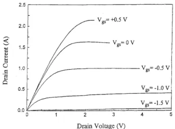
Fig. 2 shows the current-voltage (I-V) characteristics of the 5 mm-wide dual-&doped power HEMT's. The maximum drain current density (I,,,), defined as the drain saturation current density measured at a gate-to-source voltage (Vg5) of +0.5 V, is 425 mA/mm. The maximum transconductance ( g T n ) is 0741-3106/96$05.00 0 1996 IEEE
230 IEEE ELECTRON DEVICE LETTERS, VOL. 17, NO. 5 , MAY 1996 - - Gate width = 5 mm Drain bias = 3 V Fig. 1.
HEMT with 5-mm gate width and I-pm gate length.
Photograph of fabricated dual-6-doped AlGaAsflnGaAsiGaAs power
30 h E rn
u,
(r 2 5 -$
f?
+
20 3a
TABLE I DEVICE STRUCTURE OF HEMTPROFILE THICKNESS
N+GaAs 400A
undoped AlGaAs 350A
Si delta-doping
undoped AlGaAs 35A
undoped InGaAs 85A
undoped GaAs 40A
-
-
Si delta-doping undoped AlGaAs k 15 200A -undoped GaAs j0o.A
undoped AlGaAsiGaAs supperlattice undoped GaAs
semi-insulating GaAs substrate
270 mS/mm. These values are higher than those of MESFET's (I,,, = 312 mA/mm, gm = 106 mS/mm) [3] and HFET's (Imax = 220 mA/mm, gnL = 200 mS/mrn) [SI. Both the higher drain current density and transconductance are attributed to the dual-&doped HEMT structure. The pinch-off voltage (V,) of the HEMT's is about -1.7 V. The effective knee voltage. defined as the drain bias (V&) value when the drain current
(Id,) becomes 100 mA/mm with V,, = $0.5 V, is 0.3 V which is comparable to and even lower than the reported values [3]-[SI. The on resistance, defined as Vds/Ids with V,, = 0
V.
is about 3.3 ohms-mm. The gate-to-drain breakdown voltage. defined at a gate current of 1 mA/mm, is more than 14 V. This value is competitive to those of HFET's and MESFET's (BV,d = 10 V) [41, [61, VI.The S-parameter measurements of the devices were per- formed from 0.5 to 10 GHz for the 1 mm-wide devices using
an automatic network analyzer. Based on the 5'-parameter data, the unity short-circuit current-gain frequency
(
f t ) and the maximum frequency of oscillation (.fmaX) can be computed. The f t and fmax estimated at V,, = -0.6 V and V,, = 3.0 V are 19 GHz and 58 GHz, respectively.Power performance of the HEMT's was measured at 900 MHz with a drain bias of 3.0 V. The device was operated under the class AB condition with a bias drain current of 0.3 A. The power characteristics were measured by a power tuning system, in which the input and output tuners with variable capacitors and inductors were used to provide the conjugate matched input and load impedances for the optimum power performance. The 5 mm-wide device exhibits an output power over 1 W, corresponding to a power density over 200 mW/mm. This is the highest power density ever achieved with power devices at such a low operation voltage. The power-added efficiency of 64% and the linear gain of 18.2 dB were obtained
h
4
V, = +0.5 V 2.0 -v,
=
0v
1.5 2.0 - V,,= -0.5 Vv,,=
-1.0v
V,,= -1.5 V 1.01
v,,=
-1.0v
V,,= -1.5 V 0 1 2 3 4 5 Drain Voltage (V) Fig. 2. power HEMT.Typical current-voltage characteristics of 5 mm-wide dual-6-doped
n
a
10 " '
/-,
" ' ' ~ * ' ~ * " ~ ' ~ ' ~ ~0 ' ( ' "-10 -5 0 5 10 15 20 25
INPUT POWER (dBm)
Fig. 3. Output power and power-added efficiency as a function of input power for 5 mm-wide dual-&doped AlGaAshGaAsiGaAs power HEMT at 900 MHz and drain bias of 3.0 V.
at 900 MHz. The output power and power-added efficiency as a function of the input power are depicted in Fig. 3. The most significant results in this work is that the high performance of the output power, the power-added efficiency, and the linear gain is achieved by the small gate periphery. This feature leads to high yield, low cost, and easy impedance matching.
The load-pull measurement of the 5 mm HEMT at 900
MHz was accomplished by the power tuning system and the automatic network analyzer. The load impedance associated with the optimum power performance at a drain bias of 3.0 V is Z L = 7.82 - j 2 . 4 ohms (I'L = 0.731 1-173.62'). This load-pull data can be used to build up a power module for low voltage wireless communication applications.
LA1 et al.: DUAL-DELTA-DOPED POWER HEMT’S 23 1
The developed high-power-density dual-6-doped Al- GaAs/InGaAs/GaAs HEMT demonstrated good potential for the applications of analog cellular phone systems, such as AMPS (Advanced Mobile Phone Service), ETACS (Enhanced Total Access Communication System), etc. The HEMT can be applied to the output stage o f the analog cellular phone power module, in which the device operates at the class AB condition to supply high output power in the active mode and maintain low power consumption in the standby mode.
IV. CONCLUSION
A high-power-density dual-6-doped AlGaAs/InGaAs/GaAs HEMT has been developed. A 5.0 mm gate-width device operating at a drain bias of 3.0 V supplies over 1 W output power at 900 MHz. The I bm gate-length HEMT exhibited a current density of 425 mA/mm (at V,,S = 0.5 V), a maximum transconductance of 270 mS/mm. The effective knee voltage was as low as 0.3 V. At 900 MHz, the HEMT demonstrated an output power density of 200 mW/mm, a power-added effi- ciency of 64% and linear gain o f 18.2 dB. These outstanding performance was due to the high current density and high electron mobility of the dual-6-doped HEMT device. This is the highest power density reported for 3 V L-band wireless applications. The high output power achieved by small gate periphery leads to high yield, low cost, and easy impedance
matching. The optimized dual-6-doped AlGaAsfinGaAdGaAs structure demonstrates excellent power performance and is a potential candidate for low voltage wireless communication applications.
REFERENCES
[ 11 Y. Ota, M. Yanagihara, C. Axuma, M. Maeda, and 0. Ishikawa, “Highly efficient, very compact GaAs power module for cellular telephone,” in ZEEE MTZ-S ~ i ~ . , - p p . isi7-is20, 1992.
121 0. Ishikawa. Y. Ota, M. Maeda. A. Tezuka. H. Sakai. T. Katoh, J. Itoh.
. _
Y. Mori, M. Sagawa, and M. Inada, “Advanced technologies of low- power GaAs IC’s and power modules for cellular telephones,” in GuAs
IC Symp. Tech. Dig., pp. 131-134, 1992.
131 J. L. Lee, H. Kim, J. K. Mun, H. G. Lee, and J. M. Park, “2.9 V operation GaAs power MESET with 31.5-dBm output power and 64% power-added efficiency,” IEEE Electron Device Lett., vol. 15, no. 9, pp. 324-326, Sept. 1994.
[4] K. Inosako, K. Matsunaga, Y. Okamoto, and M. Kuzunara, “Highly efficient double-doped heterojunction FET’s for battery-operated portable power applications,” IEEE Electron Device Lett., vol. 15, no. 7, pp. 248.250, July 1994.
[SI N. Iwata, K. Inosako, and M. Kuzunara, “3 V operation L-band power double-doped heterojunction FET’s,” in IEEE MTT-S Dig., pp. 1465-1468, 1993.
[6] S. Mural, T. Sawai, T. Yamaguchi, S . Matsushita, and Y. Harada, “A high power-added efficiency GaAs power MESFET operating at a very low drain bias for use in L-band medium power amplifiers,” in GaAs
IC Symp. Tech. Dig., pp. 139-142, 1992.
171 P. O’Sullivan, G. St. Onge, E. Heaney, F. McCrath, and C. Kermarrec, “High performance integrated PA, T/R switch for 1.9 GHz personal communications handsets,” in GuAs IC Symp. Tech. Dig., pp. 33-35,