國 立 交 通 大 學
電子工程學系 電子研究所碩士班
碩士論文
a-IGZO 薄膜電晶體的製作與特性分析
Fabrication and Characterization of
a-IGZO Thin Film Transistors
研 究 生: 張維軒
指導教授: 林鴻志 博士
黃調元 博士
a-IGZO 薄膜電晶體的製作與特性分析
Fabrication and Characterization of a-IGZO Thin
Film Transistors
研究生: 張維軒 Student: Wei-Hsuan Chang
指導教授:林鴻志 博士 Advisors:Dr. Horng-Chih Lin
黃調元 博士 Dr. Tiao-Yuan Huang
國立交通大學
電子工程學系 電子工程研究所
碩士班論文
A Thesis
Submitted to Department of Electronics Engineering & Institute of Electronics College of Electrical and Computer Engineering
National Chiao-Tung University In Partial Fulfillment of the Requirement
For the Degree of Master of Science
In
Electronics Engineering
July 2013, Hsinchu, Taiwan, Republic of China
i
a-IGZO 薄膜電晶體的製作與特性分析
研 究 生 : 張 維 軒 指 導 教 授 : 林 鴻 志 博 士
黃調元 博士
國立交通大學
電子工程學系 電子研究所碩士班
摘要
由於 a-IGZO 具有在非晶下較高的載子遷移率,加上利用射頻濺鍍的低溫製程和大 面積的均勻性,使得 a-IGZO 非常適合作為將來面板的主要材料。在本篇論文當中,我 們成功的利用了射頻濺鍍的方式製造 a-IGZO 薄膜電晶體。藉由調整製程過程中的氧流 量與沉積的時間,我們研究不同沉積氧流量下以及不同通道厚度下 a-IGZO 電晶體的特 性。為了提升電性,我們也製造了兩層通道的結構。 有鑑於我們所製作的元件中出現奇怪的 hump 現象,因此我們也使用了變頻量測的 方式去萃取 density of state (DOS) 來解釋。並且為了改善 hump 現象,我們使用了真 空退火的方式,去改善其電性。針對可靠度方面,我們也討論環境的氣體分子對於元件電性的影響,同樣地使用退 火的方式來改善。由於使用於面板的元件會經常處於照光和偏壓的條件之下,所以諸如 positive bias stress,negative bias stress,light stress,positive bias light stress 和 negative bias light stress 等特性也作了測試與討論。
ii
Fabrication and Characterization of a-IGZO
Thin Film Transistors
Student: Wei-Hsuan Chang Advisors: Dr. Horng-Chih Lin
Dr. Tiao-Yuan Huang
Department of Electronics Engineering & Institute of Electronics National Chiao-Tung University, Hsinchu, Taiwan
Abstract
With the high mobility of IGZO material in the amorphous phase, and the merits of low process temperature and large area uniformity associated with the RF sputter, a-IGZO is widely considered as one of the most promising materials for the manufacturing of flat-panel displays. In this thesis, we have successfully fabricated a-IGZO TFTs by RF sputter. We studied the effects of different deposition oxygen flow and the channel thickness on the device performance. In addition, we have also fabricated a-IGZO TFTs with double active layers for improving the electrical performance.
In order to explain the strange hump phenomenon in our studies, multi-frequency CV measurements were used to extract the DOS. We also found that a vacuum annealing is useful for eliminating the hump phenomenon.
For reliability issues, we have studied the effects of the surrounding ambient gas molecules, and used vacuum annealing for improvements. The instability of positive bias stress, negative bias stress, light stress, positive bias light stress and negative bias light stress were also investigated.
iii
Acknowledgement
碩士班這兩年過的比想像中的還要快,而碩士的結束也代表著求學生涯的正式落幕。 兩年裡學到許多,很慶幸當初自己可以來到交大,來到 ADTL 這個 Lab, 還記得第一年的 meeting 幾乎每次都會犯錯被老師念,到後來被念的次數漸漸的減少, 這應該表示著自己或多或少有點成長吧。實驗的過程中也遇到許多挫折,還記得有陣子 我的 devices 怎麼作怎麼死,但也都一一克服了。 很感謝這兩年裡,林鴻志老師和黃調元老師的指導,大概我們從碩一開始的不成熟 真的常讓老師們的血壓飆高。也很謝謝博班學長們在我們遇到問題時候的幫忙,特別感 謝阿哲哥好幾次早上六七點起來 train 我機台還有幫我 coating。還有同屆的大家,王 佳文,李信宏,吳明鴻,洪湘婷,鄭靜玲,大家在這兩年裡總是互相幫忙,實驗上,功 課上都是,儘管畢業的此刻,有些人選擇留下念博班,而非一起離開學校,步入社會。 然而,儘管選擇不同的人生旅途,但這兩年的相處多少都會在彼此的人生裡留下一點痕 跡,回憶中會有第一個勇敢簽博的明鴻,還有一百公尺外就可以聽到她笑聲的靜玲,未 來繼續和我當同事的信宏,後來當我鄰居的湘婷,還有常常被女友拒接電話的佳文,都 會是將來回憶裡的一環。 兩年中從各方面挫折漸漸的成熟,這段時間家人的支持真的讓人心懷感激,縱使家 裡有了些變化,但果然還是家人的陪伴才是面對挫折最好的良藥。還有雙胞胎弟弟張維 祐在一些軟體的使用上真的幫了我大忙。最後大概就是因為王佳文的牽線認識的妳,雖 然時間不長卻也是我碩班生涯裡很重要的回憶和支持。 兩年裡總想著快點畢業,想快點離開學生生涯,充滿著對成長的憧憬,但真的到了 這個時候還是充滿著許多的不捨,和對於未來不安與期待。希望碩士班這個對我而言人 生重要的分水嶺可以一直像此刻一般,每當回想起時總有各式各樣的感動。 張維軒 誌於 風城交大 2013 年 7 月iv
Contents
Abstract (Chinese)………. i
Abstract (English)………. ii
Achnowledge (Chinese)………... iii
Co nent s………. iv
List of Figure Captions………. vi
Chapter 1 Introduction………...……1
1.1 General Background od Metal-Oxide-Semiconductor Thin-Film Transistors…...1
1.2 Overview of a-IGZO TFTs……….5
1.3 Motivation and Objective of this Thesis……….8
1.4 Organization………....8
Chapter 2 Device Fabrication and Measurement Setup……… 10
2.1 Device Fabricat io n and Process Flow………10
2.2 Measurement Setup……….………12
Chapter 3 Results and Discussion………15
3.1 Effects of Deposition Oxygen Flow………15
3.2 Effects of Active Layer Thickness………17
3.3 Effects of Surrounding Ambient………..19
3.4 Impact of Different Gate Dielectric Thickness and Channel Materials………20
v
3.6 Effects of Vacuum Annealing……….…....……..22
3.7 Effects of Bias Stress and Light Stress……….…23
Chapter 4 Conclusion………. 27
4.1 Conclusio n.………. 27
References………29
Figure Capt io ns………..37
vi
List of Figure Captions
Chapter 1
Tab.1.1. Comparison of a-Si, Poly-Si and amorphous oxide TFTs………..37 Fig.1.1. Schematic drawings for the carrier transport paths (that is, conduction band bottoms) in the crystalline and amorphous semiconductor. (a) covalent semiconductor, for e x a m p l e , s i l i c o n . ( b ) p o s t t r a n s i t i o n m e t a l o x i d e semiconductors……….………….38 Fig. 1.2. (a) The potential barrier formed by random distribution of Ga3+ and Zn2+ ions, and with a low Fermi level which can’t induced enough electron for conduction (b) electrons trickle through potential valley as Ef increase (c) the Fermi level is high enough to immerse whole potential barriers so that electrons almost unhindered (d) p e r c o l a t i o n c o n d u c t i o n m o d e l ( i ) a s h o r t e r p a t h ( i i ) a l o n g e r path……….….40 Fig. 1.3. Schematic models of subgap DOS in (a) a-Si:H (b) a-IGZO TFTs………...…41 Fig. 1.4. Comparison of the DOS between a-Si:H and a-IGZO films………….……….42
Chapter 2
Tab.2.1. Major deposition parameters for preparing the a-IGZO films………....……43 Tab.2.2. Major deposition parameters for preparing S/D electrodes……….……...44 Fig.2.1. (a) The deposition rate as a function of power at constant oxygen flow (1 sccm), and (b) as a function of oxygen flow at fixed power (100 W)……….45 Fig.2.2. (a) The deposition rate as a function of power at constant oxygen flow (1sccm), and (b) as a function of oxygen flow at fixed power (100 W) (c) An a-IGZO channel film was deposition by RF sputter (d) Definition of the source/drain regions with PR patterns (e) Formation of source/drain metal deposition with lift-off method (f)
vii
Coating of a PR layer (g) Exposure and (h) patterning of the active region by wet etching (i) Cross-sectional view of the a-IGZO TFTs device with single active layer (j) with double active layer……….…47 Fig.2.3. (a) Two-element capacitance model. (b) Four-element capacitance model. (c) Physics-based capacitance model. (d) Equivalent model for frequency independent Cg composed of Cox, CLO C, CFREE (e) Physics-based model of CLO C and
CFREE………..48
Fig.2.4. Measured C-V characteristics with various measurement frequencies, and the conductance characteristics (inset)……….……….49 Fig.2.5. Impedance versus frequency (inset) and the series resistance, Rs versus the
gate-to-source voltage……….……49 Fig 2.6. Gp
ω obtained by Eq. 2.12 and the circle represents the maximum value of ω at
ωτ = 1……….………..50
Chapter 3
Fig. 3.1 Transfer characteristics of a-IGZO devices with oxygen flow of (a) 0 sccm, (b) 1 sccm, (c) 3 sccm, (d) 5 sccm. In each figure several devices are measured in order to check the variation in device performance………..……….52 Fig. 3.2 Typical transfer characteristics of a-IGZO devices deposited with different oxygen flow rates……….53 Fig. 3.3 (a) Extracted mobility, threshold voltage and (b) on/off ratio, subthreshold swing as a function of oxygen flow rate………...54 Fig. 3.4 (a) Extracted voltage-dependent mobility of a-IGZO TFTs as a function of gate voltage. (b) Extracted series resistance as a function of gate voltage for a-IGZO TFTs deposited with different oxygen flow rate………...………55
viii
Fig. 3.5 Comparison of transfer characteristics of a-IGZO devices deposited with different oxygen flow at (a) Vd=0.1, 1 V, and (b) Vd=0.1, 4V………56
Fig. 3.6 Transfer characteristics of a-IGZO devices deposited with different oxygen flow measured by positive and negative voltage sweeps………..……..57 Fig. 3.7 Multi-frequency CV characteristics of a-IGZO TFTs with deposition oxygen flow at (a) 0 sccm and (b) 1 sccm………..…….58 Fig. 3.8 Multi-frequency CV characteristics of a-IGZO TFTs with deposition oxygen flow at (a) 3 sccm and (b) 5 sccm………..…….59 Fig. 3.9 Extracted frequency-independent capacitance of a-IGZO devices deposited with different oxygen flow………..……60 Fig. 3.10 Extracted DOS of a-IGZO devices deposited with different oxygen flow...60 Fig. 3.11 Output characteristics of devices with the channel film deposited at oxygen flow of (a) 0 sccm (b) 1 sccm (c) 3 sccm and (d) 5 sccm………...62 Fig. 3.12 Transfer characteristics of a-IGZO devices with channel thickness of (a) 10 nm, (b) 15 nm, and (c) 20 nm………..………64 Fig. 3.13 Comparison of transfer characteristic of a-IGZO devices with different channel thickness at (a) Vd=0.1 and (b) Vd=0.1 and1 V………..………65
Fig. 3.14 (a) Extracted mobility, threshold voltage and (b) on/off ratio, subthreshold swing as a function of channel thickness……….………...66 Fig. 3.15 (a) Extracted mobility and (b) extracted series resistance as a function of gate
v o l t a g e f o r a - I G Z O T F T s d e p o s i t e d w i t h d i f f e r e n t c h a n n e l thickness……….……….67 Fig. 3.16 Multi-frequency CV characteristics of a-IGZO TFTs with channel thickness of (a)10 nm, (b)15 nm, and (c)20 nm……….69 Fig. 3.17 Extracted frequency-independent capacitance of a-IGZO devices with different
ix
channel thickness………...……….70 Fig. 3.18 Output characteristics of devices with channel thickness of (a) 10 nm, (b) 15 nm, and (c) 20 nm………..72 Fig. 3.19 Transfer characteristics of a-IGZO TFTs measured before and after exposure to an ambient of high humidity………….……….…72 Fig. 3.20 Transfer characteristics of a-IGZO TFTs measured at different partial pressure of (a) air and (b) oxygen……….………..73 Fig. 3.21 A physical model showing the adsorption of (a) O2 and (b) H2O molecular on the
surface of an IGZO film and the interaction between the adsorbed species and the electrons in the film……….………..74 Fig. 3.22 Comparison of transfer characteristics of a-IGZO TFTs with different channel thickness measured as-fabricated and three months later………...74 Fig. 3.23 Comparison of transfer characteristics of a-IGZO TFTs with different deposition o x y g e n f l o w r a t e m e a s u r e d a s - f a b r i c a t e d a n d t h r e e m o n t h s later……….…….75
Fig. 3.24 (a) Transfer characteristics and (b) extracted mobility of a-IGZO TFTs with gate dielectric thickness of 10 nm and 50 nm……….76
Fig. 3.25 Comparison of transfer characteristics of a-IGZO and ITO TFTs………77 Fig. 3.26 Transfer characteristics of a-IGZO TFTs with double active layer with deposition
oxygen flow of 1, 1/3, 3/1, 1/5 and 5/1 sccm at Vd=0.1 V………...78
Fig. 3.27 (a) Comparison of the transfer characteristics of a-IGZO devices deposited with different oxygen flow measured as-fabricated, 3 months later, and (then) after 30 min annealing in vacuum at 300 oC. (b) Comparison of Vth of a-IGZO devices m e a s u r e d a t d i f f e r e n t s t a g e s a s a f u n c t i o n o f t h e o x y g e n low………...79
x
Fig 3.28 (a) Transfer characteristic for positive and negative sweep with deposition oxygen flow fixed at 1, 1/3 and 1/5 sccm, transfer characteristics of a-IGZO devices after vacuum annealing for single active layer and double active layer of 1/3 and 1/5 sccm at (b) Vd=0.1 V and (c) Vd=4 V………...…………81
Fig. 3.29 Transfer characteristics of a-IGZO devices with channel thickness of 10 nm subjected to (a) PBS, (b) NBS, (c) LS, (d) PBLS, and (e) NBLS for 0 ~ 1000 s……….84 Fig. 3.30 Electron trapping mechanism under a positive bias stress …...………84 Fig. 3.31 Comparison of transfer characteristics of a-IGZO devices with channel thickness of
1 0 n m s u b je c t e d t o P B S , N B S , L S , P B L S a n d N B L S fo r 3 0 0 s……….…85 Fig. 3.32 Extracted mobility of a-IGZO TFTs subjected to various stress modes as a function of gate voltage………...85 Fig. 3.33 Transfer characteristics of a-IGZO devices with channel thickness of 20 nm subjected to (a) PBS and (b) NBS………...86 Fig. 3.34 Comparison of transfer characteristics of a-IGZO devices with channel thickness of 2 0 n m s u b je c t e d t o P B S , N B S , L S , P B L S a n d N B L S fo r 3 0 0 s……….………87
1
Chapter 1
Introduction
1.1
General background of Metal-Oxide-Based Thin Film Transistors
Active-matrix liquid crystal displays (AMLCDs) and active-matrix organic light-emitting diodes (AMOLEDs) are nowadays mainstream commodities in our daily life. Typically, hydrogenated amorphous silicon (a-Si:H) thin-film transistors (TFT) are used as the switching transistors in these applications [1-7]. But due to its low mobility (< 1 cm2/Vs), it can’t afford the requirement of the market for the high-performance displays [1-7]. Although the high mobility of low-temperature polycrystalline silicon (LTPS) may be a resolution, non-uniformity in device performance caused by the size variation of grains hinders the manufacturing of this technology in large-area displays [2-3][5]. Thus its application is limited in the small-size commodities such as mobile phones. From the background mentioned above, semiconductors of high carrier mobility and amorphous phase are suitable for flat-panel display applications. If we want to manufacture the display on a flexible substrate, low process temperature should also be considered. Also in recent years the transparent display is another focus [1-6]. To satisfy the demand of high-performance, low process temperature, and even transparency, transparent conducting oxide (TCO) technology are most promising. A comparison of a-Si:H, poly-Si and amorphous oxide TFTs are shown in Table 1.1 [8].
Though using TCO as the channel layer was reported forty years ago [1], almost as early as the first cadmium sulfide (CdS) TFT reported by Weimer [1][9-10], it’s research activities didn’t come into notice until 2000 and beyond, especially in 2003 when Holffman demonstrated ZnO TFTs with a good performance and visible potential for replacing
2
traditional a-Si:H TFTs [1][11].
These researches on TCO TFTs can be divided into three categories which are IGZO, ZnO, and other metal oxide semiconductor including In2O3, SnO2, ZTO, ITO, IZO, IGO and
so on. These materials are often with a wide band gap (>3 eV) that allows it to be transparency and with the mobility (3-50 cm2/Vs) higher than the a-Si:H even in the amorphous phase, making it a candidate to replace a-Si:H and LTPS [1-6].
The reason that TCOs have the higher mobility than a-Si:H could be attributed to the properties of the electronic orbitals of valence electrons, as explained by Nomura at al. in 2004 [12]. The sp3 orbitals of the covalent semiconductors are with high directionality. Although carriers have high mobility in crystalline covalent semiconductors, the amorphous phase would alter the bond angle and significantly change the electronic levels, leading to the generation of tail-states which devastate the mobility. On the other hand, the amorphous oxide semiconductors (AOS) commonly consist of heavy post-transition-metal cations with an electronic configuration of (n-1)d10ns0, (n≧4 and is the principle quantum number) which the spherical s-orbitals can directly overlap with the neighboring ns orbitals (Fig. 1.1 (a) (b)) [12]. Since the overlap is insensitive to the distortion of the chemical bonds, the amorphous phase of the AOS could exhibit a mobility comparable to that in the crystalline phase [1-6][12].
ZnO is one of the most widely studied AOS materials due to its electrical performance good enough to satisfy the application requirements mentioned above. However, it forms polycrystalline phase even when deposited at room temperature and the existence of grain boundaries tends to deteriorate the electrical performance, uniformity, and stability of the fabricated devices. In view of this, Indium-Gallium-Zinc-Oxide (IGZO) was proposed to serve as the active layer of TFTs [1].
IGZO is a multicomponent oxide material, and the different coordinate numbers of these atoms allow IGZO to have amorphous phase. Because of the spherical valence orbital, IGZO
3
still remain mobility over 10 cm2/Vs in the amorphous phase. Also the high on/off ratio (over 106), suitable carrier concentration (<1015 cm-3), low process temperature (near room temperature) and transparency make IGZO a feasible material for mass production. Indium, gallium, zinc and oxide plays different roles in IGZO TFTs. Indium influences the mobility very much, since it is one of the major composition of the conduction band minimum. In content is expected to enhance the mobility and elevate the on current since the incorporation of In will broad spread conduction band minimum. However the accompanied non-controllable channel conductivity as In incorporation is too high would cause low Ion/off
due to the dramatic rise in off current. Gallium content can suppress carrier generation via oxygen vacancy because of the stronger chemical bond of Ga-O than Zn-O and In-O bonds. Thus adding Ga is one of the effective methods to control the carrier concentration and lower the off current. By increasing zinc content, subthreshold swing can be improved because of its ability to modulate the shallow tail states below the conduction band minimum and repair the interfacial states at the gate and channel interface. Moreover, from the point of the material phase, ZnO and In2O3 are crystalline phase even deposited at room temperature. Depending
on the size and ionic charges, the incorporation of two or more cations will enhance the chance to form the amorphous state [1-6] [13].
Carrier transport mechanism is another issue for AOS TFTs, since the mechanism is totally different from traditional a-Si:H TFTs. For traditional silicon-based TFTs, mobility will decrease as the carrier concentration increases due to the impurity scattering [14]. In contrast the mobility increase with increasing carrier concentration for AOS-based TFTs. This could be explained by percolation conduction theory [13] [14]. The random distribution of Ga3+ and Zn2+ will form the potential barriers and the barrier heights are lowered when the carrier concentration increases beyond ~1019 cm-3, thus the mobility are increased as well. [12] This is illustrated in Figs. 1.2 (a)-(c). The electrical conductivity shows thermal dependence
4
when the carrier concentration is less than 1019 cm-3 [14]. Since the electrons will take a shorter and higher conduction path at a higher temperature (Fig. 1.2 (d)), the conductivity increases when temperature increases. The conductivity is temperature independent when the carrier concentration exceeds 1019 cm-3 since the Fermi level is high enough and most of the potential barriers are immersed under the Fermi level so that the electron conduction path is almost unhindered [14].
Characteristics of density-of-states (DOS) in the channel are also different between conventional a-Si:H TFTs and AOS (here using a-IGZO as an example) TFTs. As shown in Fig. 1.3 (a), a-Si:H TFTs have a high amount of tail states below conduction band minimum (CBM) and above valance band maximum (VBM). In the figure donor and acceptor levels are also labeled [8]. For a-IGZO the tail states also exists, but the distribution is asymmetry that the valence band edge has a much higher density, as shown in Fig. 1.3 (b). In the figure we can further separate the subgap DOS (Dsg) into donor level, localized states, and traps for slow
photocurrent [3]. A comparison in DOS between a-IGZO and a-Si:H films is given in Fig. 1.4 [3] in which the Dsg near the CBM of a-IGZO is about one order in magnitude lower than that
5
1.2 Overview of α- IGZO TFTs
There have been many studies about a-IGZO TFTs reported in recent years. Here we just briefly highlight some of the observations which are concerned in this work, including the effects of oxygen flow, channel layer thickness, plasma treatment, passivation, annealing, S/D electrode. Several electrical parameter extraction methods are also discussed.
The oxygen partial pressure during deposition would significantly affect the electrical properties of a-IGZO TFTs [24-26]. The Vth was found to shift positively when the oxygen partial pressure is increasing [24]. The higher oxygen partial pressure is expected to compensate the oxygen vacancies and thus reduce the free carrier concentration [24].
Changing the thickness of the active layer is one of the easiest way to adjust the electrical performance of a-IGZO TFTs [27-31]. As proposed in these papers, the on current is almost constant with respect to the channel thickness. That’s because the accumulation layer is much thinner than the film thickness. On the other hand, the off current, SS and threshold voltage are all sensitive to a change in the film thickness. Off current is increasing when thickness is getting thicker because it becomes harder to fully deplete the free carriers in the channel layer. The Vth shifts negatively and SS gets worse with increasing film thickness for the same reason.
Source and drain (S/D) electrode material has also been reported to affect the electrical performance. Yim et al. [32] has explored the effects of using Mo, Al and Cu as the S/D metal. For Mo electrode, there is no inter diffusion and interfacial reaction during air-annealing, whereas Cu will diffuse into a-IGZO layer during air-annealing and then act as acceptors and reduce the carrier concentration therein. As for Al, aluminum oxide is formed in the interface between Al and a-IGZO interface. The oxygen species in the oxide are from the underlying a-IGZO, resulting in increasing oxygen vacancies and thus carrier concentration in the a-IGZO. Consistent results are reported by Song et al. [33] which used Ti/Cu as the S/D
6
electrode. They found that the carrier concentration is higher than that of using Mo electrode. Plasma treatment is well known to improve the operation performance of poly-Si TFTs, thus showing appeal for being employed in the fabrication of the AOS TFTs. As Park et al. reported [34] that an Ar plasma treatment can improve electrical property of a-IGZO TFTs. Since the preferential sputtering of oxygen by Ar bombardment, oxygen vacancies are formed on the back surface of channel, increasing the net carrier concentration and reducing the contact resistance between S/D and the channel, thus improving the contact resistance. On the other hand, hydrogen is lighter than Ar, and the aforementioned preferential sputtering may not explain the electrical properties improvement with a H2 plasma treatment. Here, Ahn et al.
[35] explained that hydrogen itself could sever as shallow donors hence increasing the free electron concentration. Also the effective depth of defect passivation with hydrogen plasma is about 50 nm, implying that both sheet and contact resistance can be reduced by H2 plasma
treatment. This explains the findings shown in [35] that H2 plasma treatment is better than Ar
plasma treatment in terms of better SS, mobility, and on/off ratio.
Passivation is one of the most important issues for practical realization of AOS transistors [36-42]. Since the environment atmosphere will influence the electrical performance, passivation layer is crucial to isolate the channel layer from the the ambient surroundings. However, the deposition process of the passivation material would potentially damage the devices. For the deposition conducted in a plasma environment, Kim et al. [38] found that the devices with a channel as thin as the Debye length are more vulnerable to the process-induced damage and more interfacial states are likely to be generated. Different material was used to study the effects of various passivation layer, such as inorganic materials like Al2O3, Ga2O3, SiOx and SiNx, or organic materials like parylene, photo resist and poly
p-vinyl phenol (PVP) and so on. [36-42]. Chung et al. [39] indicated that SiOx is better than
7
degrade more after negative and positive bias illumination stress (NBIS and PBIS). On the other hand, Cho et al. [36] showed that using an inorganic material as the passivation layer can improve hysteresis but deteriorate the mobility and SS whereas using an organic material can improve hysteresis, environmental stability and stress stability without significantly degrading the electrical properties.
Annealing was also studied for a-IGZO TFTs since its a common method to improve the transfer characteristics of tradational TFTs. As we can see from Chen et al. [43], no matter the composition of the a-IGZO channel layer is, the transfer characteristics were improved after annealing. Annealing temperature and ambient like air, vacuum, forming gas and oxygen are also important, as evidenced in the reports of Yim et al. and Lin et al. [43-44]. For air annealing, oxygen will diffuse through the a-IGZO surface from the air and decrease the oxygen vacancies and the concentration of free electrons of the film. This was also true in the oxygen annealing ambient. During vacuum atmosphere, out diffusion of the oxygen from the channel causes more oxygen vacancies and thus more free carrier concentration inside. Forming gas annealing can balance the out diffusion of the oxygen and passivate the defect states in the channel, improving the SS at the same time [44].
Some electrical characteristics of a-IGZO TFTs are different from convention silicon-based TFTs [1]. For example, a-IGZO is n-type semiconductor, thus its electrical operation is not the traditional inversion mode but accumulation mode. As the device is turned on an accumulation layer is formed close to the interface of channel and dielectric layer. DOS is important in affecting the device characteristics and various methods have been proposed to extract the DOS of a-IGZO TFTs, including multi-frequency method, photonic C-V method, modified conductance method, optical charge pumping method [15-23]. Extraction of mobility is another important task for AOS transistors according to Hoffman [11]. According to his work, two different mobility parameters denoted as μavg and μinc,
8
respectively, represent the average mobility of the cumulative induced channel charge and the mobility of carriers as they are incrementally added to the net channel charge with increasing gate voltage.
1.3 Motivation and Objective of this Thesis
The oxygen flow rate at deposition a-IGZO channel layer is one of the major factors that need to be studied. However, a few experimental findings in this regard still lack good explanation. This motivates us to conduct this work for better understanding of the underlying physics. In this study the devices were intentionally made without a passivation layer, allowing us to further study the effects of the surrounding ambient on the operation of the fabricated devices. We also intend to fabricate and study the devices with a double active channel layer. Since the metal-oxide films were deposited using a newly constructed sputter, we expect that the information obtained in this work will be helpful for refining the deposition conditions .
1.4 Organization of this thesis
In Chapter 2, we present the fabrication of the devices by illustrating the process flow and the device structure. Also we introduce the measurement system setup and the schemes used for extracting the major electrical parameters of the devices.
In Chapter 3, we discuss the experimental results including Ion/Ioff ratio, mobility, SS, and Vth. The impacts of deposition oxygen flow rate, thickness and composition of the IGZO channel layer, and the surrounding ambient on the device characteristics. For improving the transfer characteristics, thermal annealing and double active layer structure are also examined. Since the application of a-IGZO TFTs are often focus on flat panel display, the instability under bias stress and light stress also included in our discussion. The methods proposed in [22]
9
and [23] are adopted to explore the DOS in the bandgap, the voltage-dependent mobility and series resistance.
Finally, in Chapter 4 we summarize our conclusion from our experimental results and give perspective for future work.
10
Chapter 2
Device Fabrication and Measurement Setup
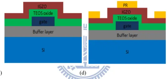
2.1 Device Fabrication and Process Flow
In this section, we introduce the fabrication of the devices. The device structure is the conventional inverted-staggered back-gated TFT. First, we grew a thermal oxide layer of 5000 Å on the Si substrate. Then we deposited Al-Si-Cu of 3000 Å by using physical vapor deposition (PVD) as the gate electrode (Fig. 2.2 (a)). After defining the gate pattern, plasma enhanced chemical vapor deposition (PECVD) was used to deposit TEOS oxide as the gate insulator (Fig. 2.2 (b)). By using an RF sputter, an a-IGZO film was deposited as the channel layer (Fig. 2.2 (c)). A photoresist pattern was then generated with a standard lithographic process to define the source and drain regions (S/D) (Fig. 2.2 (d)). DC sputter was used to deposit a 3000 Å Al layer as the S/D electrodes by lift-off process (Fig. 2.2 (e)). The deposition power was fixed at 100 W and the working pressure was 1 mTorr with Ar flow rate fixed at 12 sccm (Table 2.2) (sccm denotes cubic centimeter per minute at STP). After the photoresist was spin coated on the device (Fig. 2.2 (f)) and exposed by DUV (Fig. 2.2 (g)), HCl:H2O=1:200 solution was used to define the active region (AA) (Fig. 2.2 (h)) . Finally, the
gate contact region was opened by BOE:H2O=1:0 solution. After we scrapped the PR, the
device was completed as shown in Fig. 2.2 (i).
The IGZO target we used was with the atomic ratio In:Ga:Zn:O=1:1:1:4. Here we have different channel deposition conditions with varying oxygen deposition rate. Devices with different channel thickness were also fabricated. The system’s working pressure was around 5 mTorr and the background Ar flow rate was fixed at 50 sccm. A change in the deposition power will change the deposition rate. In this study we choose rf power of 100 W as the
11
deposition condition of the IGZO film based on the experience revealed in reference [47]. Four different oxygen flow conditions, namely, 0, 1, 3, 5 sccm, corresponding to oxygen partial pressure of 0, 1X10⁻⁴, 3X10⁻⁴, 5X10⁻⁴ Torr, respectively, were used and the channel thickness was fixed at 15 nm for studying the effect of oxygen flow rate. The overall channel deposition conditions are summarized in Table 2.1. Effect of oxygen flow on the deposition rate is shown in (Fig. 2.1 (b)). Three different channel thicknesses, namely, 10, 15 and 20 nm, were targeted with fixed oxygen flow rate at 1 sccm for studying the effect of different channel thickness. TFTs with a channel composed of double active layers, which were deposited under different oxygen flow rate, as shown in (Fig. 2.2 (j)), were also fabricated and characterized. We defined the layer near the gate electrode as the 1st layer and the other one the 2nd layer. Four different oxygen flow conditions were used, namely, 1/3, 3/1, 1/5 and 5/1 sccm for the 1st/2nd channel layers, and the thickness of each layer is 7.5 nm in order to fix the total thickness at 15 nm. a-IGZO TFTs with gate dielectric thickness of 10 or 50 nm. The S/D metal deposition was done by either e-gun or sputter For studying the effect of the surrounding ambient, we expose the devices to atmosphere as long as 3 months, and compare them with the devices after 30 mins vacuum annealing. For the study of the effect of stressing and light, ±10 V gate voltage stressing and light exposure ranging 0 ~ 1000 s was applied on some of the devices. Finally, the temperature dependent effect was measured from 25 ℃ to 125 ℃.
12
2.2 Measurement Setup
In all of our study, the measurement of devices was executed by an HP4156A precision semiconductor parameter analyzer for Id-Vg and Id-Vd curves, and by an HP4284 precision
LCR meter for CV curves.
Basic electrical parameters of the fabricated devices were extracted from the electrical characteristics. The threshold voltage (Vth) was extrapolated from Id-Vg curve which was
defined as the gate voltage corresponding to a fixed drain current at 10-6 A under Vd of 0.1 V.
The subthreshold swing (SS) was calculated by the following equation
SS= ( ) , (Eq.2-1) where the minimum SS value was extracted in region when ID is between 10-9 A to
10-11 A. And the mobility (μ) was calculated by the following equation μFE=
‧
‧ ‧ , (Eq.2-2)
where gm was also calculated from Id-Vg curve.
We’ve also extracted the gate voltage-dependent series resistance (Rs) by using the method propose by Hagyoul Bae [21] and Sungwook Park et al.[22-23]. Figs. 2.3 (a)~ (d) show the equivalent circuit model [23]. First, we measured the capacitance with various frequencies and obtained Rm and Cm in Fig. 2.3 (a) . Fig. 2.4 [21] is the measurement results of multi-frequency CV curves and the calculated results of Gm (inset) from Eq. 2.3 where Dm was the dissipation factor:
G = = wC D , (Eq.2-3) Then we calculated Z2 from the measurement results of Rm and Cm (Fig. 2.3 (a) ) using
the following equation:
Z =
( ) − ( ) , (Eq.2-4)
13
[23]) and the Rs-vs.-voltage curve can be plotted as shown in Fig. 2.5 [23].
Furthermore, in order to obtain the density of states (DOS) of defects in the gap, should be calculated with the following procedure:
First, we calculate Z4 in Fig. 2.3 (b) with the following expression:
Z = Rs +
( ) − jw( ( ) + ), (Eq.2-5)
where Rch and Cch are the channel resistance and channel capacitance, respectively. By
comparing the real (A) and the imaginary (B) parts of impedance in Eq. 2.4 and Eq. 2.5, we can obtain Eq. 2.6 and Eq. 2.7
A =
( ) − = ( ), (Eq.2-6)
B =
( ) − Rs = ( ), (Eq.2-7)
Then Rch are obtained with the following equations
= C R , (Eq.2-8) R = {1 + ( ) }B, (Eq.2-9) Then Cch can be calculated by using two frequencies from Eq. 2.10
C = ( ) ( ) ( ) ( ) , (Eq.2-10) After obtaining Rch and Cch, Gp and Gp/w can also be calculated:
G = =
{ ( ) }, (Eq.2-11)
=
( ), (Eq.2-12)
Finally, we can calculate CLOC from the maximum value of ω as shown in Fig. 2.6 [21]
with ωτ = 1. CFREE can be further obtained with the following relation:
C = C −
14
(Eq.2-13)
where CLOC and CFREE represent the capacitance components due to trapping/detrapping of
localized electrons and free electrons, respectively (Fig. 2.3 (e) [21]). Here we simply define the energy level in the gap corresponding to the gate voltage at a specific current, say, 10-13 A, as “E1” and the surface band bending was calculated from the following equation
Φs= ∫ 1 −CCg
ox dV, (Eq.2-14) Finally, the DOS (denoted as g ) can be calculated from the following equation:
g (E) = ( )
15
Chapter 3
Results and Discussion
3.1
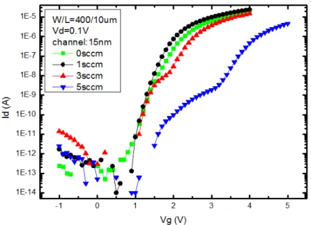
Effects of Deposition Oxygen Flow
Effects of the deposition oxygen flow had been studied previously [24-26] and known to greatly affect the electrical performance of TFTs. Some of those studies reported devices with transfer characteristics showing a hump phenomenon [47], but none of them explained the cause for the observation. In this work, effects of the oxygen flow are also explored. We deposited the channel layer with various oxygen flow rates which are 0, 1, 3 and 5 sccm, respectively. In addition to studying the basic electrical characteristics, we’ve also observed the hump phenomenon and attempted to understand its origin. Figs. 3.1 (a)-(d) show the variation of the transfer characteristics of a-IGZO devices with channel prepared with oxygen flow at 0 sccm, 1sccm, 3 sccm, and 5 sccm, respectively. As we can see from these figures, the variation of the transfer characteristics is the smallest at deposition O2 flow rate of 1 sccm
and getting worse with either increasing or decreasing the deposition oxygen flow.
In Fig. 3.2, the mean transfer curves of a-IGZO devices selected from Figs. 3.1 (a) ~ (d) with channels prepared with different O2 flow rate are shown and compared. The Vth
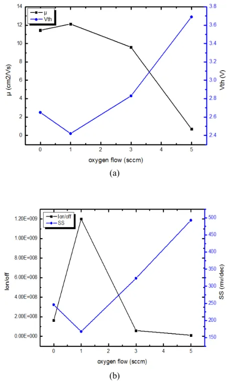
(subthreshold swing, SS) are 2.65 (246), 2.42 (167.7), 2.83 (323.3) and 3.69 V (492.6 mV/dec) for devices with O2 flow of 0, 1, 3, 5 sccm, respectively. On/Off ratios are in the range from
107 to 109 and mobilities are 11.45, 12.13, 9.6 and 0.69 cm2/Vs for O2 flow at 0, 1, 3, 5 sccm,
respectively. The Vth shifts positively as O2 flow increases from 1 to 5 sccm or decreases
from 1 to 0 sccm. The mobility (μ), SS and Ion/off ratio are shown as a function of O2 in Figs.
3.3 (a)-(b). From the above results, we conclude that the condition with O2 flow of 1 sccm is
16
Since the oxygen vacancies are found to act as the shallow donor states for AOS materials, the higher O2 flow rate during deposition will compensate the oxygen vacancies,
and accordingly reduce the free carriers and lower the conductivity of the channel layer [24-26]. This trend explains the increase with increasing O2 flow rate shown above. This can
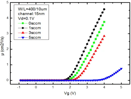
also be proved by the voltage dependent mobility and series resistance (Rs) shown in Figs. 3.4 (a) and (b), respectively, which are extracted based on the method reported in [22-23]. It is seen that the mobility decreases while the Rs increases rapidly as we increase oxygen flow from 1 sccm to 5 sccm. This is due to the higher amount of free carriers in the channel layer when deposition oxygen flow is less. However, the trend is not obvious in the range of O2
flow from 0 to 1 sccm. This might be related to the huge variation in device performance for the case with zero O2 flow.
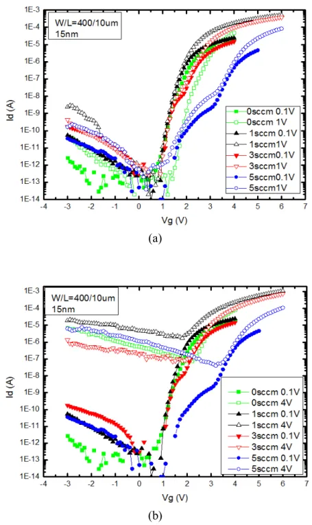
Figs. 3.5 (a)-(b) show the comparison of two transfer characteristics measured at (a) Vd=0.1, 1 V and (b) Vd=1, 4 V. An increase in Vd will boost the on current and the Vth shift is
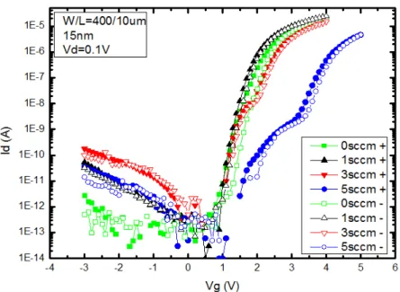
not significant when we increase the drain voltage. The tremendous increase in the off current at Vd of 4 V is due to the gate leakage current (analysis not shown). Fig 3.6 shows the transfer
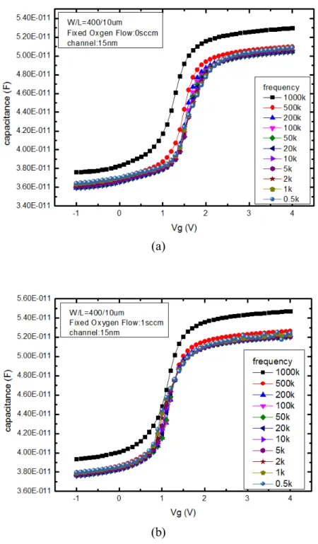
characteristics measured by positive and negative voltage sweeping and the Vth shift is not obviously, either. Also the measured C-V characteristics with multi-frequency for the four splits are shown in Figs. 3.7 (a)-(b) and 3.8 (a), (b), respectively. Fig. 3.9 shows the frequency independent Cg calculated from the procedure introduced in Chap. 2 [21-23]. Here we notice that in Fig. 3.2 the transfer curves show a hump in the subthreshold region when the oxygen flow is 3 sccm or 5 sccm. Here we use the modified conductance method (MCM) proposed by Bae et al.[21] mentioned in Sect. 2.2 to extract the DOS shown in Fig 3.10. We define an energy level as E1 in the gap corresponding to the gate voltage at a specific Id of 10-11 A.
We find that the DOS of defects in the gap is generally much higher in the 3 and 5 sccm splits than the other two. This explains why the SS is worse for the two splits with high O2
17
flow. Moreover, one or two peaks in the defect distribution are observed for these samples. As the surface potential is modulated by the gate bias so as to switch the device to the ON state, the induced electrons have to fill these states first. When the Fermi level moves through the region close to a DOS peak, the abundant defects will slow down the modulation of surface potential with increasing gate bias. This is believed to be the origin for the observed “hump” in the subthreshold region of the two splits with high O2 flow of 3 sccm and 5 sccm.
Finally, Figs. 3.11 (a)-(d) show the output characteristics of devices with O2 flow of 0, 1,
3, and 5 sccm, respectively.
3.2
Effects of Active Layer Thickness
Effects of channel thickness have also been studied by many groups previously [27-31]. TFTs with different channel thickness were studied here, too. Figs. 3.12 (a)-(c) show the transfer characteristics of several a-IGZO devices with channel thickness of 10 nm, 15 nm, and 20 nm, respectively. As we can see from these figures, the variation of the transfer characteristics is comparable among the three splits, although it seems to be a little worse as the channel is thinner. This might be due to the influence of the back channel surface which is expected to be more pronounced as the channel is thinned down.
Typical transfer curves of different splits are shown in Figs. 3.13(a) and (b). The Vth (subthreshold swing, SS) are 5.12 (305), 4.59 (409), and 3.3 V (430 mV/dec) for channel thickness of 10, 15, and 20 nm respectively. On/Off ratios are in the range between 107~108 and mobilities are 8.12, 10.9, and 11.22 cm2/Vs for channel thickness at 10, 15, 20 nm, respectively. These parameters are shown as a function of the channel thickness in Figs. 3.14 (a) and (b).
As we can see from the Id-Vg curves (Fig. 3.13 (a)), the differences of the on current
18
the off current, on/off ratio, SS, mobility, and threshold voltage are all thickness dependent, as shown in Figs. 14 (a) and (b). Increasing the channel thickness would draw a higher off current and worse SS since it is harder to fully deplete the channel layer.
Fig 3.15 (a) shows the mobility with respect to gate voltage for the three splits [22-23]. In Figs. 3.14 (a) and 3.15 (a), we can find the mobility is higher for the device with a thicker channel. This can be explained by percolation conduction theory [12]. The random distribution of Ga3+ and Zn2+ will form potential barriers and the barriers are overcome when the carrier concentration is sufficiently large (~1019 cm-3), thus the mobility increases accordingly. This also reflects on the series resistance (Rs) which was extracted by the method proposed in [22-23], as shown in Fig. 3.15 (b). The Rs starts to decrease at a higher Vg for the device with a thinner channel due to its lower mobility and reduced amount of
carriers. Fig. 3.13 (b) also shows the comparison of transfer characteristics of the devices with different channel thickness at Vd=0.1 and 1 V. We can see that the on current is apparently
improved without worsening the off current.
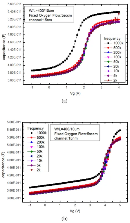
The measured C-V characteristics with multi-frequency are shown in Figs. 3.16 (a)-(c). Fig. 3.17 shows the frequency-independent Cg [21-23] where the difference in the voltage as Cg begins to increase, reflecting the shift in Vth with different channel thickness. Finally, Figs. 3.18 (a)-(c) show the output characteristics of the devices with channel thickness of (a) 10 nm (b) 15 nm (c) 20 nm.
19
3.3
Effects of Surroundings Ambient
AOS materials are very sensitive to surrounding ambient. The devices we fabricated and characterized have no passivation layer in order to study the effect of the surrounding ambient.
The component of air includes oxygen and water vapor. Impacts of these species have been studied by Jin-Seong Park [25] and Kang et al. [26]. As we can see in Fig. 3.19, after exposure to humidity surroundings the Vth shifts negatively accompanied with a dramatic increase in the off-state leakage current by about 103 ~104 times [25]. Fig. 3.20 (a) shows the transfer characteristic of a device measured with different air partial pressure [26]. They found that the Vth shifts positively as the air partial pressure increases. A similar trend is also observed as the ambient is switched to pure oxygen, as shown in Fig. 3.20 (b) [26]. These observations can be explained by the figures shown in Figs. 3.21 (a) and (b). The adsorption of O2 near the back surface, as shown in Fig. 3.21 (a) will tend to attract electrons in the
channel as stated by the following equation:
O + e → O ( ), (Eq.3-1) and then form a depletion layer underneath the adsorption layer, causing the positive Vth shift. In contrast to O2, H2O adsorption, as shown in Fig. 3.21 (b), will donate free electrons to the
channel, causing a negative shift in Vth. Such a phenomenon is also called donor effect [25]. Figs. 3.22 and 3.23 show the transfer characteristics of the fabricated devices with various channel thickness and various O2 flow during the channel deposition, respectively,
measured right after the fabrication and three months later. We find that Vth of almost all splits shifts positively in the two figures as the measurements were done three months later. According to the studies mentioned above [25-26], we conclude that the Vth shift is mainly due to the adsorption of the oxygen molecules from the surrounding atmosphere on the back surface of the devices.
20
In Fig. 3.22, we also notice that the Vth shift caused by adsorbing oxygen is related to the active layer thickness. That is, the thicker the active layer, the harder the oxygen molecules to affect the electrical properties. With the bottom-gate scheme of the fabricated devices, the oxygen molecules would draw more influence on the gated channel conduction as the channel is thinner. In Fig. 3.23, we find that irrespective of the deposition oxygen flow rate, the Vth of all splits shifts positively except for the one with O2 flow of 5 sccm. As have
been pointed out in previous section that the channel layer deposited at 5 sccm is deficient of oxygen vacancies and thus free electrons in the channel. In this case the adsorbed oxygen is harder to take away any of the electrons in the channel, hence the Vth shift isn’t apparent. In Fig. 3.23, the dramatic increase in the off current after 3 months is presumably due to the bad quality of gate dielectric.
3.4
Impacts of Different Gate Dielectric Thickness and Channel Materials
Reduction in gate dielectric thickness is a common method to improve the TFT performance including the SS and on current. This is demonstrated in Fig. 3.24 (a) which shows the transfer characteristics of a-IGZO TFTS with gate dielectric of 10 and 50 nm. The on current and SS are significantly improved with a thinner gate oxide due to the better controllability. This is further evidenced by the data shown in Fig. 3.24 (b) that the mobility increases with gate voltage more rapidly when the gate dielectric is thinner.
So far we know that the thicker channel layer provides more free carriers in the AOS materials as discussed in Sect. 3.2. Based on the presupposition and the fact that ITO is one of the AOS materials which had been commonly used in practical manufacturing of flat-panel display products, we compared the electrical performance of these two materials. Since ITO is more conductive than a-IGZO, we fabricated the ITO TFTs with an ultra-thin active layer of 10 nm and compare their performance with the IGZO TFTs. Fig. 3.25 shows the comparison
21
of the transfer curves of ITO and a-IGZO TFTs. The on current is larger for the ITO TFT but the SS and on/off ratio are better for the a-IGZO TFT. The larger on current displayed by the ITO device is due to the higher concentration of free carriers in the active layer even though the channel thickness is less than that of the a-IGZO film. By the same token, worse off current and SS are also resulted in the ITO one. On the other hand, the better on/off ratio and SS shown by the a-IGZO TFT are due to the better gate controllability.
3.5
Effects of Using Double Active Layer
In order to suppress the off current and improve the on current, double active layer structure was explored in this work (Fig. 2.2 (j)). As has been stated in last chapter that the key parameter investigated in the deposition of the double channel layers is the O2 flow rate.
Fig 3.26 shows the transfer curves of devices with 1st/2nd layer of 1/3, 3/1, 1/5, and 5/1 sccm. Note that the 1st layer is in contact with the gate dielectric, and the thicknesses of both 1st and 2nd layers are 7.5 nm. Also shown in the figure is the control device with the channel prepared by O2 flow rate of 1 sccm. The off currents are the same for all splits but, as compared with
the control device, the on currents are apparently degraded for the devices with double active layer. This indicates that the on performance is majorly dependent on the layer with a higher O2 flow. As mentioned in Section 3.2, the total amount of the free carrier concentration in the
channel is proportional to the channel thickness. The above degraded results associated with the double-layer channel might be due to ultra-thin channel. If the first layer is thickened, expected benefits of the double-layer structure should appear.
22
3.6
Effects of Annealing
In order to resolve the hump phenomenon discussed in Sect. 3.1 and improve the electrical performance, we annealed the devices in the fabrication. Effects of the treatment on the electrical performance are addressed in the section. In Sect 3.3, we speculate that the surrounding oxygen adsorbed on the back surface of the device may cause the Vth shift, thus annealing done in vacuum is explored. The annealing temperature and time are 300 oC and 30 minutes, respectively, done on the devices after fabrication for 3 months.
Fig. 3.27 (a) shows the Id-Vg curves of the devices with various O2 flows measured at
different stages. As indicated previously that after exposing to the air ambient for 3 months, Vth shifts positively apparently. But after the vacuum annealing, Vth shifts negatively. This trend agrees with our speculation that the adsorbed oxygen atoms on the back surface, which cause the positive Vth shift, tend to de-adsorb during the vacuum annealing. We also notice the Vth after annealing is even smaller than the fresh value, as shown in Fig. 3.27 (b). This can be attributed to the fact that some of the oxygen atoms that penetrate into the channel and form weak bonding wherein will be released back to the surrounding [49], causing more oxygen vacancies and thus more free carriers.
Devices with double active channel layers are also examined after vacuum annealing. As mentioned in Sect. 3.5, an obvious hump is observed in some of the as-fabricated samples with double active channel layers. Such a finding is, however, not found and reported in previous studies on devices with double active channel layers [64]. After checking the process sequence, we find that the devices characterized in those previous studies all received thermal annealing. To verify if the annealing is responsible for the disparity, we also performed annealing on some of the devices with double active layer. Here we only compare the devices with channel prepared with O2 flow of 1, 1/3 and 1/5 sccm. Fig 3.28 (a) shows the transfer
23
indeed disappear after the annealing. Moreover, the hysteresis of those devices is not significant. Fig 3.28 (b) and (c) show the transfer characteristics of a-IGZO devices after vacuum annealing for single active layer and double active layer (1/3 and 1/5 sccm) at (b) Vd=0.1V and (c) Vd=4V. The Vth values of the devices become more positively since the
thinner 1st layer with less free carriers. The SS are slightly better for the devices using double active layer and the on current and on/off ratio look fine. For the results with Vd of 4V, the off
current of the device with single active layer apparently increases while it remains low for the devices with double active layer. This is attributed to the use of the 2nd layer which can suppress the back surface leakage current.
3.7
Effects of Bias Stress and Light Stress
Since a-IGZO TFTs are expected to be widely used as the switching transistors in AM-LCD and AMOLED, the devices are usually biased and exposed to light during normal operation. Any issues related to instability caused by bias stress and/or light stress must be crucially treated and resolved. These instability phenomena are typically associated with a shift in Vth and SS degradation. The former is majorly attributed to charge trapping in the gate dielectric and a change in the carrier concentration of the channel film, while the latter is largely caused by the generation of interface states. Light stress could generate electron-hole pairs in the channel and the generated carriers would participate in the process of defect creation inside the devices.
Effects of bias conditions and light exposure on IGZO TFTs have been explored by many groups [54-62]. A number of stress modes, including positive bias stress (PBS), negative bias stress (NBS), light stress (LS), positive bias light stress (PBLS), and negative bias light stress (NBLS), are categorized in the previous works. In this work we also focus on these categories. Figs. 29 (a)~(e) show the results of characterization performed on devices
24
deposited with O2 flow of 1sccm and channel thickness of 10 nm. Fig. 3.29 (a) shows the
effect of PBS. The gate voltage applied to the gate during the stressing is 10 V, while the source and drain are grounded. The Vth shifts positively with increasing stress time and basically no clear degradations on SS and mobility are observed. The rise in leakage current is also seen and has been identified to be due to the gate leakage current, indicating the poor quality of the gate dielectric. The positive shift in Vth is attributed to the electrons trapping in the gate dielectric and a schematic illustration describing the process is shown in Fig 3.30 [60]. Accumulated electrons under the high positive gate bias are trapped in the gate dielectric and cause the positive Vth shift. Fig 3.29 (b) shows the effect of NBS. As can be seen in the figure that there are no apparent Vth shift and SS variation under NBS. The gate voltage applied to the gate during the stressing is -10 V, while the source and drain are grounded. Lacking of holes in the n-type channel of a-IGZO material was considered as the reason for the small influence. However, Nathan et al. [58] found that the Vth shifted negatively under NBS. They attributed this to the de-population of donor-like traps. As the negative bias excludes the electrons away, the empty trap is with positive charge and causing the Vth shift negatively. Fig 3.29 (c) shows the effect of LS. The Vth shift negatively as the light stress time increases. Two possible mechanisms are proposed previously [54-62]. One is the light-induced electron-hole pairs increase the number of free electrons in the channel, thus Vth shifts negatively. Another is that a portion of the holes induced by light are trapped in the gate dielectric, also causing Vth shifts negatively. On the other hand, Chen et al. [59] claimed that the Vth shift is related to the surrounding ambient. They found the Vth shift due to LS is relatively small under oxygen ambient. As mentioned in Sect. 3.3, the adsorbed oxygen atoms will cause a positive Vth shift. However, under the LS, photon-generated e-h pairs will supply the holes to react with the O2- and desorb the oxygen molecules, causing the negative Vth
25
molecules. H2O molecules are also found to induce negative Vth shift as Lee et al. reported in
[55]. Since metastable gap states are generated after H2O molecules are adsorbed, more
electrons induced by light will be captured in these traps, and a negative Vth shift is resulted. Figs. 3.29 (d) and (e) show the effect of PBLS and NBLS, respectively. We notice that the light exposure enhances the Vth shift in the above two cases. For PBLS, the additional electrons generated by the light promote the electron trapping in the gate dielectric . For PBLS, light induced electrons make the turning off of the devices harder, causing Vth shift negatively. On the other hand, for NBLS, light induced holes are attracted by the negative gate bias, leading to a larger negative Vth shift. Trappings of the photon-generated holes are expected to be small due to the fact that the valance band of the oxide semiconductor are mainly composed of 2p oxygen orbitals which cause localization of holes in the channel, thus the negative Vth shift is simply due to the bias physically separating the e-h pairs and reducing the recombination [58]. Fig 3.31 shows the comparison of the transfer characteristics for a-IGZO devices measured under fresh state and after PBS, NBS, LS, PBLS and NBLS. Comparing to the fresh, the SS slightly deteriorates after light illuminating. This are attributed to the conduction of leakage current close to the backside channel/oxide interface which is caused by the light exposure. Fig 3.32 shows the comparison of the voltage dependent mobility of the a-IGZO devices after subjecting to PBS, NBS, LS, PBLS and NBLS. Notice that the mobility obviously decreases at the on state after light exposure.
Fig 3.33 shows the transfer characteristics of a-IGZO devices with channel thickness of 20 nm under (a) PBS and (b) NBS, respectively. Akin to Figs. 3.29 (a) and (b), Vth shift is still positive under PBS while no obvious Vth shift under NBS is observed. However, the Vth shift is smaller in the device with a thicker channel. This may also be attributed to the adsorption and desorption competition of oxygen molecules on the surface of the IGZO channel: Owing to the thicker film, the impact of the surface condition would have less
26
influence on the channel conduction. Fig. 3.34 shows the comparison of transfer characteristics of a-IGZO devices with channel thickness of 20 nm among samples subjecting to PBS, NBS, LS, PBLS and NBLS for 300 s. As compared with the results shown in Fig. 3.31, more apparent stretch-outs in subthreshold region under LS, PBLS and NBLS are observed. We attribute this to the fact that the controllability of the gate bias on the back surface (or the top surface of the channel) declines as the channel becomes thicker [56].
27
Chapter 4
Conclusion
In this thesis, we have successfully fabricated a-IGZO TFTs deposited under various sputtering conditions. With different oxygen flow but fixed channel thickness, the Vth increases with increasing deposition oxygen flow, accompanying with mobility lowering. This is attributed to the decrease in oxygen vacancies which donate the free carriers. Also, an anomalous hump phenomenon is observed under a high deposition oxygen flow. Films with fixed deposition oxygen flow but different channel thickness were also fabricated and characterized in order to study the effect of the channel thickness. We found that the Vth shifts negatively as we increase the channel thickness. With a fixed deposition oxygen flow, since the population of free carriers is more in the thicker channel, the a-IGZO TFTs are harder to turn off accordingly.
For the reliability issues, we examine the effects of the surrounding ambient on the a-IGZO TFTs. Oxygen molecules are verified to cause the negative Vth shift when the devices are exposed to the air after 3 months. This is attributed to the adsorbed oxygen molecules which act as the electron traps and reduce the overall free carriers in the channel.
In order to improve the electrical performance, a-IGZO TFTs with a double active layer were also fabricated. With this scheme, we successfully suppress the leakage current while sustain the same SS, on current and on/off ratio.
Vacuum annealing was used for solving the hump phenomenon and balancing the effects of surrounding ambient. By the desorption of the oxygen molecules and the breaking of the weak oxygen bonds in the channel, oxygen vacancies and free electrons both increase. The anomalous lowering in mobility may be due to the phonon scattering.
28
Since a-IGZO TFTs are used as the switching transistors in AM-LCD and AMOLED, and often exposed to light while under biased during operation, the associated reliability issues are essential. In this study, the instability of positive bias stress (PBS), negative bias stress (NBS), light stress (LS), positive bias light stress (PBLS) and negative bias light stress (NBLS) with different channel thickness are addressed. Vth shifts positively with PBS since the electrons are trapped in the gate dielectric during the stressing. Due to the fact that a-IGZO is an n-type material, the shift in Vth is negligible under NBS. Light induced electron-hole pairs are found to enhance the PBS and NBS. A stretch out phenomenon is also observed for devices with a thicker channel under LS, which is attributed to the adsorption of oxygen molecules.
29
References
[1] E. Fortunato, P. Barquinha, and R. Martins, “Oxide semiconductor thin-film transistors: A review of recent advances,” Advanced Material, vol. 24, no 22, pp. 2945-2986, June 2012.
[2] M. Lto, M. Kon, C. Miyazaki, N. Lkeda, M. Ishizaki, R. Matsubara, Y. Ugajin, and N. Sekine, “Amorphous oxide TFT and their applications in electronic displays,” Physica
Status solidi (a), vol. 205, no 8, pp. 1885-1894, August 2008.
[3] T. Kamiya, and H. Hosono, “Material characteristics and applications of transparent amorphous oxide semiconductors,” npg asia materials, vol. 2, pp.15-22, May 2010. [4] J. Y. Kwon, D. J. Lee, and K. B. Kim, “Review paper: transparent amorphous oxide
semiconductor thin film transistor,” Electronic Materials Letters, vol. 7, no.1, pp. 1-11, March 2011.
[5] K. Momura, A. Takagi, T. Kamiya, H. Ohta, M. Hirano, and H. Hosono, “Amorphous oxide semiconductor for high-performance flexible thin-film transistors,” Japanese
Journal of Applied Physics, vol. 45, no 5B, pp. 4303-4308, May 2006.
[6] J. S. Park, W. J. Marng, H. S. Kim, and J. S. Park, “Review of recent development in amorphous oxide semiconductor thin-film transistor devices,” Thin Solid Films, vol. 520, no. 6, pp.1679-1693, January 2012.
[7] M. J. Powell, “The physics of amorphous-silicon thin-film transistors,” IEEE
Transaction on Electron Devices, vol. 36, no. 12, pp.2753-2763, December 1989.
[8] T. Kamuya, K. Nomura, and H. Hosono, “Present status of amorphous In-Ga-Zn-O thin-film transistors,” Science and Technology of Advanced Material, vol. 11, no. 4, August 2010.
[9] P.K. Weimer, proceeding of the institute of radio engineers, 50, 1462, 1962. [10] P.K. Weimer, presented at IRE-AICE Device Res. Conf., Standford, CA, 1961.
30
[11] R. L. Hoffman, “ZnO-channel thin-film transistors: mobility,” Journal of Applied
Physics, vol. 95, no. 10, pp. 5813-5819, May 2004.
[12] K. Nomura, H. Ohta, A. Takagi, T. Kamiya, M. Hirano, and H. Hosono, “Room-temperature fabrication of transparent flexible thin-film transistors using amorphous oxide semiconductors,” Nature, vol. 432, no. 23, pp.488-492, July 2004. [13] T. W. Yen, “Fabrication and characterization of a-IGZO Thin Film Transistors,”
master’s thesis, Dept. Electronics Engineering & Inst. of Electronic, NCTU, 2011.
[14] A. Takagi, K. Nomura, H. Ohta, H. Yangi, T. Kamiya, M. Hirano, and H. Hosono, “Carrier transport and electronic structure in amorphous oxide semiconductor, a-InGaZnO4,” Thin Solid Films, vol. 486, no. 1-2, pp. 38-41, August 2005.
[15] T. C. Fung, C. S. Chuang, C. Chen, K. Abe, H. Kumomi, and J. Kanicki, “2-D numerical simulation of high performance amorphous In-Ga-Zn-O TFTs for flat panel displays,”
AM-FPD’12, Tokyo , July 2008.
[16] K. Jeon, C. Kim, I. Song, J. Park, and S. Kim, “Modeling of amorphous InGaZnO thin-film transistors based on the density of states extracted from the optical response of capacitance-voltage characteristics,” Applied Physics Letters, vol. 93, no. 18, pp. 182102-182103, November 2008.
[17] M. Kimura, T. Nakanishi, K. Nomura, T. Kamiya, and H. Hosono, “Trap densities in amorphous-InGaZnO4 thin-film transistors,” Applied Physics Letters, vol. 92, pp.
133512-133513, March 2008.
[18] H. H. Hsiehm, T. Kamiya, K. Nomura, H. Hosono, and C.C. Wu, “Modeling of amorphous InGaZnO4 thin film transistors and their subgap density of states,” Applied
Physics Letters, vol. 92, no.13, pp.133503, April 2008.
[19] A. Hino, S. Morita, S. Yasuno, T. Kishi, K. Hayashi, and T. Kugimiya, “Electronic structure in amorphous In-Ga-Zn-O metal-oxide-semiconductor diodes with various gate
![Fig. 1.4 Comparison of the DOS between a-Si:H and a-IGZO films. [3]](https://thumb-ap.123doks.com/thumbv2/9libinfo/7495761.115835/54.892.171.756.125.758/fig-comparison-dos-si-h-igzo-films.webp)