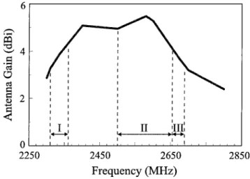
bands I, II, and III, the measured axial ratios are less than 1.2, 1.8, and 2.3 dB, respectively (see Table I). Measured radiation patterns at the center frequencies of bands I, II, and III are also plotted in Figure 4, and good CP radiation has been obtained. Figure 5 shows the measured antenna gain for the proposed antenna. For band I, the measured antenna gain is about 3.2– 4.3 dBic. For bands II and III, the measured antenna gain is about 4.0 –5.5 dBic and 3.3– 4.0 dBic, respectively.
4. CONCLUSION
A low-profile broadband PQHA with good CP radiation charac-teristics has been proposed and successfully implemented. The proposed antenna shows a very wide CP bandwidth of larger than
27%, which covers the frequency bands of 2310 –2360 MHz, 2500 –2655 MHz, and 2655–2690 MHz for broadcasting satellite applications. In addition, the proposed antenna has a low profile of only 27.2 mm, and good antenna gain has also been obtained. REFERENCES
1. J.C. Louvigne and A. Sharaiha, Synthesis of printed quadrifilar helical antenna, Electron Lett 37 (2001), 271–272.
2. S. Licul and A.A. Chatzipetros, Folded helix antenna design, U.S. Patent No. 6229499 B1, May 2001.
3. J.C. Louvigne and A. Sharaiha, Broadband tapered quadrifilar helical antenna, Electron Lett 37 (2001), 932–933.
4. United States Frequency Allocations, Office of Spectrum Management, National Telecommunications and Information Administration, U.S. Department of Commerce.
© 2003 Wiley Periodicals, Inc.
A 1.2-V FULLY INTEGRATED 2.4-GHz
LOW-NOISE AMPLIFIER IN 0.35-
m
CMOS TECHNOLOGY
C. C. Meng,1M. H. Chiang,2and T. H. Wu2
1Department of Communication Engineering
National Chiao Tung University
HsinChu 30056, Taiwan, Republic of China
2Department of Electrical Engineering
National Chung-Hsing University Taichung, Taiwan, Republic of China
Received 10 July 2002
ABSTRACT: A 1.2-V fully integrated 0.35-m inductively degenerated
common source CMOS low-noise amplifier has been demonstrated at 2.4 GHz in this paper. A simple common source configuration can be operated at lower voltage and has lower output impedance when compared with a conventional high output impedance cascode LNA circuit topology. The input matching inductance, output matching inductance, and source degen-eration inductance are integrated on a single chip. The fully integrated 2.4-GHz CMOS LNA has 5.27-dB power gain, 17-dB input return loss, 15-dB output return loss, 4-dB noise figure, and⫺1-dBm IIP1dBand 8-dBm IIP3at Vdd⫽ 1.2 V and Idd⫽ 10 mA, respectively. © 2003 Wiley Periodicals, Inc.
Microwave Opt Technol Lett 36: 136–139, 2003; Published online in Wiley InterScience (www.interscience.wiley.com). DOI 10.1002/mop.10699 Key words: CMOS; LNA; MOSFET amplifier
Figure 3 Measured axial ratio in the broadside direction of the proposed antenna
Figure 4 Measured radiation patterns at the center frequencies of (a) band I (2310 –2360 MHz), (b) band II (2500 –2655 MHz), and (c) band III (2655–2690 MHz) for the proposed antenna
Figure 5 Measured antenna gain for the proposed antenna
INTRODUCTION
A low-noise amplifier is the key element of an RF receiver. There is a strong effort toward highly integrated, and thus low-cost, radio frequency integrated circuits in wireless communication systems. CMOS apparently has the lowest cost among all the semiconductor technologies for wireless communication. The 0.35-m CMOS process is fabricated by the inexpensive I-line photolithography techniques instead of expensive deep-UV, and even phase-shift, mask photolithography techniques which are used for gate length 0.25m and below. Generally speaking, inductors, resistors, and
capacitors limit the size of an RFIC, and thus smaller-gate-length CMOS technology does not improve RFIC chip size. Recently, a highly integrated CMOS transceiver for Bluetooth applications has been implemented in a digital 0.35-mm CMOS process [1]. How-ever, most of the CMOS LNAs implemented still use off-chip matching elements to reduce chip size and provide tuning flexi-bility [1–3]. There are some works on fully integrated CMOS cascode LNAs [4 –7]. A cascode CMOS LNA has better isolation and is the most popular LNA topology. On the other hand, a simple inductively degenerated common source LNA can operate at lower voltage and could have smaller on-chip inductances. The larger input capacitance caused by the Miller effect and the lower output impedance of a simple inductively degenerated common-source LNA require smaller input gate resonant inductance and smaller drain inductance for impedance transformation to 50⍀. In this paper, a 1.2-V fully integrated inductively degenerated common-source CMOS LNA is demonstrated at 2.4 GHz by using 0.35-m digital CMOS technology. The experimental results show that the CMOS LNA has 5.27 dB gain and 4 dB noise figure at Vdd⫽ 1.2
V and Idd ⫽ 10 mA. On the other hand, the CMOS LNA has
6.12-dB gain and 4-dB noise figure at Vdd⫽ 3.3 V and Idd⫽ 10
mA.
CIRCUIT DESIGN
A simple common-source CMOS LNA schematic is illustrated in Figure 1. Lg and Ld are the input matching inductance and the
output matching inductance, respectively, while the two parallel L1
and L2shown in Figure 1 are the source degenerated inductances.
L-type matching networks are used at both input and output. The
design approach for this CMOS LNA is a measurement-based Figure 1 Schematic of the inductively degenerated CMOS LNA.
Figure 2 Photo of the fabricated CMOS LNA. [Color figure can be viewed in the online issue, which is available at www.interscience.wiley.com.]
design, which is very accurate but requires a test run to generate a circuit-element database. High frequency measurements were per-formed on different device sizes and various inductors after the test run was made. The low-noise amplifier is then simulated by the measured S-parameters. The inductors used in the CMOS LNA design are 5 turns (260m ⫻ 280 m) for Lg, 4 turns (235m ⫻
250m) for Ld, and 2 turns (150m ⫻ 175 m) for L1and L2,
respectively. A multi-finger CMOS device is used to reduce the gate resistance for better power gain and noise figure. The CMOS device has 0.35-m gate length and eight fingers with 25-m-unit gate width. The photo of the fabricated CMOS LNA is shown in Figure 2. The low noise amplifier is implemented with a 0.35-m digital CMOS technology.
EXPERIMENTAL RESULTS
The measurement-based design approach is indeed a useful RFIC design method. Simulation results and measured results of the CMOS LNA agree very well. Because the CMOS LNA can be operated at 1.2 V supply voltage and thus rf performance are measured at both 1.2 V and 3.3 V supply voltages when Idd⫽ 10
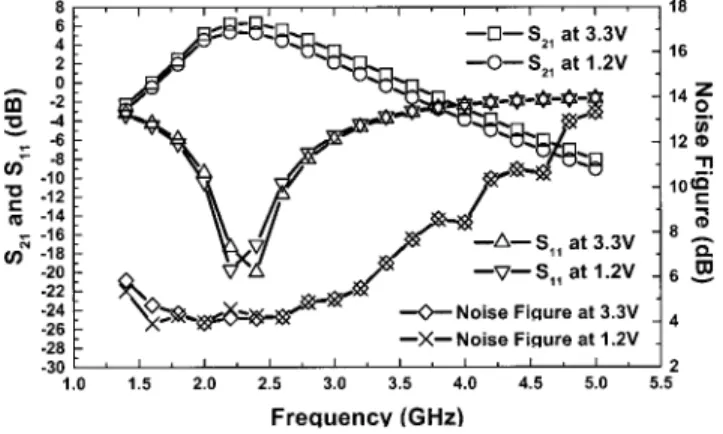
mA. The measured small signal rf results are illustrated in Figures 3 and 4. Figure 3 illustrates S21(forward transmission), S11(input return loss), and noise figure; while Figure 4 illustrates S22(output return loss) and S12(reversed transmission). S21is 6.31 dB, S11is ⫺20 dB, S12is⫺29 dB, S22is⫺17 dB and NF ⫽ 4 dB at 2.4 GHz
when Vdd⫽ 3.3 V. The noise figure shown here indicates that the
noise figure is at its best around 2.4 GHz. Large signal gain
compression and two tone intermodulation were also measured and shown in Figure 5. As shown in Figure 5, IP1dBis 3 dBm and IIP3is 16 dBm at 3.3 V. When the CMOS LNA is operated at 1.2 V, S21is 5.27 dB, S11is⫺17 dB, S12is⫺28 dB, S22is⫺15 dB, and NF⫽ 4 dB at 2.4 GHz. IP1dBis⫺1 dBm and IIP3is 8 dBm at 1.2 supply voltage.
DISCUSSION AND CONCLUSION
A low-voltage (1.2 V) truly fully integrated CMOS LNA was demonstrated in a simple common source configuration. Power gain can be increased by cascading two identical common-source CMOS LNAs. The noise figure of a cascaded amplifier is calcu-lated by the well-known equation NF⫽ NF1⫹ (NF2⫺ 1)/G1. If the LNA in this letter is in cascade, the total noise figure is 4.71 (or 4.57) dB and gain is 10.54 (or 12.62) dB at Vdd⫽ 1.2 (or 3.3)
V and Idd⫽ 20 mA. A cascading common source LNA can be a
fair comparison to a cascode LNA, because a cascode LNA is a two-stage amplifier (CS-CG configuration). The noise figure of the LNA is not very good and is probably due to the inadequate gate finger number and unit gate width. Power gain can possibly be improved by using smaller a unit-gate width and more gate fingers [7]. In conclusion, a fully integrated 2.4-GHz CMOS LNA with 5.27-dB power gain, 17-dB input return loss, 15-dB output return loss, 4-dB noise figure, and⫺1-dBm IIP1dBand 8-dBm IIP3 is demonstrated at Vdd ⫽ 1.2 V and Idd⫽ 10 mA.
ACKNOWLEDGMENT
This work is supported by National Science Council (Contract number: NSC 90-2213-E-005-001) and Ministry of Education of Taiwan, Republic of China (Contract number: 89-E-FA06-2-4). REFERENCES
1. H. Darabi, S. Khorram, H.M. Chien, M.A. Pan, S. Wu, S. Moloudi, J.C. Leete, J.J. Rael, M. Syed, R. Lee, B. Ibrahim, M. Rofougaran, and A. Rofougaran, A 2.4-GHz CMOS transceiver for Bluetooth, IEEE J Solid-State Circuits 36 (2001), 2016 –2024.
2. D.K. Shaeffer and T.H. Lee, A 1.5-V, 1.5-GHz CMOS low noise amplifier, IEEE J Solid-State Circuits 32 (1997), 745–759.
3. E. Abou-Allan, J.J. Nisbet, and M.C. Maliepaard, Low-voltage 1.9-GHz front-end receiver in 0.5-m CMOS technology, IEEE J Solid-State Circuits 36 (2001), 1434 –1443.
4. C.S. Kim, M. Park, C.H. Kim, Y.C. Hyeon, H.K. Yu, K. Lee, K.S. Nam, A fully integrated 1.9-GHz CMOS low-noise amplifier, IEEE Micro-wave Guided Wave Lett 8 (1998), 293–295.
5. C.J. Debono, F. Maloberti and J. Micallef, A 1.8 GHz CMOS low noise Figure 3 Measured S21, S11 and noise figure of the 0.35m CMOS
LNA at both 1.2 V and 3.3 V supply voltage when Idd⫽ 10 mA.
Figure 4 Measured S22and S12of the 0.35m CMOS LNA at both 1.2
V and 3.3 V supply voltage when Idd⫽ 10 mA.
Figure 5 Measured IP1dBand IIP3of the 0.35m CMOS LNA at both
1.2 V and 3.3 V supply voltage when Idd⫽ 10 mA.
amplifier, the 8th IEEE Int Conf Electronics, Circuits Syst 3 (2001), 1111–1114.
6. R.A. Rafla and M.N. El-Gamal, Design of a 1.5 V CMOS integrated 3 GHz LNA, Proc 1999 IEEE Int Symposium Circuits Systems 2 (1999), 440 – 443.
7. E.H. Westerwick, A 5-GHz CMOS low noise amplifier with a 2.5 dB noise figure, 2001 Int Symposium VLSI Tech, Syst Appl, pp 224 –227. © 2003 Wiley Periodicals, Inc.
ANALYSIS OF CONFORMAL ANTENNAS
ON A COMPLEX PLATFORM
Jian Liu and Jian-Ming Jin
Center for Computational Electromagnetics Department of Electrical and Computer Engineering University of Illinois at Urbana-Champaign
Urbana, Illinois 61801-2991
Received 28 June 2002
ABSTRACT: A numerical technique is presented for characterizing the
radiation patterns and mutual coupling of conformal antennas mounted on a complex platform. This technique uses the higher-order finite ele-ment method (FEM) to model the antennas and the platform and em-ploys the boundary integral equation to terminate the FEM computa-tional domain. The resulting numerical system is solved using a novel preconditioner in conjunction with the multilevel fast multipole algo-rithm for the fast evaluation of boundary integrals. © 2003 Wiley
Peri-odicals, Inc. Microwave Opt Technol Lett 36: 139 –142, 2003; Published online in Wiley InterScience (www.interscience.wiley.com). DOI 10.1002/mop.10700
Key words: conformal antennas; finite element method; numerical
anal-ysis; radiation
1. INTRODUCTION
Modern aircraft are usually equipped with many antennas for a variety of communication, detection, tracking, and surveillance purposes. To reduce the radar signature and adverse effects on the aerodynamic design, antennas are often conformal to the surface of the vehicle and sometimes embedded in a layered dielectric medium. Placing these antennas on aircraft inevitably introduces distortion in their radiation patterns and causes mutual coupling. The distortion in the radiation patterns may reduce the desired coverage for effective communica-tions and compromise accuracy of isolating and locating targets. The
existence of mutual coupling, caused by space waves, surface waves, and scattering by the platform, reduces the electromagnetic isolation between the antennas and consequently makes it difficult to operate the antennas simultaneously. Therefore, it is important to develop accurate numerical prediction tools to characterize the radiation pat-terns and mutual coupling of the antennas mounted on a complex, often large, platform.
Because of the high complexity of the problem, limited work has been carried out in the past. In [1], a technique is presented for calculating the radiation pattern of a microstrip patch antenna on a cylindrical body using a three-dimensional (3D) finite element method (FEM) to analyze the patch antenna and a two-dimensional (2D) method of moments (MoM) to characterize the effect of the cylindrical body. Its application is limited to predicting the radia-tion patterns of patch antennas on 2D bodies. In [2] and [3], the FEM is combined with a high-frequency asymptotic method to predict the radiation patterns of conformal antennas on a 3D platform. Again, the FEM is used to analyze the antennas and the asymptotic method is employed to characterize the effect of the platform on the radiation patterns. Since the asymptotic methods are not capable of modeling surface waves and near-field scatter-ing accurately, this hybrid method cannot accurately simulate the mutual coupling of the antennas. To accurately predict the radia-tion patterns and simulate the mutual coupling of the antennas on a platform, it is necessary to use a first principle method, such as the FEM and MoM or their hybridization, to carry out the analysis. Such an analysis is, however, very difficult because of the com-plexity of the structures and the large size of the platform.
In this paper, we present a novel hybrid technique, which is our first attempt to deal with this complex problem. This technique is based on a recently developed finite element– boundary integral (FE– BI) method [4]. It employs higher-order vector elements to accurately model complex geometries and reduce the number of unknowns for large-size problems and incorporates a highly effective preconditioner [5] to accelerate the convergence of the iteration solution of the FE–BI system and the multilevel fast multipole algorithm (MLFMA) [6] to speed up the evaluation of boundary integrals.
Figure 1 Conformal antennas embedded in a dielectric medium situated on a large platform
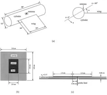
Figure 2 (a) Patch antenna mounted on a cylinder with a wing; (b) top view of the patch antenna; (c) longitudinal section view of the patch antenna
![Figure 2 Photo of the fabricated CMOS LNA. [Color figure can be viewed in the online issue, which is available at www.interscience.wiley.com.]](https://thumb-ap.123doks.com/thumbv2/9libinfo/7490649.115034/2.945.101.448.59.336/figure-photo-fabricated-color-figure-viewed-available-interscience.webp)