國 立 交 通 大 學
電信工程研究所
碩 士 論 文
應用於
IEEE 802.11 無線區域網路之
高線性度轉導電容式連續濾波器
High linearity Transconductance-C Continuous-Time Filter
for IEEE 802.11 Wireless Local Area Networks
研究生:許新傑
指導教授:洪崇智 博士
應用於
IEEE 802.11 無線區域網路之
高線性度轉導電容式連續濾波器
High linearity Transconductance-C Continuous-Time Filter
for IEEE 802.11 Wireless Local Area Networks
研 究 生:許新傑 Student:Shin-Jye Hsu
指導教授:洪崇智 Advisor:Prof. Chung-Chih Hung
國 立 交 通 大 學 電 信 工 程 研 究 所 碩 士 論 文
A Thesis
Submitted to Institute of Communication Engineering College of Electrical Engineering and Computer Science
National Chiao Tung University In Partial Fulfillment of the Requirements
For the Degree of Master
In
Communication Engineering September 2009
Hsinchu, Taiwan, Republic of China
應用於
IEEE 802.11 無線區域網路之
高線性度轉導電容式連續濾波器
學生: 許新傑 指導教授: 洪崇智
國立交通大學
電信工程研究所
摘 要
本論文提出兩種改善轉導放大器線性度的技術,目的是用來製作高線性度的 轉導電容式濾波器。濾波器的用途主要應用於IEEE 802.11 無線區域網路。採用 轉導電容式濾波器的原因是因為,轉導電容式濾波器比起交換電容濾波器以及主 動電阻電容濾波器更適合用在高速的系統上。但是對於轉導放大器而言,線性度 較差是主要的缺點,所以如何改善線性度變成一個很重要的課題。 第一種轉導放大器的電路是根據源極衰減電路的架構,並結合電壓跟隨器與 輸入衰減器來達到高線性度。利用所提出的轉導放大器當作基本組件,用來實現 一個截止頻寬為 40MHz的四階線性相位低通濾波器。此濾波器是以台積電0.18-μm CMOS製程來設計,所佔的面積為 0.510×0.500mm2。在輸入訊號 10MHz振幅為 0.8Vpp時,其第三諧波失真約為-53.4dB。在輸入訊號 39MHz及 41MHz時,其第 三內調變失真約為-36dB。在供應電壓為 1.8V時,功率消耗為 14.1mW。 第二種轉導放大器的電路也是根據源極衰減電路的架構,並結合超級源極隨 耦器與正回饋迴路來降低非理想效應的影響。此轉導放大器不僅可以達到高線性 度,而且還可以對抗製程的變異。在輸入訊號 10MHz振幅為 0.6Vpp時,其第三 諧波失真約為-69dB,並且其第三諧波失真直到 25MHz時至少為-57dB。在輸入訊號9MHz及 11MHz時,其第三內調變失真約為-60dB。此轉導放大器是以台積
電0.18-μm CMOS製程來製造,所佔的面積為 0.145×0.134mm2。在供應電壓為
High linearity Transconductance-C Continuous-Time Filter
for IEEE 802.11 Wireless Local Area Networks
Student: Shin-Jye Hsu Advisor: Dr. Chung-Chih Hung
Institute of Communication Engineering
National Chiao Tung University
Hsinchu, Taiwan
ABSTRACT
In this thesis, two linearity enhancement techniques for transconductor to implement the transconductance-C filter are proposed. The main application is for IEEE 802.11 wireless local area networks. For high frequency applications, the transconductance-C filters are more suitable than switched-capacitor filters and active RC filters. Nevertheless, the main drawback of the transconductor is poor linearity, so to improve the linearity is a significant topic.
The first transconductor circuit is based on the source degeneration structure, and combines the flipped voltage follower with input attenuators to achieve high linearity. By using the proposed OTA as a building block, a 4th order equiripple linear phase lowpass filter with the cutoff frequency of 40MHz is implemented. The filter is designed in the TSMC 0.18-μm CMOS process technology and occupies an area of 0.510×0.500mm2. The third-order harmonic distortion (HD3) is about -53.4dB with 10MHz 0.8Vpp input signal. The third-order inter-modulation (IM3) is about -36dB by
the two-tone measurement of 39MHz and 41MHz. The power consumption is 14.1mW under a 1.8V supply voltage.
The second transconductor circuit is also based on the source degeneration structure, and combines the super source follower with a positive feedback to alleviate the non-ideal effects. The OTA can not only achieve high linearity performance but also be against the process variation. The linearity of the OTA is about -69dB HD3 at 10MHz and still below -57dB at frequency up to 25MHz for a 0.6-Vpp differential
input. Two tone inter-modulation shows about -60dB at 9 MHz and 11MHz. The OTA fabricated in the TSMC 0.18-μm CMOS process technology occupies a small area of 0.145×0.134mm2. For 1.8-V supply voltage, the static power consumption is 2.22mW.
誌
謝
隨著這份碩士論文的完成,兩年來在交大的求學生涯也跟著告一個段落,往 後迎接著我的,又是另一段嶄新的人生旅程。本論文得以順利完成,最先要感謝 的,當然是我的指導教授洪崇智老師。這兩年的研究生涯中,給予我無微不至的 指導與照顧,且讓我在研究主題上有無限的發展空間。而類比積體電路實驗室所 提供完備的軟硬體資源,讓我在短短兩年碩士班研究中,學習到如何開始設計類 比積體電路,乃至於量測電路,甚至單獨面對及思考問題的所在。此外要感謝闕 河鳴教授和溫宏斌教授撥冗擔任我的口試委員並提供寶貴意見,使得本論文更為 完整。也感謝國家晶片系統設計中心提供先進的半導體製程,讓我有機會將所設 計的電路加以實現並完成驗證。 另一方面,要感謝所有類比積體電路實驗室的成員兩年來的互相照顧與扶 持。首先,感謝博士班的學長薛文弘、周芳鼎、廖德文和陳家敏以及已畢業的碩 士班學長林永洲、楊文霖、夏竹煒和郭智龍在研究上所給予我的幫助與鼓勵。特 別是文弘學長,由於他平時不吝惜的賜教與量測晶片時給予的幫助,使得我的論 文研究得以順利完成,對於他的無私幫助,我沒齒難忘。另外我要感謝李尚勳、 簡兆良和黃聖文等諸位同窗,透過平日與你們的切磋討論,使我不論在課業上, 或研究上都得到了不少收穫。尤其是工四 718 實驗室的同學們,兩年來陪我ㄧ起 努力奮鬥,一起渡過那段同甘共苦的日子,也因為你們,讓我的碩士班生活更加 多采多姿,增添許多快樂與充實的回憶。此外也感謝學弟們李人維、許凱修、林 均曄、陳伽維、蘇俊仁、蔡湯唯和鄭世東的熱情支持,因為你們的加入,讓實驗 室注入一股新的活力與朝氣,我祝你們研究順利。 到這邊,特別要致上最深的感謝給我的父母及家人們,感謝你們從小到大所 給予我的栽培、照顧與鼓勵,讓我得以無後顧之憂地完成學業,朝自己的理想邁 進,我要謝謝你們給我那麼多的愛和付出,我會一輩子記在心理。 最後,所有關心我、愛護我和曾經幫助過我的人,願我在未來的人生能有一 絲的榮耀歸予你們,謝謝你們。 許新傑 于 交通大學工程四館 718 實驗室 2009.9.16
Table of Content
Table of content
Chapter 1 Introduction………...1
1.1 Motivation………...1 1.2 Analog Filter………...2 1.3 Thesis Overview………..4Chapter 2 Operational Transconductance Amplifiers……….5
2.1 Introduction………5
2.2 Basic Structures of High-linearity OTAs………5
2.2.1 Differential Input………5
2.2.2 Pseudo-differential Input………7
2.2.3 Source Degeneration………..8
2.2.4 Flipped Voltage Follower……….10
2.2.5 Super Source Follower……….11
2.3 Linearity-improved OTAs……….11
2.3.1 Source Degeneration with OPAMPs………11
2.3.2 Source Degeneration with a Positive Feedback………...12
Chapter 3 Proposed OTAs for High Linearity Applications……14
3.1 Introduction………..14
3.2 Proposed Flipped Voltage Follower with Input Attenuator…………..…14
3.2.1 Characteristics and Operation of the OTA circuit………...14
Table of Content
3.2.3 Noise Analysis………17
3.3 Proposed Super Source Follower OTA with a Positive Feedback………18
3.3.1 Characteristics and Operation of the OTA circuit………18
3.3.2 Non-ideality analysis………20
3.3.3 Noise Analysis………..20
3.4 Common Mode Feedback Circuit……….21
Chapter 4 Transconductance-C Filters………...24
4.1 Introduction………..24
4.2 Elementary Transconductor Building Blocks………..24
4.2.1 Resistors………..25
4.2.2 Integrators……….26
4.2.3 Gyrators………27
4.3 Fourth-order Equiripple Linear Phase Low-pass Filter……….30
4.3.1 Biquad Section……….30
4.3.2 Filter Architecture………32
4.3.3 Output Buffers……….33
Chapter 5 Simulation and Experimental Results………..36
5.1 Introduction………..36
5.2 Performance of Flipped Voltage Follower OTA with Input Attenuators..39
5.2.1 Simulation Results of the Transcondutor……….39
5.2.2 Simulation Results of the Filter………41
Table of Content
5.3 Performance of Super Source Follower OTA with a Positive Feedback..47
5.3.1 Simulation Results of the Transcondutor……….47
5.3.2 Measurement Results of the Transcondutor……….50
Chapter 6 Conclusions………..53
6.1 Conclusions………..53
6.2 Future Works……….53
List of Figures
List of Figures
Fig. 2.1 the Differential Pair………...6
Fig. 2.2 the Pseudo-Differential Pair………..7
Fig. 2.3 the Concept of Common Mode Feedforward Circuit………...8
Fig. 2.4 the Source Degeneration Pair………9
Fig. 2.5 the Flipped Voltage Follower………..10
Fig. 2.6 the Super Source Follower………..11
Fig. 2.7 Improving the Linearity of a Fixed Transconductor by Using OPAMPs……12
Fig. 2.8 Source-degenerated Differential Pair with a Positive Feedback……….12
Fig. 3.1 Modified Flipped Voltage Follower with Input Attenuators………...15
Fig. 3.2 Super Source Follower OTA with a Positive Feedback………..18
Fig. 3.3 the Simple Differential Amplifier………...21
Fig. 3.4 the High-gain Differential Pair………..22
Fig. 3.5 the Common Mode Feedback Circuit for Both Proposed OTA……….22
Fig. 4.1 Resistor Simulates with Transconductors………..25
Fig. 4.2 the Grounded Inductor Implemented by a Gyrator………26
Fig. 4.3 the Floating Inductor Realized by a Capacitor between Two Gyrators…….27
Fig. 4.4 the Single-ended Integrator………27
Fig. 4.5 the Fully Differential Integrators………27
Fig. 4.6 the Non-ideal Single-ended Integrator………29
Fig. 4.7 Gain and Phase Response of the Integrator………29
Fig. 4.8 the 2nd Order Bandpass Filter for Passive RLC Prototype………..31
Fig. 4.9 the 2nd Order Bandpass and Lowpass Filter for Active Gm-C Prototype…...31
Fig. 4.10 the 4th Order Equiripple Linear Phase Lowpass Filter.……….32
Fig. 4.11 the Output Buffer Using Transconductor-based Resistor……….34
Fig. 4.12 the Output Buffer Using Source Follower………35
Fig. 5.1 (a) Magnitude Response (b) Phase Response……….39
Fig. 5.2 the Common Mode Rejection Ratio………...40
Fig. 5.3 the Power Supply Rejection Ratio………..40
Fig. 5.4 the Tuning Range of the OTA……….40
Fig. 5.5 the OTA Tuning Range with Highest and Lowest Vtune………..41
Fig. 5.6 the Total Harmonic Distortion………41
Fig. 5.7 (a) Magnitude Response (b) Group Delay………..42
List of Figures
Fig. 5.9 the Inter-modulation Distortion………..43
Fig. 5.10 (a) the Layout (b) the Die Photo………..44
Fig. 5.11 (a) Magnitude Response (b) Group Delay………45
Fig. 5.12 the Total Harmonic Distortion………..46
Fig. 5.13 the Inter-modulation Distortion………46
Fig. 5.14 (a) Magnitude Response (b) Phase Response………..47
Fig. 5.15 the Common Mode Rejection Ratio……….48
Fig. 5.16 the Power Supply Rejection Ratio………48
Fig. 5.17 the Tuning Range of the OTA………..48
Fig. 5.18 the OTA Tuning Range with Highest and Lowest Vtune………49
Fig. 5.19 the Total Harmonic Distortion………..49
Fig. 5.20 (a) the Layout (b) the Die Photo………..50
Fig. 5.21 the Total Harmonic Distortion………..51
Fig. 5.22 the Inter-modulation Distortion………51
List of Tables
List of Tables
TABLE 4.1 Denominator of Biquad Section………..33
TABLE 5.1 the Specification of Filter……….43
TABLE 5.2 the Specification of the OTA………49
Chapter 1
Introduction
1.1 Motivation
With the progressing of the technology, the wireless communication systems become more and more popular. In wireless applications, the channel selection filter, which is between the down-conversion mixer and the analog-to-digital converter, is an essential component for direct conversion receiver. Recent demand for multi-standard transceivers uses the direct-conversion structure owing to the high integration of a single chip and the ease of system design. In recent years, the high-performance high-linearity filters are required for the wireless local area networks (WLANs).
The standard of IEEE 802.11 is one of the protocols for the wireless local area networks. The bandwidths of intermediate-frequency (IF) filtering for IEEE 802.11 are as follows, IEEE 802.11a/g (10MHz), IEEE 802.11b (12MHz), IEEE 802.11n (20MHz) [1]. To achieve the stable communication systems with low distortion, the linearity of the channel selection filters is a critical factor. In addition, future trends pushing toward higher data rates will require higher frequency ranges with equal or better linearity.
There are several amendments for IEEE 802.11 such as 802.11a/b/g/n. First of all, the 802.11a operates in the 5.4GHz, which is using relatively unused 5GHz band, as an advantage. However, high carrier frequency also brings a disadvantage: The effective overall range of 802.11a is less than that of 802.11b/g. Second, 802.11b and 802.11g devices operate in the 2.4GHz band, which is heavily used by other applications, suffer interference from microwave ovens, cordless telephones and
Bluetooth devices. Moreover, 802.11b/g use the direct sequence spread spectrum signaling (DSSS) and orthogonal frequency division multiplexing (OFDM) methods, respectively. Finally, 802.11n is enhanced by adding multiple-input multiple-output (MIMO) and many other newer features.
1.2 Analog Filters
In modern communication systems, using analog filters to reduce the noise is in common. In general, analog filters include passive filters and active filters. The passive filter is composed of resistors, capacitors and inductors. For example, LC-ladder is one of the useful topologies, because it is insensitive to device variation. However, passive elements occupy more areas and thus increase cost in integrated circuits. Therefore, active filter is proposed to resolve the shortcoming. In recent decades, the development of active filters progress rapidly. There are many methods to implement the active filter. In CMOS technologies, the analog filter design techniques can be divided into analog sampled-data techniques and time continuous techniques.
Sampled-data filter are implement by using several non-overlapping clock. The clock frequency and capacitor ratios can determine the characteristics of switched capacitor filters. A major advantage is the highly accuracy of its integrator time constant. Nevertheless, switched capacitor filters will be limited in their application range from about 10Hz to about 1MHz. This phenomenon is mainly due to the finite bandwidth of the OPAMP, finite resistance of the switches and the clock feed-through. Usually, the OPAMP has to be fast enough to settle to the right output level within half a clock period. Furthermore, for 0.1% settling precision, the settling time should be higher than the GBW of the OPAMP at least by a factor of 7. Therefore, switched capacitor filter is difficult to implement in high frequency applications. Finally, it
should be mentioned that sampled-data filters need an anti-aliasing continuous-time filter to band-limit the frequencies of the input signal.
In the past, the continuous-time filters were developed as complementary of switched capacitor filters as anti-aliasing and smoothing filters. Nowadays, time continuous techniques are an alternative in low-frequency applications. Moreover, these techniques allow the integration of filters to operate from 1MHz to several hundreds of MHz. Continuous-time filters can deal with the analog signal without sampling, so they do not need pre-filtering and post-filtering to prevent aliasing problems. However, the precision of these filters is the major disadvantage. For the design of high-performance CMOS active filters, namely, active RC filters, MOSFET-C filters and OTA based filters. The active RC filters consist of OPAMP, resistors and capacitors. The resistors usually implemented by poly-silicon. However, the variation of the resistors and capacitors has great influence on RC filters. In general, the active RC filters are suitable for low-frequency applications. The MOSFET-C filters are based on the active RC filters. The resistors of active RC filters are substituted for the CMOS, which is operated in triode region. One major drawback of this approach is the distortion. Moreover, the operating frequency of the filters is limited due to using the OPAMPs. Consequently, The MOSFET-C filters are not suitable for high-frequency applications. The operational transconductance amplifier-capacitor (OTA-C) filters, also called Gm-C filters, offer many advantages over other continuous-time filters. The major advantages are low power consumption and high-frequency capability. Nevertheless, due to the openloop operation, Gm-C filters generally perform poorly as far as linearity is concerned. The relatively high distortion of Gm-C filters reduces their range of applications.
1.3 Thesis Overview
Chapter 2 demonstrates some basic structures of OTAs operating with high linearity. It describes the advantages and disadvantages of these structure as well as its characteristics. Furthermore, some linearity-improved circuits are also presented in this chapter.
Chapter 3 demonstrates the proposed OTAs, which modify the basic structures to enhance the linearity. First, we discuss the operating mechanism of the OTAs, and then utilize the mathematical equations to verify the concept. Finally, the noise analysis of the OTAs is discussed.
Chapter 4 present the principle of the Gm-C filters. Furthermore, output buffers are also discussed.
In chapter 5, the simulation results and experimental results are presented. Chapter 6 makes the conclusion to this work.
Chapter 2
Operational Transconductance Amplifiers
2.1 Introduction
Operational transconductance amplifier (OTA) is one key building block in continuous-time integrated filters. In high-frequency continuous-time filters, Gm-C filters have often been employed since OTAs provide high Gm’s and a good controllability. However, the main disadvantage of a Gm-C structure is the poor linearity caused by the openloop operation. Therefore, the linearity is a critical topic to enhance. In recent years, several techniques for improving the linearity of CMOS OTA have been proposed [2]-[6].
In the design of OTAs, the transconductance should be tuned for compensation for process tolerances and temperature variation without degrading the entire circuit performance. Moreover, with the progressing of the CMOS technology, short channel effect is another obstacle to resolve.
2.2 Basic Structures of High-linearity OTAs
In this section, we introduce several basic structures of OTA. For instance, a fully differential structure is used to suppress common-mode noise, even-order distortions and power supply noise.
2.2.1 Differential Input
One approach to maintain a constant transconductance is to apply a differential pair, as shown in Fig. 2.1.
Fig. 2.1 the Differential Pair
As M1 and M2 operate in the saturation region, the output current I1 and I2 are expressed as 2 2 , 1 1 2 , 1 1 ( ) 2 1 thn x i V V V I =
β
− −(2.1) 2 2 , 1 2 2 , 1 2 ( ) 2 1 thn x i V V V I = β − −
(2.2) As a result, the output differential current can be obtained by subtracting equation (2.2) from the equation (2.1) as
)
)(
(
1 2 1,2 2 , 1 2 1 i i cm x thn oI
I
V
V
V
V
V
I
=
−
=
β
−
−
−
(2.3)where the value Vcm is the input common mode voltage, and it is fixed to a constant
DC level. Also, the Vx can be described as
B I B x I V β 2 = (2.4)
From the equation (2.3), the transconductance is proportion toβ1,2(Vcm−Vx−Vthn1,2). The transconductance of the differential pair is constant if the Vx remains constant.
However, in practice, the Vx varies with the process and the variation of input signal.
Consequently, keeping Vx constant is one of the solutions to improve the linearity. In
addition, according to the equation (2.4), tuning the tail current can adjust Vx to obtain
2.2.2 Pseudo-differential Input
Another approach is a pseudo-differential pair, which removes the tail current from the differential pair, as shown in Fig. 2.2. The pseudo-differential pair alleviates the influence caused by the variation of Vx. As a result, the linearity can be improved.
Moreover, the voltage headroom of the pseudo-differential pair is larger than the differential pair. Therefore, the pseudo-differential pair is adequate for low-voltage applications.
Fig. 2.2 the Pseudo-Differential Pair
The analyses of the pseudo-differential pair are as follow. Assuming the two transistors are operating in the saturation region, the output current I1 and I2 are described as 2 2 , 1 1 2 , 1 1
(
)
2
1
thn iV
V
I
=
β
−
(2.5) 2 2 , 1 2 2 , 1 2 ( ) 2 1 thn i V V I =β
− (2.6) The output differential current is given by)
)(
(
1 2 1,2 2 , 1 2 1 i i cm thn oI
I
V
V
V
V
I
=
−
=
β
−
−
(2.7)As we can see, the output differential current is a linear function without the factor Vx.
Although the pseudo-differential pair has better linearity and larger headroom than the differential pair, the former also has several shortcomings. First, the tuning of transconductance is limited. Although tuning the body voltage [5] can vary the threshold voltage to adjust the transconductance, the tuning range of body voltage
should be restricted to avoid large leakage current. Second, the common mode gain increases without the tail current. The common mode rejection ratio (CMRR) is about 0dB. Therefore, the pseudo-differential pair requires extra circuit, common mode feedforward (CMFF), to increase the CMRR.
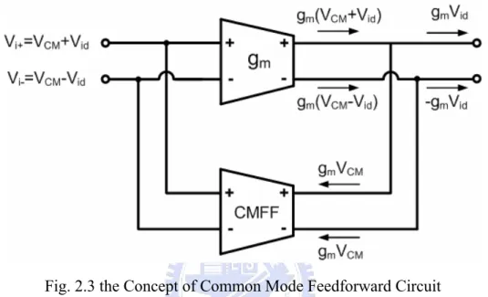
The concept of the common mode feedforward circuit is shown in Fig. 2.3 [7].
Fig. 2.3 the Concept of Common Mode Feedforward Circuit
The CMFF circuit generates the common mode current of output. The differential mode current will remain by cancelling the common mode current of output, which implies that the common mode signal would not be amplified. As a result, the CMRR increases.
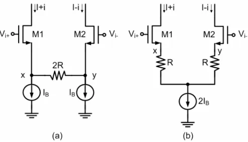
2.2.3 Source Degeneration
A source degeneration structure is one popular method to implement the OTA. The circuit is shown in Fig. 2.4.
Fig. 2.4 the Source Degeneration Pair
The ideal operation of the source degeneration pair is that Vi+ and Vi- perfectly
follow to the ends of the resister. Thus, the voltage across the resister generates the output current. The voltage-to-current conversion is extremely linear. However, the impedance between the gate and the source of the two transistors are not zero, and the impedance varies with the transconductance of M1 and M2. Therefore, the linearity of the source degeneration pair is degraded.
As shown in [8], the voltage-to-current conversion is given by
id n n B ox n sat DS id
v
N
L
W
I
C
V
N
v
i
)
1
2
(
)
)
1
(
2
(
1
2 ) (+
×
+
−
=
μ
(2.8) N N R Gm + = 1 1 (2.9) From the equation (2.9), the transconductance is proportional to the factor 1/R, so increasing the resistor can decrease the transconductance. By using Taylor Series, the third order harmonic distortion (HD3) can be derived as2 ) ( 2 3 ( ) 32 1 ) 1 1 ( sat DS id V v N HD × × + = (2.10)
increasing the transconductance or the value R, which means increasing the factor N, can improve the HD3.
Although the voltage-to-current conversions are the same in Fig. 2.4(a) and Fig. 2.4(b), the circuits have different properties. For Fig. 2.4(a), the tail currents contribute differential noise to the output, which is a dominant noise in the circuit. For Fig. 2.4(b), the voltage drop on the resistors reduces the range of the input common mode voltage.
2.2.4 Flipped Voltage Follower
In recent years, a flipped voltage follower is one popular approach for low-voltage low-power circuit design, including the OTA design. The circuit is shown in Fig. 2.5 [9].
Fig. 2.5 the Flipped Voltage Follower
Unlike the conventional voltage follower, the circuit in Fig. 2.5 is able to sink a large amount of current. However, the current source limits the sourcing capability. The large sinking capability is due to the low impedance at the output node. By analyzing the circuit, we can derive the output impedance
approximately, where 1 2 1 / 1 m m o o g g r r = mi
transistor Mi, respectively.
2.2.5 Super Source Follower
A super source follower, Fig. 2.6, shows another method of implementing a linear OTA.
Fig. 2.6 the Super Source Follower
The properties of the super source follower are as follow. The output impedance of the super source follower is the same order as the flipped voltage follower, which is
approximately . Moreover, to acquire a correct operation point for the
transistors M1 and M2, the condition I
1 2 1 / 1 m m o o g g r r =
B1>IB2 must be satisfied.
2.3 Linearity-improved OTAs
With the issue of the linearity becomes more and more significant, the linearity enhancement techniques are presented recently. In this section, we discuss two enhancement techniques, which have already been proposed.
2.3.1 Source Degeneration with OPAMPs
As discussion in subsection 2.2.3, the linearity degrades since the input voltages do not perfectly follow to the ends of the resistors. The idea to alleviate this phenomenon is using the operational amplifiers. The circuit is shown in Fig. 2.7.
Fig. 2.7 Improving the Linearity of a Fixed Transconductor by Using OPAMPs The virtual ground in each operational amplifier forces the source voltage of M1 and M2 to equal those of Vi+ and Vi-. Therefore, the input voltage appears directly across
resistor and does not depend on the Vgs voltages of M1and M2, which obtains better
linearity than the conventional circuits.
2.3.2 Source Degeneration with a Positive Feedback
Fig. 2.8 shows a source-degenerated differential pair with a positive feedback gm-boosting circuit [10].
Fig. 2.8 Source-degenerated Differential Pair with a Positive Feedback
The main boosting circuit consists of transistors M2 and M3, with gm of
the positive feedback loop reduces the high source resistance to 50Ω. The approximate expression is as 2 1
1
1
m m sg
g
R
=
−
(2.11) where gmi is the transconductance of transistor Mi. The smaller the resisters Rs are,Chapter 3
Proposed OTAs for High Linearity Applications
3.1 Introduction
As mentioned in chapter 2, the main shortcoming of the OTAs is the poor linearity. Chapter 2 also presents some structures and techniques to enhance linearity. However, it is not good enough for some applications. Therefore, we propose two modified circuits to acquire better linearity performance in this chapter. The two circuits are both based on the source degeneration structure and adding extra concepts to implement. Besides, the common mode feedback circuit, which is necessary for the fully differential circuits, is also presented in this chapter.
3.2 Proposed Flipped Voltage Follower with Input Attenuators
In this section, the linearity enhancement technique which combines the flipped voltage follower with source degeneration is proposed. The FVF structure has good properties for high linearity OTA design as mentioned in subsection 2.2.4. Moreover, input attenuators are added to achieve larger input range and better linearity.
3.2.1 Characteristics and Operation of the OTA circuit
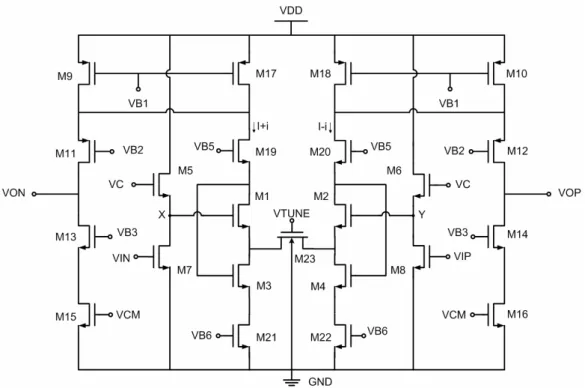
Fig. 3.1 Modified Flipped Voltage Follower with Input Attenuators
The transistors M1~M4 are the FVF structure which implies the source of M1 and M2 are low output impedance. According to this property of the FVF, the relation between input voltages to output current can be expressed as
)
2
(
2 , 1 4 , 3 2 , 1 m o m tune Y xr
g
g
R
i
V
V
−
≅
×
+
(3.1)By comparing with the conventional source degeneration circuit in figure 2.4, which
the voltage-to-current conversion can be described as (2 2 )
2 , 1 m i i g R i V V+− − ≅ × + , we
can identify that the non-ideal effects caused by the nonlinear transconductances can be reduced.
By analyzing the harmonic distortion of the circuit, we discover that the small input signal can obtain good linearity, such as equation (2.10). Therefore, using the transistors M5~M8 as the input attenuators is one approach to execute it. The attenuate ratio is determined by the aspect ratio of transistors, which is given by
5 7 5 7 5 7
)
(
)
(
)
(
2
)
(
2
L
W
L
W
I
L
W
C
I
L
W
C
g
g
V
V
d ox n d ox n m m IN x≅
=
=
μ
μ
(3.2) The larger aspect ratio of M5 and M6 causes the smaller input signal in VX and VY,respectively. From equations (3.1) and (3.2), the transconductance can be derived as
2 , 1 4 , 3 2 , 1 6 , 5 8 , 7
2
)
(
)
(
o m m tune IN IP mr
g
g
R
L
W
L
W
V
V
i
G
+
=
−
=
(3.3)From the equation (3.3), there is a trade-off between the transconductance and the linearity.
In the OTA designs, the tuning circuit is not only used to alleviate the influences resulting from the process and temperature variations, but also applied to implement the multi-band filters. In this case, the transistor M23 operating in the triode region can replace the resistor Rtune, which is given by
(
GS tn)
ox n tuneV
V
L
W
C
R
−
⎟
⎠
⎞
⎜
⎝
⎛
=
μ
1
(3.4)Tuning the gate voltage of M23 can adjust the value of resistor, thereby varying the transconductance. Furthermore, a regulated cascade output stage, the transistors M9~M16, is used to enhance the output resistance.
3.2.2 Non-ideality Analysis
While designing the OTA, a fully differential structure is used to suppress the even-order distortions, ideally. However, the mismatch caused by the process variations is unavoidable. Consequently, the critical paths should be designed carefully.
linearity. In addition, it also impacts the value of the transconductance directly. Second, the mismatch caused by the current mirror leads to the even-order distortion. In other words, the precise current mirror can alleviate the distortion. Finally, the body effect should be taken into consideration for the distortion.
In figure 3.1, M1~M8 are the input pair and the layout should be symmetry for low even-order distortion. Furthermore, by connecting the bulk and source terminals together, the body effect would be minimized.
3.2.3 Noise Analysis
In the communication systems, the noise is a critical issue for transmitting the signal. While designing the devices, the noise should be taken into consideration to ensure that the signal can be transmitted correctly. The device electronic noise is separated into two different types: the flicker noise and the thermal noise. The flicker noise, also called 1/f noise, is the dominant noise when the frequency is less than the corner frequency. On the contrary, the dominant noise is the thermal noise.
Since flicker noise is related to the level of DC, if the current is kept low, thermal noise will be the predominant effect. The thermal noise can be modeled by a current source connected between the drain and the source with a special density as:
m
n
kT
g
I
2=
4
δ
(3.5) where k is the Boltzmann constant, T is the absolute temperature, gm is the source
conductance, and the device noise parameter δ depends on the bias condition. We
have defined , where n equals to the odd number (ex: ).
Thus, the thermal noise density evaluated at the output node is derived as
) 1 ( ) (n
=
m n+ mg
g
g
m1=
g
m2(
)
(
)
(
)
⎪
⎪
⎪
⎭
⎪⎪
⎪
⎬
⎫
⎪
⎪
⎪
⎩
⎪⎪
⎪
⎨
⎧
⎟⎟
⎠
⎞
⎜⎜
⎝
⎛
+
×
⎥
⎦
⎤
⎢
⎣
⎡
+
+
⎟
⎠
⎞
⎜
⎝
⎛
+
+
⎥
⎥
⎦
⎤
⎢
⎢
⎣
⎡
+
+
+
⎟⎟
⎠
⎞
⎜⎜
⎝
⎛
+
=
2 2 21 3 1 17 15 9 2 7 5 7 5 2 ,1
1
2
[
8
TUNE m m m TUNE m m m m m m m out nR
R
g
g
g
R
g
g
g
g
g
g
g
kT
I
TUNEδ
δ
δ
δ
(3.6)From the equation (3.6), decreasing the attenuate ratio will cause the additional noise at the output. This is a tradeoff between the linearity and the noise. Also, to reduce the thermal noise, the transconductance of input transistors should be maximized and the transconductance of tail current should be minimized.
3.3 Proposed Super Source Follower OTA with a Positive Feedback
As discussion in subsection 2.3.2, the source degeneration with a positive feedback can obtain low source resistance
2 1 1 1 m m s g g
R = − . However, due to the
process and temperature variations, the transconductance of M1 and M2 does not perfectly match. Therefore, the super source follower with a positive feedback is proposed to alleviate the non-ideal effects and achieves better linearity than conventional one.
3.3.1 Characteristics and Operation of the OTA circuit
The proposed transconductor circuit is shown in Fig. 3.2
The transistors M1~M4 and M5~M8 are the two pairs of super source follower. The negative feedback loops, loop 1~4, make the source of M1, M2, M5 and M6 to be the low impedance nodes. Moreover, with the same aspect ratio of M9~M12, the positive feedback loops, loop 5 and 6, reduce the output impedance of X and Y. The output impedance of X and Y is given by
1 3 1 5 7 5 X
1
1
R
o m m o m mg
r
g
g
r
g
−
≅
(3.7) 2 4 2 6 8 6 Y1
1
R
o m m o m mg
r
g
g
r
g
−
≅
(3.8)This result is derived through several steps. At first, we transfer Fig. 3.2 into small signal model. And then, assuming the body effect is ignored for simplicity. Furthermore, the equations can be expressed by using the Kirchhoff's current law (KCL) and Kirchhoff's voltage law (KVL). Finally, the result is derived from the equations.
The value of RX could approximate to zero by choosing appropriate M1~M8
device dimension. By comparing with equation (2.11), the first and second terms of RX are quite less than RS. Therefore, the mismatch caused by process variation could
be minimized. From the equations (3.7) and (3.8), the transconductance can be presented as Y X total IN IP m
R
R
R
V
V
i
G
+
+
=
−
=
1
(3.9)where Rtotal is the sum of R1, R2 and Rtune. Minimizing the RX can suppress the
nonlinearity to acquire better total harmonic distortion (THD). As mentioned before, tuning the gate voltage of M25 can vary the transconductance.
Although the circuit has six loops, the stability of the circuit is not an issue. The reason is that the output impedance and capacitance are larger than other nodes. As a
result, the dominant pole is located at the output. Because the impedance and intrinsic capacitance of the other nodes are much lower than the output node, the second pole is in high frequency without affecting the stability.
While designing the Gm-C filters, the input and output of OTAs normally connect together. As a result, to confirm the correct common mode voltage is significant. The transistors M13~M16 are the source follower for dc level shifting to assure function work. In addition, the transistors M17~M24 are the output stage.
3.3.2 Non-ideality Analysis
As discussion in subsection 3.2.2, we can suppress the non-ideality effects by using several methods. In figure 3.2, the source followers, M13 and M14, may slightly influence the linearity. Moreover, the bias currents of the super source followers are too vital to neglect. Also, the bulk and source terminals connect together in the critical paths.
3.3.3 Noise Analysis
As discussion in subsection 3.2.3, the thermal noise is the dominant noise in high frequency. Also, we have defined
g
m(n)=
g
m(n+1), where n equals to the odd number(ex: ). As a result, the output-referred noise density of the super source follower OTA with a positive feedback is derived as
2 1 m m
g
g
=
(
)
(
)
(
)
⎪ ⎪ ⎪ ⎭ ⎪⎪ ⎪ ⎬ ⎫ ⎪ ⎪ ⎪ ⎩ ⎪⎪ ⎪ ⎨ ⎧ ⎟⎟ ⎠ ⎞ ⎜⎜ ⎝ ⎛ + × ⎥ ⎦ ⎤ ⎢ ⎣ ⎡ + + ⎟ ⎠ ⎞ ⎜ ⎝ ⎛ + + ⎥ ⎥ ⎦ ⎤ ⎢ ⎢ ⎣ ⎡ + + + + + ⎟⎟ ⎠ ⎞ ⎜⎜ ⎝ ⎛ + = 2 2 1 7 5 23 17 9 3 1 2 13 15 13 2 , 1 1 2 1 [ 8 total mT m m total m m m m m m m m out n R R g g g R g g g g g g g g kT I totalδ
δ
δ
δ
(3.10)where gmT1 is the transconductance of the tail current transistors. From the equation
gain less than unity. The increase in degeneration factor, Rtotal, increases the noise
contribution of the tail current transistors since it is split in an unbalanced way causing differential output noise. Moreover, it can be the most significant noise component for large degeneration factors.
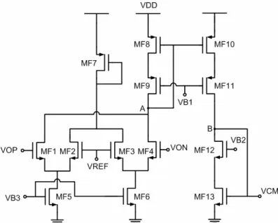
3.4 Common Mode Feedback Circuit
In the filter design, the output of OTA generally connects to the input of next stage OTA. Consequently, the common mode feedback circuit is necessarily needed to obtain the correct input and output common mode voltage of the OTA. The two circuits are presented as below to interpret the necessity of common mode feedback circuit [11].
A simple differential amplifier which the inputs and outputs are short is shown in Fig. 3.3. The common mode voltage of the inputs and output can be easily derived as
2
D SS DD I R
V − .
Fig. 3.3 the Simple Differential Amplifier
The other circuit is shown in Fig. 3.4. In ideality, the currents through M3 and M4 are equivalent to ISS/2. Nevertheless, because of the fabrication process, the
slightly greater than ISS/2, M3 and M4 will operate in the triode region to reduce the
drain current to ISS/2. On the contrary, if ISS/2is slightly greater than ID3,4, M5 will
operate in the triode region to make ISS/2 equal to ID3,4. The non-well defined output
common mode voltage would make the transistors operate in the unwanted regions. Therefore, the common mode feedback circuit is indispensable for the fully differential circuits to fix the output common mode voltage at the expected value.
Fig. 3.4 the High-gain Differential Pair
The CMFB circuit is shown in Fig. 3.5, and the operational mechanisms are described as follows [12].
The input transistors MF1~MF4 is utilized to detect the common mode voltage and compare with the reference voltage. If the common mode of the OTA output signal is equal to the desired voltage VREF, the current through MF8 will keep constant and
thus the voltage VCM is fixed. Nevertheless, the common mode of the OTA output
signal is not the same as VREF all the time. The voltage difference between them is
mirrored through MF8 to vary VCM, thus making the output common mode voltage to
the desired value. For example, if the output common mode voltages are larger than the VREF, the drain current of MF8 will increase. The current mirror also makes the
current through MF10 increase, thereby VCM increasing. In the output stage of Fig.
3.1 and Fig. 3.2, increasing VCM leads to decreasing the output common mode voltage.
This mechanism of negative feedback loop makes the output common mode voltage equal to VREF.
When the OTA operates at high frequency, the CMFB circuit must be stable as well. The open loop gain of the CMFB circuit is
(
L out)
mf B mf A out mf mf out CMFB CMFB R sC g C s g C s R g R s g s A × + ⎟ ⎟ ⎠ ⎞ ⎜ ⎜ ⎝ ⎛ + ⎟ ⎟ ⎠ ⎞ ⎜ ⎜ ⎝ ⎛ + × = × ≅ 1 1 1 ) ( ) ( 13 8 4 , 1 (3.11)where CA and CB are the total capacitance at the points A and B, respectively. From
the equation (3.11), the dominant pole is at 1/(CL×Rout)and the non-dominant poles
are at and . The non-dominant poles should be designed far away
from the unit gain frequency to increase the phase margin of the OTA.
A mf C
Chapter 4
Transconductor-C Filter
4.1 Introduction
As mentioned in the chapter 1, the sampled-data analog filters, the active RC filters and MOSFET-C filters are restricted for high-frequency operation. On the contrary, Gm-C filters are aimed specifically at high-frequency integrated filters. Although high-frequency filters are the main aim of this design method, Gm-C filters also can be used at low frequencies. In this chapter, we will introduce the concepts of Gm-C filters [13].
As the name “Gm-C filters” suggests, we wish to employ only transconductors and capacitors as basic components. The other elementary building blocks, such as resistors, integrators and inductors can be implemented by the transconductors. While designing the Gm-C filters, the first step is choosing an appropriate prototype to satisfy the specification. Moreover, according to the transfer function given by the prototype, we can design the parameters of devices. Finally, the output buffers are added to prevent the degradation caused by loading effects.
4.2 Elementary Transconductor Building Blocks
In this section, we present the methods for using the transconductors to replace the passive elements, such as resistors and inductors. Because the resistors are difficult to implement with sufficient accuracy and over an adequate value, the transconductors are useful to simulate resistors. As for the LC ladders, the transconductors are the convenient approach for building electronic inductors. By reducing the usage of passive elements, the chip areas can be shrunk. At last, we also
investigate the integrators built in Gm-C form.
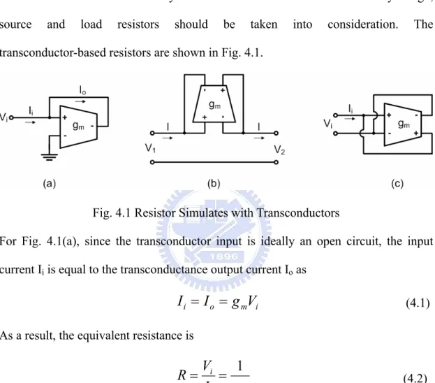
4.2.1 Resistors
In general, there is little need for resistors in the area of Gm-C filters except source and load resistors in doubly terminated LC ladders. For low-sensitivity design, source and load resistors should be taken into consideration. The transconductor-based resistors are shown in Fig. 4.1.
Fig. 4.1 Resistor Simulates with Transconductors
For Fig. 4.1(a), since the transconductor input is ideally an open circuit, the input current Ii is equal to the transconductance output current Io as
i m o
i
I
g
V
I
=
=
(4.1) As a result, the equivalent resistance ism i i
g
I
V
R
=
=
1
(4.2)In Fig. 4.1(b), we connect the two inputs to two different voltages, and feed the outputs back to the inputs. The relation between input currents and output voltage can be described as
)
(
V
1V
2g
I
I
I
i=
o=
=
m−
(4.3)Consequently, the resistor is m
g
I
V
V
R
=
1−
2=
1
(4.4) Observing the results found in Fig. 4.1(a) and Fig. 4.1(b), we know that the negative feedback cause the positive resistors. On the other hand, a negative resistor,m i
i I R g
V =− =−1 , by using the positive feedback is shown in Fig. 4.1(c).
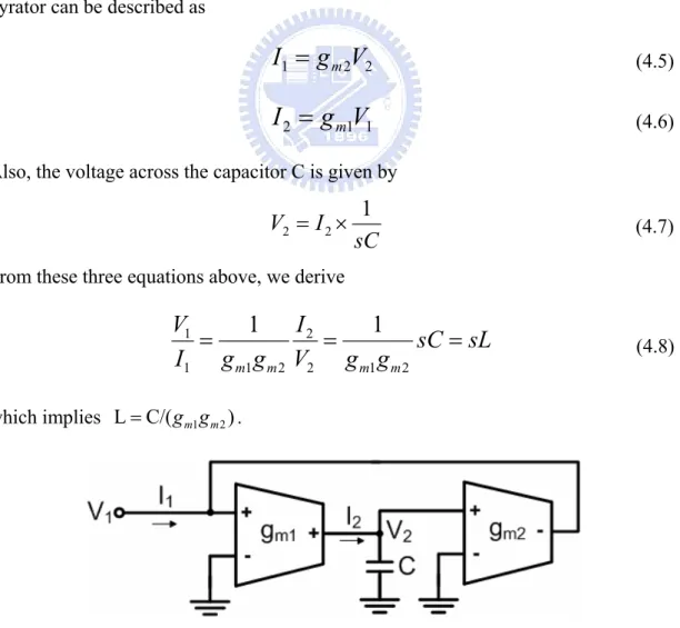
4.2.2 Gyrators
Especially in LC ladders, a gyrator is a useful element because it allows us to convert a capacitor into an inductor, as shown in Fig. 4.2. The characteristic of the gyrator can be described as
2 2 1
g
V
I
=
m (4.5) 1 1 2g
V
I
=
m (4.6) Also, the voltage across the capacitor C is given bysC
I
V
2=
2×
1
(4.7) From these three equations above, we derivesL
sC
g
g
V
I
g
g
I
V
m m m m=
=
=
2 1 2 2 2 1 1 11
1
(4.8) which implies L=C/(gm1 mg 2).Moreover, a floating inductor is presented in Fig. 4.3.
Fig. 4.3 the Floating Inductor Realized by a Capacitor between Two Gyrators
4.2.3 Integrators
In this subsection, we introduce the properties of the integrator, which is the fundamental building block of Gm-C filters. To realize an integrator in Gm technology, a transconductor and a capacitor are used as presented in Fig. 4.4.
Fig. 4.4 the Single-ended Integrator
In most integrated applications, the fully differential circuits are common used because they have better noise immunity and distortion properties. Fig. 4.5 presents the fully differential integrators.
At first, we analyze the integrator in Fig. 4.4 for simplicity. In the ideal case, both the input and output impedance of the transconductor are infinite. The transfer function of the integrator can be derived as
sC g s V s V m i o = = ) ( ) ( H(s) (4.9) On the jω-axis, the equation becomes
)
(
1
)
(
)
(
1
)
H(
ω
ω
ω
ω
ω
j
Y
j
jB
j
G
C
j
g
j
m=
+
=
=
(4.10)From the equation (4.10), we can see that the ideal integrator has infinite DC gain. Besides, quality factor and phase margin are defined as Q(jω)=B(jω) G(jω) and
] ) ( ) ( [ tan 180 1 B jω G jω
PM =− °+ − , respectively. This phenomenon means that the
ideal transconductor has infinite quality factor and PM = 90− ° for all frequencies. Finally, the unity gain frequency for the integrator is
C
g
mT
=
ω
(4.11)As for the non-ideal transconductor, the transfer function includes extra parameters of delay and non-zero conductance G. The delay is caused by the parasitic poles and zeros of transconductor. However, due to the parasitic poles and zeros locating at markedly higher frequency than the unity gain frequency, we could model this circumstance only by one single effective zero. The zero in the right half-plane (RHP) leads to the phase lag. On the other hand, the zero in the left half-plane (LHP) results in the phase lead.
this non-ideal integrator is 1 2 2 nonideal
1
1
1
1
)
(
)
(
(s)
H
τ
τ
τ
s
s
A
g
C
s
s
g
g
s
V
s
V
o o m i o+
−
=
+
−
=
=
(4.12)The non-zero conductance causes finite dominate pole and DC gain which is given by
o m o
g
g
A
g
C
=
=
,
1τ
(4.13)Fig. 4.6 the Non-ideal Single-ended Integrator
In Fig. 4.7, the magnitude and phase response of the integrator is given. Normally,
2
1 1
1τ <<ωT << τ
The parasitic zero and finite DC gain result in the deviation of phase from− 90°. The phase error is defined as
°
+
=
Δ
ϕ
(
j
ω
)
arg[
H
nonideal(
j
ω
)
]
90
(4.14) which is a principal error in the filter. By rewriting equation (4.11), the transfer function is)
(
)
(
1
1
1
)
(
H
1 2 nonidealτ
ω
ω
τ
ω
j
jB
j
G
s
s
A
j
+
=
+
−
=
(4.15)Hence, the quality factor of the integrator can be derived as
))
)
(
H
arg(
tan(
)
(
)
(
)
(
Q
nonideal nonidealω
ω
ω
ω
j
j
G
j
B
j
=
=
−
(4.16)According to equation (4.15) and (4.16), the reciprocal value of the quality factor can be described as 2 1 nonideal
1
)
(
Q
1
ωτ
ωτ
ω
≈
−
j
(4.17)From the equation (4.17), the quality factor is infinite at the frequency which is the geometric mean of the dominant pole and the effective parasitic zero.
4.3 Fourth-order Equiripple Linear Phase Low-pass Filter
In this section, the 4th order equiripple linear phase filter, cascading by two biquad sections, is presented. This section is divided into three parts. First, we introduce the biquad section. Next, the filter architecture is presented. Finally, output buffers will be discussed.
The passive RLC circuit of the general impedance converter (GIC) biquad is shown in Fig. 4.8. The transfer function can be expressed in
sL sC R R V V 1 1 1 1 2 + + = (4.18)
Fig. 4.8 the 2nd Order Bandpass Filter for Passive RLC Prototype
Using the elementary transconductor building block discussed in section 4.2, the active biquad section is shown in Fig. 4.9.
Fig. 4.9 the 2nd Order Bandpass and Lowpass Filter for Active Gm-C Prototype
ForR=1 gm2 andL=C2 gm3gm4, the transfer function of bandpass filter is described as 4 3 2 2 2 1 2 1 2 1 2 m m m m
g
g
g
sC
C
C
s
g
sC
V
V
+
+
−
=
(4.19)Using the fact that 2 2 3
V
sC
g
V
m Lo=
−
(4.20) The transfer function of lowpass filter is4 3 2 2 2 1 2 3 1 1 m m m m m Lo
g
g
g
sC
C
C
s
g
g
V
V
+
+
=
(4.21)The advantages of the biquad section are the cascade fashion, and the loop is quite stable in high order filter. The disadvantages of the biquad section are the loading effects and the circuit sensitivity, which is more sensitive than LC ladders.
4.3.2 Filter Architecture
The structure of the 4th order linear phase lowpass filter by cascading two biquad sections is shown in Fig. 4.10.
Fig. 4.10 the 4th Order Equiripple Linear Phase Lowpass Filter
Because the output of the first, second and fourth stages in biquad section are connected together, this section only need one common mode feedback circuit,
instead of three, to maintain the output of three stages to the reference voltage. Moreover, the biquad needs another common mode feedback circuit to maintain the output of the third stage.
From the equation (4.21), the cutoff frequencyω0 and the quality factor Q for a biquad section can be expressed as
C
g
m1 0=
ω
(4.22) 2 1 m mg
g
Q
=
(4.23)1
=
K
(4.24) From the equation (4.22), the unity gain frequency of the first transconductor in the biquad section is equal to the cutoff frequency of the biquad. Table 4.1 presents the denominator of the biquad section and the phase error in the 4th order linear phase filter.TABLE 4.1 Denominator of Biquad Section
As can be seen from the table above, the filter is implemented with 0.05° phase error. Furthermore, the quality factor and normalized cutoff frequency for the first and second biquads areQ1 =0.5573,ω01=1.0752 Q2 =1.0652,ω02 =1.5865. According to these parameters, the transconductance and capacitance can be designed to fulfill the transfer function.
4.3.3 Output Buffers
critical issue. Consequently, using the output buffers to alleviate loading effect is essential. The following presents two methods for realizing the output buffers. One is using a transconductor-based resistor as the output buffer, and the other is using the source follower to implement.
Fig. 4.11 shows the output buffer using transconductor-based resistor. By adding this output buffer, the transfer function becomes
)
(
)
(
)
(
T
s
T
s
V
V
V
V
V
V
s
T
buff filter i o o obuff i obuff=
×
=
×
=
(4.25)To acquire the original transfer function of the filter, we have to divide T(s) by the transfer function of output buffer. However, the output buffer might attenuate the output signal of filter, and thus the signal is too small to be measured.
Fig. 4.11 the Output Buffer Using Transconductor-based Resistor
Another method is using the source follower as the output buffer as presented in Fig. 4.12. Because the gain of the source follower is approximate to 1, it is easy to measure the output signal of source follower without attenuating too much. However, the current in source follower must be large enough to ensure that the DC gain of filter is about 0dB.
Chapter 5
Simulation and Experimental Results
5.1 Introduction
The performances of the OTA and filter are usually expressed as the following parameters, such as CMRR, PSRR, etc. By using these parameters, we can compare the performances with other OTA and filter. In this chapter, the definition of the parameters is introduced. Moreover, the simulation and experimental results of proposed circuits are presented.
Common Mode Rejection Ratio (CMRR):
DM CM DM
A
A
CMRR
−=
(5.1)where ACM-DM denotes common-mode to differential-mode conversion. Large CMRR
means that the circuit has a good ability to suppress the effect of common-mode noise.
Power Supply Rejection Ratio (PSRR):
DM PS DM ps out in out
A
A
V
V
V
V
PSRR
−=
=
(5.2)The PSRR is defined as the gain from the input to the output divided by the gain from the supply to the output. The larger the PSRR is, the less the noise from the power supply affects.
Power Consumption or Current Consumption:
The power consumption can be derived from current consumption as
V
I
As mentioned before, the linearity is the main drawback of the Gm-C filter. There are two parameters, THD and IM3, to describe the linearity performance of the
OTA and filters.
Total Harmonic Distortion (THD):
For an ideal OTA, when a single frequency signal applies to the input node, the same frequency signal will show at the output node. However, in practice, the nonlinear effects would cause the harmonic distortion, which means the output signal is composed of the fundamental frequency and harmonic frequencies. By analyzing the output signal, the total harmonic distortion is obtained. The total harmonic distortion of a signal is defined as the total power of the second and higher harmonic frequencies divided by the power of the fundamental signal, as shown below in dB.
⎟
⎟
⎠
⎞
⎜
⎜
⎝
⎛
+
+
+
×
=
2 24 2 3 2 2log
10
f h h hV
V
V
V
THD
L
(5.4)The even harmonic distortion is cancelled due to using fully differential structures. Furthermore, the high-order harmonic distortions are usually too small to be neglected. Therefore, the third-order harmonic distortion is a dominant distortion which equals to the THD approximately. The definition is shown in dB as
⎟
⎟
⎠
⎞
⎜
⎜
⎝
⎛
×
=
223 310
log
f hV
V
HD
(5.5)In addition, we could use another approach to interpret the HD3. Base on the
reasons above, the relation between the input and output can expressed as
)
(
)
(
)
(
3 3 1V
t
a
V
t
a
t
V
o≅
in+
in (5.6) Assuming the input is a sinusoidal signal as)
cos(
)
(
t
A
t
From the equation (5.6) and (5.7), the output signal could be derived as
)
3
cos(
)
cos(
)
(
t
H
1t
H
3t
V
o=
ω
+
ω
(5.8)where H1=a1A and H3=a3A3/4. The third-order harmonic distortion is shown as
⎟⎟
⎠
⎞
⎜⎜
⎝
⎛
⎟⎟
⎠
⎞
⎜⎜
⎝
⎛
=
≡
4
2 1 3 1 3 3A
a
a
H
H
HD
(5.9) Third-order Intermodulation (IM3):
While measuring the linearity of the low-pass filter near the edge of passband, the measurement results would be wrong by analyzing with the THD. This is because the high-order harmonic distortions are in the stopband and thus being filtered. As a result, the IM3 is used to measure the filter’s linearity.
The analyzing method with the IM3 is to apply two tone signals as input signal.
)
cos(
)
cos(
)
(
t
A
1t
A
2t
V
in=
ω
+
ω
(5.10)From equations (5.6) and (5.10), the output signal could be approximately derived as
)]
3
cos(
)
3
[cos(
4
)]
2
cos(
)
2
[cos(
4
3
)]
)
(
cos(
)
)
(
[cos(
4
3
)]
cos(
)
)[cos(
4
9
(
)
(
2 1 3 3 1 2 2 1 3 3 1 2 2 1 2 1 3 3 2 1 3 3 1t
t
A
a
t
t
t
t
A
a
t
t
t
t
A
a
t
t
A
a
A
a
t
V
oω
ω
ω
ω
ω
ω
ω
ω
ω
ω
ω
ω
ω
ω
+
+
+
+
+
+
−
+
+
−
−
+
+
+
≅
(5.11)The output signal of the third and fourth terms might be out of band and thereby being filtered. Nevertheless, the signals of the second term, intermodulation distortions, are close to the input signal. Consequently, we can measure the linearity of the filter by using these properties. The magnitude of the fundamental term and the
main intermodulation distortions are given as 1 1 3 3
4 9 A a A a ID = +
![Fig. 2.8 shows a source-degenerated differential pair with a positive feedback g m -boosting circuit [10]](https://thumb-ap.123doks.com/thumbv2/9libinfo/8463487.183270/25.892.231.663.739.1034/shows-source-degenerated-differential-positive-feedback-boosting-circuit.webp)