國 立 交 通 大 學
電信工程學系
碩 士 論 文
針對 Giga-Hertz
基底雜訊抑制的主動保護電路
An Active Guarding Circuit for
Giga-Hertz Substrate Noise Suppression
研究生:王建龍 Chien-Lung Wang
指導教授:李育民 博士 Dr. Yu-Min Lee
共同指導:溫瓌岸 博士 Dr. Kuei-Ann Wen
中華民國九十六年六月
針對 Giga-Hertz 基底雜訊抑制的主動保護電路
An Active Guarding Circuit for
Giga-Hertz Substrate Noise Suppression
研究生:王建龍 Chien-Lung Wang
指導教授:李育民 博士 Dr. Yu-Min Lee
共同指導:溫瓌岸 博士 Dr. Kuei-Ann Wen
國 立 交 通 大 學
電信工程研究所
碩 士 論 文
A Thesis
Submitted to Institute of Communication
College of Electrical Engineering and Computer Science
National Chiao Tung University
in Partial Fulfillment of the Requirements
for the Degree of Master Science
in
Communication Engineering
June 2007
針對 Giga-Hertz
基底雜訊抑制的主動保護電路
研究生:王建龍 指導教授:李育民 博士
共同指導教授:溫瓌岸 博士
國立交通大學 電信工程研究所
碩士論文
摘 要
為了改善 p 型守護環狀結構在高頻的效果,本論文提出一個針對 Giga-Hertz 基底雜訊的主動保護電路。此電路利用了雜訊去耦和反向前饋方式。提出的反向 前饋電路藉著引入一個零極點和一個振幅調節方式,能夠有效使抑制基底雜訊達 到 Giga-Hertz。此電路不僅提供了去耦路徑,而且檢測出雜訊程度並傳遞到振幅 調節器執行雜訊相消。經由 0.13-μm CMOS 製程進行電路實作,藉著應用推出 的主動保護電路,頻率從直流到 1GHz 被動 p 型守護環狀結構的抑制能力能夠被An Active Guarding Circuit for
Giga-Hertz Substrate Noise Suppression
Student:Chien-Lung Wang Advisor:Dr. Yu-Min Lee
Co-Advisor:Dr. Kuei-Ann Wen
ABSTRACT
In order to improve p+ guard-ring performance for high frequency substrate noise
suppression, this thesis presents an active guarding circuit employing noise
decoupling and inversion feedback for substrate noise suppression in high frequency
up to GHz. Proposed inversion feedback circuit can efficiently suppress high
frequency substrate noise up to GHz range by introducing a zero and an amplitude
controller. The noise decoupling circuit not only provides a decoupling path, but also
senses the noise level for the amplitude controller to perform noise cancellation. By
applying the proposed active guarding circuit implemented in 0.13um CMOS process,
the noise suppression of passive guard ring can be improved more than 14dB in the
誌謝
首先,要感謝的是指導教授,李育民教授。謝謝老師,能夠讓我轉換跑到,找 到自己喜歡的領域,讓我找到共同指導教授,溫瓌岸教授。感謝溫瓌岸老師在兩 年研究生涯中,不斷的給予指導和不斷的灌輸做研究的邏輯思考。溫老師的循循 教誨,讓學生在學習訓練的路途上,能夠快速而正確的修正自己的研究方向,並 且保持不鬆懈的心態進行研究。也感謝TWT_LAB 在這兩年中提供的豐富研究資 源,讓我在研究上無後顧之憂。 感謝實驗室的溫文燊教授, 林立協學長,陳哲生學長,鄒文安學長的指導與照 顧,常常有讓我豁然開朗的感覺。接下來感謝的是趙晧名學長的指導和引領。讓 我能夠在研究上,如同有如支柱般,擁有勇往直前的力量。感謝兩年來一起打拚 的同學:吳家岱,梁書旗,李漢建,侯閎仁,黃昱瑞,蘇建喻,林世基。還有實 驗室的學弟帶來的快樂時光: 柏麟,佳欣,俊彥,國爵,謙若,士賢,磊中大家 在生活上的互相扶持與鼓勵,讓原本辛苦煩悶的研究工作,也變的輕鬆愉快許 多。同時也要感謝實驗室的助理:翁淑怡,楊怡倩,陳恩齊,陳慶宏,魏智伶, 有妳們幫忙處理實驗室的雜務,才能讓我們能夠專心致力於研究。 最後,感謝默默支持我的母親和祖父母以及弟弟。你們不斷的支持與鼓勵,讓 我覺得更需要努力來回報你們。Contents
摘 要 ... III ABSTRACT ... IV 誌謝... V CONTENTS ... VI CHAPTER 1 ... 1 INTRODUCTION... 11.1 MECHANISM OF SUBSTRATE NOISE COUPLING ... 2
1.1-1 Coupling Through Substrate Contacts ... 3
1.1-2 Capacitive coupling ... 4
1.1-3 Transmission of substrate noise... 7
1.1-4 Effect of receiving substrate noise... 7
1.2SUBSTRATE NOISE SUPPRESSION TECHNIQUE AND CIRCUIT... 8
1.2-1 Physical methods... 9
1.2-2 Active circuit noise reduction methods... 21
1.2-3 Summary... 30
1.3MOTIVATION... 33
1.4ORGANIZATION... 34
CHAPTER 2 ... 35
ACTIVE GUARDING CIRCUIT DESIGN AND OPTIMIZATION... 35
2.1ACTIVE GUARDING TECHNIQUE... 35
2.1-1 Noise Decoupling... 36
2.1-2 Inversion Feedback... 38
2.2CIRCUIT DESIGN AND OPTIMIZATION... 40
2.2-1 Bandwidth Extension... 42
2.2-2 Amplitude Controller... 44
CHAPTER 3 ... 46
IMPLEMENTATIONS AND LAYOUT ... 46
3.1SIMULATION SETUP... 46
3.2MEASUREMENT ENVIRONMENT... 48
3.3IMPLEMENTATION AND SIMULATION RESULTS... 49
3.3-1 First implementation... 49
CHAPTER 4 ... 59
CONCLUSIONS AND FUTURE WORK... 59
4.1CONCLUSIONS... 59
4.2FUTURE WORK... 60
BIBLIOGRAPHY ... 61
PUBLICATION LIST ... 64
List of Figures and Tables
FIGURE 1ILLUSTRATION OF SUBSTRATE NOISE COUPLING FROM A DIGITAL CIRCUIT TO ANALOG... 2
FIGURE 2SUBSTRATE CONTACT OF DIGITAL GROUND... 4
FIGURE 3CAPACITIVE COUPLING OF TWO ADJACENT INTERCONNECTS... 5
FIGURE 4NMOS-TRANSISTOR WITH PARASITIC PN-JUNCTION... 6
FIGURE 5LAYOUT AND CROSS-SECTION OF GUARD RING SURROUNDING THE RECEIVER CONTACT [3]... 9
FIGURE 6GUARD-RING SUPPLEMENTED BY PLACING ANNULAR N-TYPE REGIONS AROUND PERIPHERIES [5]... 11
FIGURE 7USING KOH TO FORM A TRENCH TO PROTECT SENSITIVE CIRCUIT [6] ... 12
FIGURE 8FARADAY SHIELD LAYOUTS AND CROSS-SECTION [7] ... 13
FIGURE 9JUNCTION SHIELD LAYOUTS AND CROSS-SECTION [8] ... 14
FIGURE 10JUNCTION SHIELD LAYOUTS AND CROSS-SECTION [9] ... 15
FIGURE 11SIMULATION RESULT OF COMPARISON BETWEEN JUNCTION SHIELD AND DIELECTRIC SHIELD DONE BY MEDICI [5] ... 16
FIGURE 12CROSS SECTION OF PSUB GR INSERTED INTO (A) P+ GUARD RING SCHEME... 16
FIGURE 13MAGNITUDE OF S21 VERSUS FREQUENCY AT AN ISOLATION DISTANCE OF 10UM FOR REFERENCE (WITHOUT ANY GR)[10] ... 17
FIGURE 14PARASITIC THAT CAUSE LATCH-UP... 17
FIGURE 15SCHEMATIC LAYOUT OF DIFFERENT GROUNDING STRUCTURE [11] ... 18
FIGURE 16THE SURFACE POTENTIAL ALONG THE CENTER LINE THROUGH THE AGGRESSOR GROUND STRUCTURE (A)SURFACE POTENTIAL ILLUSTRATING THE LOCAL AND GLOBAL EFFECTS OF THE GROUND STRUCTURE (B)MAGNIFICATION OF THE SURFACE POTENTIALS INSIDE THE GROUND STRUCTURE [11]... 19
FIGURE 17ACTIVE CANCELLATION CIRCUIT [12] ... 20
FIGURE 18NOISE CHARACTERISTIC ON A SUBSTRATE SURFACE IN THE CONVENTIONAL ACTIVE CANCELLATION CIRCUIT.[12] ... 20
FIGURE 19NOISE CHARACTERISTIC WHEN TWO BANDS ARE USED [12]... 21
FIGURE 20MODEL OF COUPLING THROUGH SUBSTRATE IN A MIXED-MODE CIRCUIT SHOWING GUARD-RING DIODE [13] ... 22
FIGURE 21EFFECTIVENESS OF FORWARD-BIASED GUARD CIRCUIT [13]... 23
FIGURE 22LINEAR SYSTEM MODEL FOR ANALYZING SUBSTRATE COUPLING NOISE WITH FEEDBACK LOOP [14]... 24
FIGURE 23AC COUPLING IN THE ON-CHIP ACTIVE GUARD BAND FILTER CONFIGURATION AND SIMPLIFIED CIRCUIT MODEL [15] ... 25
FIGURE 24BASIC OF ACTIVE NOISE GUARD BAND CANCELLATION TECHNIQUE [19] ... 27
FIGURE 26CONTENT OF ON-CHIP ACTIVE DECOUPLING AND CAPACITOR DECOUPLING [17] ... 29
FIGURE 27SIMULATED DECOUPLING EFFECT [17] ... 29
FIGURE 28STRUCTURE OF FEED-FORWARD ACTIVE SUBSTRATE NOISE CANCELLATION [18]... 30
FIGURE 29THE PROPOSED ACTIVE GUARDING TECHNIQUE... 36
FIGURE 30CONCEPTS OF ACTIVE GUARDING TECHNIQUE... 37
FIGURE 31INVERSION FEEDBACK MECHANISM... 39
FIGURE 32 PROPOSED ACTIVE GUARDING CIRCUIT... 41
FIGURE 33NOISE LEVEL IMPROVED PER MW VERSUS M1 WIDTH WITH 40UM INCREMENT AT 1GHZ... 42
FIGURE 34EQUIVALENT CIRCUIT OF THE AMPLITUDE CONTROLLER... 44
FIGURE 35SCHEMATICS OF THE REFERENCE P+ GUARD RING, SCHEMES USED IN THE SUBSTRATE NOISE CHARACTERIZATION. ... 46
FIGURE 36 ISOLATION PERFORMANCE OF P+GR SCHEMES VS. FREQUENCY FOR DIFFERENT ISOLATION DISTANCE. ... 47
FIGURE 37(A)SUBSTRATE MODEL STRUCTURE AND (B)SIMULATION RESULT... 47
FIGURE 38SIMULATION SETUP OF THE PROPOSED ACTIVE GUARDING CIRCUIT... 48
FIGURE 39MEASUREMENT SETUP... 49
FIGURE 40PREVIOUS ACTIVE GUARDING CIRCUIT... 50
FIGURE 41PREVIOUS CIRCUIT LAYOUT PLACEMENT... 51
FIGURE 42PREVIOUS CIRCUIT SIMULATION RESULT... 51
FIGURE 43PREVIOUS CIRCUIT MEASUREMENT RESULT DATA ARRANGEMENT... 52
FIGURE 44THE LAYOUT OF SMALL VDD LINE WIDTH... 53
FIGURE 45SIMULATION RESULT... 53
FIGURE 46SIMULATION RESULTS OF NOISE SUPPRESSION VERSUS FREQUENCY FOR BOTH PASSIVE GUARD RING AND THE ACTIVE GUARDING CIRCUIT... 54
FIGURE 47LAYOUT OF ACTIVE GUARDING CIRCUIT... 55
FIGURE 48TOTAL CHIP LAYOUT... 56
FIGURE 49LAYOUT PLACEMENT... 56
FIGURE 50THE COMPARISON OF PRE-SIMULATION AND POST-SIMULATION... 57
FIGURE 51NOISE SUPPRESSION VERSUS INPUT NOISE LEVEL AT 1GHZ FOR BOTH PASSIVE GUARD RING AND THE ACTIVE GUARDING CIRCUIT... 57
FIGURE 52CURRENT MIRROR POLE... 60
TABLE 1COMPARISON OF THE DIFFERENT IMPLEMENTATIONS OF BURIED LAYER [7] ... 13
TABLE 2COMPARISON BETWEEN JUNCTION SHIELD AND DIELECTRIC SHIELD [9]... 15
TABLE 3SUMMARY TABLE OF ACTIVE METHODS... 33
Chapter 1
Introduction
The drive for lower cost, smaller size and more features has motivated the
combining of analog circuits with digital subsystems. However, continuous
down-scaling of CMOS technology has leaded VLSI design to “System-on-Chip”
(SOC) design, a single chip solution for both digital and analog circuits. Examples are
single chip cameras, cellular phones, and handheld computers or new generations of
combined telecommunication systems that include analog, digital signal processing
circuitry. The analog circuits needed at the interface between the electronic system
and the continuous-valued outside world are also being integrated on the same die for
motivations of price and performance. However, this single chip solution is facing the
problem of analog performance degradation due to impact of digital switching noise,
also called substrate noise. This substrate noise comes from digital circuit, as digital
circuit switches in the common substrate. The substrate noise will couple to analog
circuit on the common substrate and influence sensitive analog circuit integrity.
Hence such integration causes substrate coupling noise resulting in the degradation of
identified as one of these bad affairs.This situation becomes even worse as the supply
voltage lowers, and the operation frequency increases, especially when the
components are placed more densely on a chip. Such as wireless system on chips,
mixed-signal on the same die will only exacerbate the issue.
Figure 1 Illustration of substrate noise coupling from a digital circuit to analog circuit
Substrate noise from the digital logic gates travels through the supply lines and
the conductive silicon substrate, as depicted in Fig. 1, degrading the performance of
sensitive RF/analog circuits. In order to allow more integration without interfering
from each component, we have to deal with substrate noise.
1.1 Mechanism of Substrate Noise Coupling
understand how substrate noise couple and where coupling paths are. This section will
discuss, substrate noise coupling through substrate contacts, capacitive coupling and
transmission of substrate noise
1.1-1 Coupling Through Substrate Contacts
The body of a transistor in a CMOS circuit is typically tied to a well-defined bias
voltage. Generally, the body of the PMOS transistor is connected to the positive
power supply voltage and the body of the NOMS transistor is connected to ground. In
a uniformly doped substrate, the body of the NMOS transistor is the substrate
surrounding the transistor channel. The biasing contacts of the NMOS transistors are
directly connected to the substrate.
Consider a device where a digital circuit and an analog circuit share the same
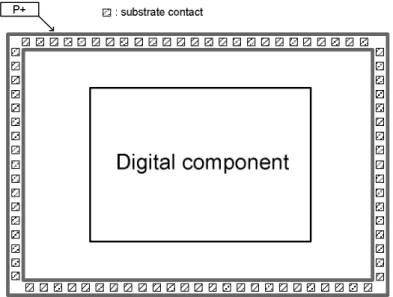
substrate. In digital standard cells, substrate contacts are normally present for latch-up
reasons. Therefore, the number of substrate contacts which illustrated in Fig.2 can be
large in a digital design. Accordingly, the digital ground has formed a very low
Figure 2 Substrate contact of digital ground
Therefore, any voltage fluctuation on the digital ground is also present in the
substrate region of the digital circuit. This noise injection mechanism is normally the
dominant one in digital integrated circuits [1]. If the substrate contacts in the analog
region have a low impedance path to the analog ground, this causes the substrate
noise, in the analog region, to be present on the analog ground. If power supplies of
analog and digital circuit are connected together, a sufficiently high power supply
rejection ratio (PSRR) of the analog circuit is required to prevent lowered
performance degradation.
1.1-2 Capacitive Coupling
receive substrate noise. However, the main contribution to substrate noise normally
originates from the noise injected via substrate contacts [1].There are two types of
coupling ways:The first is capacitive coupling of interconnects;The second is
capacitive coupling of PN-junctions.
C1 C2 C3 Substrate Met al li ne Met al li ne Met al li ne Met al li ne
Figure 3 Capacitive coupling of two adjacent interconnects
In the first place on-chip interconnects are capacitively coupled to the substrate and
adjacent interconnects as illustrated in Fig. 3. The capacitive coupling between the
two interconnects and the substrate is modeled with three capacitors (C1, C2, and C3).
The capacitive coupling of interconnects depends on, e.g. which metal layer
interconnects are located in, the length and the width of interconnects and the distance
to other objects, e.g. interconnects, diffusion area, etc. However, interconnects in the
lower metal layers couple more to the substrate than interconnects in the upper metal
layers. Analog and digital circuits are normally placed in separate regions of the
the case, only when digital and analog circuit use common power voltage line. From
this remarks one general point becomes very clear. The main coupling is through the
substrate.
In the second place, the different doping regions in MOSFETS form parasitic
diodes. For example each PN-junction in an NMOS transistor forms a diode as
illustrated in Fig. 4.
Figure 4 NMOS-transistor with parasitic PN-junction
In CMOS circuit the PN-junctions are usually reverse biased. The parasitic
capacitance of a reversed biased PN-junction is nonlinear and voltage-dependent. This
capacitance can be approximated to
1 2 2 1 1 1 m D bi si A D bi A C V V qε N N V = + −
[2]. A is the area of the PN-junction, V is the built in voltage, and bi V is the D
voltage over the diode. The doping levels for the p region and the n region are
denoted as N andA N , respectively. The gradient coefficient is denoted m, q is the D
the drain and the source of a MOSFET are capacitively coupled to the bulk in CMOS
circuit.
1.1-3 Transmission of substrate noise
Substrates play the role of coupling of noise from one device to another. Over the
past few years a considerable number of studies have been made on substrate model.
Although a large number of studies have been made on substrate model, what seems
to be lacking, however, is the accurate model and parasitic value of resistance and
capacitance for any frequency and manufacture. To understand the occurrence of
substrate coupling, it is important to determine the dominant mechanisms for current
flow in the substrate. Substrate model usually can be constructed with resistance and
capacitance parallel or series connection.
1.1-4 Effect of receiving substrate noise
MOSFETS have four terminals. The drain current is mainly controlled by the gate
source voltage. In analog circuits implemented in CMOS most of the transistors are
NMOS transistor in the saturation region is
(
) (
2)
1 2 n ox D GS tn DS C W I V V V L µ λ = − + (1.1)(
)
0 2 2 th th SB F F V =V +γ V + φ − φ (1.2)In (1.1) and (1.2) it is seen that the drain current is affected by the threshold voltage
(V ), which is dependent of the source body voltage. This effect is known as the body th
effect. Any voltage fluctuation in the body of a circuit can result in a drain current
fluctuation, and further influence NMOS I-V characteristic. Hence, the body effect
which is the conjunction of substrate noise may degrade the performance of analog
circuit.
1.2 Substrate Noise Suppression Technique and
Circuit
Over the past few years a considerable number of studies have been made on
substrate noise suppression. A great deal of effort has been made on substrate noise
reduction method, what seems to be lacking, however, is the ability for wide band
frequency cancellation. Then the purpose here is to explore a little further into
techniques.
1.2-1 Physical methods
A guard ring surrounding the noise receiver or sensitive analog contacts is shown in
Fig.5 [3]. The p+ guard ring is connected to the ground pads using a low-ohmic
contact.
Figure 5 Layout and cross-section of Guard ring surrounding the receiver contact [3]
The ring is a surface-region heavily doped with the majority-carrier doping and is
intended to form a Faraday shield around any sensitive device needs to be protected
compare to other paths for substrate noise in chief and the guard ring steers the
substrate currents to signal ground. Substrate noise in a sensitive circuit can be
reduced if a guard ring is inserted in between a noisy circuit and a noise sensitive
circuit. It is one of the most commonly used isolation schemes and seems to be the
best suited for preventing crosstalk at operating frequencies. In other case of most
modern CMOS technologies use a heavily-doped p+ substrate to diminish latch-up
susceptibility. However, the lower resistivity of the substrate creates unwanted paths
between various devices in the circuit, thereby corrupting sensitive signals. The guard
ring even provides a lower impedance path to ground, but the ratio of heavily-doped
substrate and guard ring is not more than the ratio of lightly-doped substrate. From
this viewpoint one may say that the guard ring maybe not efficiency for substrate
noise suppression, but it is sure to have some isolation ability.
Often theses guard rings are supplemented by placing annular n-type regions
around their peripheries as shown in Fig.6 [5]. The n-well guard diffusion acts to
detach the sensitive analog circuit by interrupting the low resistance channel-stop
Figure 6 Guard-ring supplemented by placing annular n-type regions around peripheries [5].
This way breaks the low resistance path for the substrate noise current by forming a
reverse-biased p-n junction and provides better isolation by forcing the current to flow
through the more resistance p− substrate. In [5], simulation indicate that an n-well
guard diffusion, which breaks the p+ channel stop implant, has almost no effect
because most of the substrate current flows in the heavily doped bulk and not in the
channel-stop diffusion near the die surface. On the other hand, the simulation show
that n-well guard rings are effective when most of the induced substrate current flows
through the p+ field implant region close to the wafer surface of p− substrate.[3]
There are usually good performances by using method of p+ guard ring and n-well
guard ring together for low frequency below 1 GHz. From GHz to far frequency, this
performance decreases rapidly like an exponential decay. Beyond this frequency the
isolation is degraded as frequency increases due to the capacitive nature of the
substrate behavior that kicks in beyond the cutoff frequency.
digital circuits from the back of the wafer. Using an inexpensive mask, a trench can
be etched using potassium hydroxide, KOH, from the backside of the wafer all the
way to the under-surface of the field oxide, resulting in a structure like a trench. [6].
Experiments show that an interference coupling of 35dB above the noise floor is
completely removed when a gap is etched around the analog circuit. The issue of the
approach is the need for and extra mask processing causes extra cost and process
cycle time.
Figure 7 Using KOH to form a trench to protect sensitive circuit [6]
The essentiality of this method must be carefully considered in the design of
SOC because the cost for total processing cost.
Then other papers published the buried substrate shield to go a step further protect
sensitive device. The buried substrate shields can be categorized in three major types.
The first is Faraday shield [7]; the second is dielectric shield [8]; the third is junction
shield [9]. Firstly, a highly conductive layer under the switching devices may provide
a low-impedance path to ground for the substrate noise. However, if used improperly,
[7]. Fig.8 shows layout and cross-section of this way. An experiment done in [7]
shows the effectiveness of this method. Results of the test structure are presented in
Table.1.
Figure 8 Faraday Shield Layouts and Cross-Section [7]
Method With deep contacts Without deep contacts
Without buried layers N /A
248mVpp
Buried layers only under the digital section
105mVpp 183mVpp
Buried layers only under the analog section
75mVpp 232mVpp
Buried layers only under all circuitry
26mVpp 165mVpp
Table 1Comparison of the Different Implementations of Buried Layer [7]
approach physically increases the impedance between the injector and the receiver by
increasing the resistivity of the substrate that surrounds either of the two nodes. This
method is implemented in Silicon-On- Insulator (SOI). In these substrates, bulk
silicon is isolated from the thin active surface silicon layer, by means of buried oxide
layer. The layout and cross-section of this method is shown in Fig.9. This method
provides very good isolation, but it adds to processing costs, since it requires the use
of special silicon substrate [8].
Figure 9 Junction Shield Layouts and Cross-section [8]
between junction shield and dielectric shield is pointed out in Table.2 and showed in
Fig.11 [9].
Figure 10 Junction Shield Layouts and Cross-section [9]
Frequency Dielectric (SOI) Shield Junction Shield
100MHz -66 dB -55dB
200MHz -54 dB -51 dB
400MHz -48 dB -46 dB
700MHz -49 dB -41 dB
1000MHz -48 dB -37 dB
Figure 11 Simulation Result of Comparison between Junction Shield and Dielectric Shield Done by Medici [5]
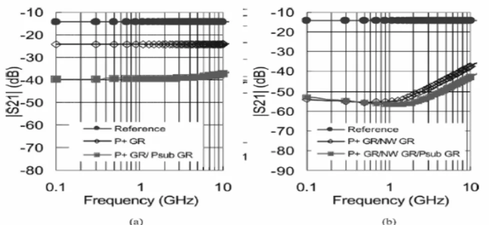
In [10], this paper reports the effect of using a p-minus substrate guard ring (psub
GR) structure to reduce substrate noise coupling. The structure of cross section and
magnitude of S21 versus frequency are showed in Fig.12 and Fig.13. It was found that
integrating the psub GR into conventional GR designs can improve substrate noise
isolation capabilities of conventional p+ guard rings and n-well guard rings by -15dB
and -5dB, respectively.
Figure 12 Cross section of psub GR inserted into (a) p+ guard ring scheme (b) Conventional NW GR with p+ guard ring scheme [10]
Figure 13 Magnitude of S21 versus frequency at an isolation distance of 10um for reference (without any GR) [10]
From results above, although psub GR improve conventional guard ring, it creates
a high resistance surrounding in the receiver port. It will increase latch-up risk in the
real application. The parasitic bipolar transistors and resistors create a parasitic
silicon-controlled rectifier, or SCR. The schematic for the SCR and its behavior are
shown in Fig.14.
Figure 14 Parasitic that cause latch-up
The switching point of the SCR is controlled by the values of the two power
supply resistances R ands R . Because of p-minus increasedw R , the less stray current s
through the tub is required to cause a voltage drop across the parasitic resistance that
tubs and prevents the transistors form operating properly.
Figure 15 Schematic layout of different grounding structure [11]
(a)
Figure 16 The surface potential along the center line through the aggressor ground structure (a) Surface potential illustrating the local and global effects of the ground structure (b) Magnification of the surface potentials inside the ground structure [11]
Two conclusions can be drawn from Fig. 15. First, it is better to distribute the
grounded areas in order to reduce the total ground resistance shown in Fig 16. Second,
the local surface potential is reduced by distributing the ground contacts. It is
represented that its structure provides a similar ideal ground.
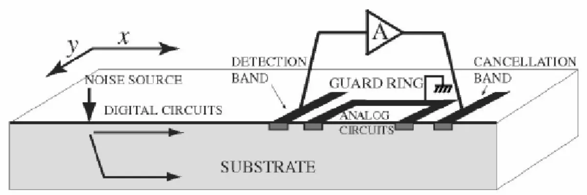
In [12], band connection employed in active cancellation circuits for effective
reduction of digital substrate noise is proposed. Excess cancellation by those band
connections is more effective for noise reduction in a guard ring than a cancellation
by the two bands. The active cancellation circuit shown in Fig. 17 employs an
amplifier with a relatively small finite gain. In order to reduce substrate noise into a
guard ring, noise is detected at a detection band. A cancellation signal is generated by
inverting and amplifying the detected noise. The noise in a guard ring is canceled out
by the cancellation signal. For design of an active cancellation a circuit, a design
guideline that noise at the center of a guard ring is made equal to zero have been
Figure 17 Active cancellation circuit [12]
Using an optimum gain in an active cancellation circuit, a simulation result of a
noise characteristic on a surface of a substrate along the x-axis is illustrated in Fig 18
where the vertical axis shows the noise magnitude normalized with an input noise and
a negative magnitude means an inverted noise is observed. The noise on a guard ring
is zero since a guard ring is grounded.
Because of using inverting and amplifying, the noise is about zero at the center of a
guard ring and fluctuates in the analog area. Thus the noise characteristic in a guard
ring is approximately odd-symmetrical with respect to the center of a guard ring.
Figure 18 Noise characteristic on a substrate surface in the conventional active cancellation circuit. [12]
Fig. 19 shows a layout of bands and band connection and a guard ring and
corresponding noise characteristics. Since a noise between detection band and a guard
ring is positive and that near a cancellation band is negative from the characteristic. A
noise current gathering at the band placed between a detection band and a guard ring
passed to another added band and does little below an analog portion. Thus
propagating into analog circuits becomes smaller.
Figure 19 Noise characteristic when two bands are used [12]
1.2-2 Active circuit noise reduction methods
Passive methods may not be effective enough under noisy situation and may cause
have higher noise suppression level and compensate ability than physical methods.
The resonant forward-biased guard ring diodes for suppression of substrate noise
are proposed in [13], seen in Fig.20.
Figure 20 Model of coupling through substrate in a mixed-mode circuit showing guard-ring diode [13]
The paper has verified that by creating a band-pass filter, using the inductance of
the bond wire and the capacitance of a forward biased diode, the substrate noise can
be reduced [13]. In other words, the resonance creates a very low impedance path to
ground that suppresses the substrate noise. The frequency of the filter is adjusted by
changing the current through the diode and its capacitance. These components form a
band-pass filter, the resonant-frequency of which depends on diode current and is
1
. . / 25
ow
L I
τ
=
Ω
(1.3) Where L is inductance of the bound wire, τ is the transit time and I is diode current.Fig.21 shows substrate noise voltage in two different circuits of with forward-biased
guard-ring and circuit without forward-biased guard-ring.
Figure 21 Effectiveness of Forward-Biased Guard circuit [13]
In [14], this study is based on linear feedback loop theory. Consider a typical
mixed-signal design composed of an analogue portion and a digital portion. The
digital portion of the circuit consists of m different noise sources, and the analogue
portion of the circuit consists of n different noise receivers. Let S denote the noise
source set and N denote the set of noise receivers. At any given time r, the amount of
noise received at the ith noise receiver ri, can be calculated by ( ) 0 ( ) ( )
m
i j j j
r s = Σ = s s ∗H s . If a negative feedback back loop is added to the system as Fig.22 shows and we
assume that the H s are close enough to be replaced by a singlei( ) H s , the noise ri( ) can be expressed as 0
( )
( )
( )
(1
( )
( ))
j m i js s
H s
r s
F s H s
=∗
= Σ
+
(1.4)Where H s is the transfer function of the substrate and ( ) F s is the gain of the ( )
negative feedback loop. The noise to be measured form the noise sensor will be
reduced to 1/(1+F s H s( ) ( )) of the original noise value if a negative feedback loop with sufficient gain-band-width product can be implemented in the system.
Figure 22 Linear system model for analyzing substrate coupling noise with feedback loop [14]
An active guard band filters to suppress substrate coupling noise has been
introduced [15]. An active guard band filter creates a feedback loop using the
seen in Fig. 23. CB1 and CB2 were p+ guard bands or guard rings that were
resistively coupled to the substrate. Capacitor C2 was inserted between GB1 and the
input of the amplifier to detect the AC components of the substrate noise. Capacitor
C1 was inserted between the output of the amplifier and GB2 to supply an AC noise
cancellation signal.
Figure 23 Ac coupling in the on-chip active guard band filter configuration and simplified circuit model [15]
The substrate was represented by resistance R1 and R3. Resistance R2 connected
between the input and output node of the amplifier made the dc operating point stable.
The noise suppression ratio could thus be estimated by using the ratio of Vs to Vi
expressed by
{
1 1 2 2 2}
1 1 1 3 2 3 1 2 3 1 2(1
)(1
)
1
(
)
(
)
s iV
sC R
A sC R
V
s C R
C R
C R
s C C R R
R
A
+
+ +
=
+
+
+
+
+
1 2 1 2
(1
)(1
)(1
)
(1
)(1
)
s
s
A
z
z
s
s
A
p
p
−
−
+
=
−
−
(1.5)Since R1 and R3 were almost equal, the zero and pole frequencies are expressed
as 1 1 1 1 z C R ω = , 2 2 2 1 z A C R ω = + and 1 2 1 1 2 1 ( ) p C C R R R ω =
+ . Since R1 and R3 are smaller than R2, ω is always larger thanz1 ω . However, if A is sufficiently large, the substrate p
noise can be suppressed to 1
A above ω to the amplifier open-loop gain z1
bandwidthω . A
It is found that the conventional AC coupling technique will require large coupling
capacitances which will disable an on-chip implementation of the circuit. In this paper
[16], an active guard band circuit based on a signal cancellation using its opposite
signal is shown in Fig.24. Since the substrate resistances are symmetrical, the transfer
function from node s to nodes g and d will be
2
g d s c s sv
v
v
v
v
v
+
=
=
0
2
s sv
−
v
=
=
Figure 24 Basic of active noise guard band cancellation technique [19]
Figure 25 Active guard band circuit using DC coupling technique [16]
A basic circuit is shown in Fig. 25. Firstly, assume that a noise sourceV , which N
causes voltage fluctuation of substrate level, is detected at node n. Let the drain
current of transistors M and 6 M be2 I .At this time, when the drain current 2
ofM is1 I and1 M , 5 M , 6 M , 7 M have equal aspect ratios, then both drain currents 8
ofM and 3 M will be equal to 4 I and 1 I ,respectively. Thus their gate-source 2
voltages will be equal to VGS1 and VGS2, respectively. Here the relation between
gate-source voltages of transistors M1 and M2 is given by Equ.12 and the relation
between VGS3 and VGS4 can be expressed as Equ.13.
V
X+
V
GS3=
V
B+
V
GS4 (1.7) Because VGS3=VGS1 and VGS4=VGS2.Eq.13 can be written into
V
X+
V
GS1=
V
B+
V
GS2 (1.8) Substituting (1.6) into (1.8) gives
V
X+
V
GS1=
V
B+
V
GS1−
V
N (1.9)V
X=
V
B−
V
N (1.10) and2
2
N X B S DV
V
V
V
=
V
=
=
+
(1.11)Since VB is a constant voltage reference, negative VN will appear at the output node
VX. This means that the substrate noise can be suppressed.
For active method, active decoupling circuit [17] is proposed by using decoupling
capacitor to suppress substrate noise. Its capacitance, C, is multiplied by the gain, A
(w), through the Miller effect. Its active decoupling compared with conventional
capacitor decoupling shows in Fig.26. The decoupling effect in terms of the noise
level with and without decoupling is shown in Fig.27.
Figure 26 Content of on-chip active decoupling and capacitor decoupling [17]
Figure 27 Simulated decoupling effect [17]
In [18], this study demonstrates a feed-forward active substrate noise canceling
technique using a power supply di/dt detector. Since the substrate is tied to the ground
line, the substrate noise is closely related to the ground bounce which is caused by
di/dt when inductance is dominant on the ground line impedance. This active
anti-phase signal into the substrate so that the di/dt proportional substrate noise is
cancelled out. A block diagram of the feed-forward active substrate noise canceling
system is shown in Fig. 28. The ground noise is caused by the power supply di/dt and
Lgnd. Since the substrate noise is proportional to the di/dt, the di/dt detector inverted
output has anti-phase against the substrate noise. If the anti-phase signal is injected
into the substrate, it can cancel the original substrate noise.
Figure 28 Structure of feed-forward active substrate noise cancellation [18]
1.2-3
Summary
Over the past few years, many literatures have been devoted to the study of
well as suppressing substrate noise methods. Here this dissertation focuses on
substrate noise suppression. Many techniques have been investigated to alleviate this
problem for suppressing substrate noise as shown in appendix. Among them, either
passive or active method is used. For the passive method, different guard ring types
are proposed [3], [5-12]. For the active method, feed-back [14], feed-forward [5-19],
[20] and also [17] are proposed.
Among those techniques, passive methods [3], [5-10] may not be effective enough
under noisy situations and may require either special substrate materials or extra
implant/mask processing, which increase cost and process cycle time. In [10], it will
increase latch-up risk in the real application and is not effective in higher frequency.
In [11], these predictive physical researches are valuable reference materials for
circuit designers implementing protection structures for reducing substrate noise.
Other research [12] provides an idea using physical method for enhancing ability of
active guard band circuit and total suppression ability for substrate noise suppression.
Nevertheless such bands located between a guard ring and a cancellation band make a
load impedance of an amplifier in an active band. As a result, a problem of increasing
an output current of the amplifier arises.
On the other hand, although active methods have higher noise suppression level,
and [20], the frequency response and the delay of the amplifier restricts the bandwidth
of the noise being cancelled, so that the noise reduction ratio is not enough for
practical applications and the effective noise suppression bandwidth is only about
100MHz. In [21], although a high noise suppression bandwidth as 400MHz is
achieved by employing a high bandwidth SIGE HBT amplifier, the hetero-junction
bipolar technology is not suitable for the SOC design. In [18], the higher noise
suppression bandwidth as 600MHz is achieved by using power supply di/dt detector,
however, the di/dt device needs mutual inductor to detector. Therefore, this method
needs large area. Finally, in [17] an active decoupling circuit is designed for a wide
operation frequency from 40MHz to 1GHz, but it requires a power-consuming high
gain amplifier and also an area-consuming on-chip capacitor as large as 10-30pF to
obtain a noise suppression level of 6-14dB at most. The summary table of active
methods is shown in Table.3. Because these methods based on different substrate
Reference Technique Bandwidth Isolation Power Area
[21] 0.8um 10M-400M -12 ~ -3dB 13.5mW
[16] 0.6um 1M-100M -13 ~ -11dB >3mW Only MOS
[18] 0.35um 100M-600M -1.6 ~ -3.8dB >3.3mW >238500um2
[17] 0.13um 40M-1G -6dB (max)
-14dB (max)
9.9mW >10000um2
>30000um2
Table 3 Summary table of active methods
1.3 Motivation
In terms of physical level method, its drawback are increasing processing costs
and area and not effective for high frequency. Furthermore existing circuits are
designed for low frequency and does not perform well for wide operation frequency
to reach Giga-Hertz. At present these active circuits require large power and area.
Accordingly, the thesis proposes a new substrate noise suppression circuit with
active guarding technique that employs noise decoupling and inversion feedback to
reduce and suppress the substrate coupling noise. This circuit needs only a few active
devices (PMOS and NMOS), and no capacitors or inductors are needed. Therefore,
with proper design, the area required for this active guarding circuit can be very small,
1.4 Organization
The organization of this thesis is overviewed as follows. Chapter 2 describes active
guarding technique of noise decoupling and inversion feedback and how to design the
noise suppression circuit. The circuit design and optimization will be described in the
same chapter. Chapter 3 shows the implementation and performance results and
measurement. Chapter 4 concludes with a summary of contributions and suggestions
Chapter 2
Active Guarding Circuit Design
and Optimization
2.1 Active Guarding Technique
The proposed active guarding technique is shown in Fig.29. The noise source is
assumed to be a distance away and its current flows through both the surface and the
deep portion of the substrate to the sensitive analog circuit. The active guarding
circuit is in different well from the sensitive analog circuit. In addition, the substrate
model is both resistive and capacitive for high frequency characteristics.
The proposed active guarding circuit composed of noise decoupling and inversion
feedback is inserted by two contact rings between the noise source and the sensitive
analog circuit. These two contact-rings named sense and feedback are applied to
perform noise decoupling and inversion feedback. The noise current flowing through
the sense ring is sensed and averaged then decoupled to the active guarding circuit.
After that, the active guarding circuit re-injects an amplitude-controlled
with the proposed active guarding circuit, only little noise current and only a few
transistors can reach better performance for the guarded analog circuit and the area is
small. Feedback Ring Sense Ring Active Guarding Circuit Noise Source Noise Decoupling Inversion Feedback Guard Ring
Sensitive Analog Circuit Sense Feedback
Figure 29 The proposed active guarding technique
2.1-1 Noise Decoupling
As shown in Fig. 30(a), for the noise current that flows through the substrate to the
sensitive analog circuit, a low impedance path is created for noise decoupling. The
noise current is drained away to the noise decoupling path of the active guarding
circuit. Therefore, the effective noise current that flows toward the sensitive analog
node is Iin, the input impedance of the proposed circuit is Zin_ckt, and the equivalent
impedance of the substrate network at the circuit input node is Zin_sub.
Active Guarding Circuit
Ickt
Iin Isub
Zin_sub
Low impedance path
Zin_ckt Noise decoupling X Ifeedback Inversion feedback Iin Isub Zd Ickt X Y (a) (b)
Active Guarding Circuit
Figure 30 Concepts of active guarding technique (a) Noise decoupling, (b) Inversion feedback
By applying the low impedance path of Zin_ckt on the substrate network, the original
noise current is separated into two parts, Ickt and Isub, which are expressed as
in sub in ckt in sub in ckt
I
Z
Z
Z
I
×
+
=
_ _ _ (2.1)in sub in ckt in ckt in sub
I
Z
Z
Z
I
×
+
=
_ _ _ (2.2)where Ickt presents the current that being drained away by the active guarding circuit
while Isub presents the noise current that flows to the analog circuit. Since the
effective noise current that flows toward the sensitive analog circuit is lowered by a
fraction ofZin ckt_ /(Zin ckt_ +Zin sub_ ) , the noise level at the concerned node X is effectively reduced.
Furthermore, under a given substrate model, Zin sub_ is considered as a known
parameter. Therefore, the only design parameter in equation (2.1) and (2.2) isZin ckt_ ,
the input impedance of the proposed circuit. The smaller the Zin ckt_ is, the more
noise current will be drained away from the substrate and the smaller noise level will
affect the analog circuit to be protected. However, in actual circuit implementation
using MOS transistors Zin ckt_ cannot be arbitrarily small. The smaller Zin ckt_ is, the
larger the MOS transistor size is required, leading higher power consumption. The
design example of proper transistor size will be discussed in later section.
2.1-2 Inversion Feedback
the feedback node rather than to the deep portion of substrate and then to the node X.
The simplified inversion feedback mechanism of the active guarding circuit is
depicted in Fig. 31. M2 M3 VDD
I
ckt Feedback SenseI
cktI
feedback= -I
sub Amplitude ControllerFigure 31 Inversion feedback mechanism
In order to inverse the phase of the noise current sensed from the circuit input, a
current mirror is applied. The phase-inversed noise current is sent to an amplitude
controller to keep the magnitude of the feedback current the same as Isub. Finally, the
magnitude-matched and phase-inversed feedback current is re-injected to the substrate
to cancel the substrate noise current at the feedback node Y.
determined using following equation
( )
( )
sub in ckt in ckt sub C sub C cktZ
Z
I
I
s
A
I
s
A
I
_ _=
=
⇒
=
×
(2.3)However, high frequency inversion feedback performance is limited by the bandwidth
of the current mirror and the amplitude controller. When noise frequencies are higher
than the designed bandwidth, the losses and phase shifts will degrade the noise
suppression performance.
2.2 Circuit Design and Optimization
Fig. 32 shows the schematic of the proposed active guarding circuit. The input
common-gate transistor M1 creates a low impedance path for the sense node and the
impedance value is 1/gm1. Unlike other designs [21] that use the common source
configuration as the input stage to sense the substrate noise voltage from gate, M1 not
only senses the noise current but also drains it away leading to lower noise level for
cancellation in the later stage.
as small as possible. However, smaller 1/gm1, indicates larger transistor size (W/L)1,
which consumes large area and power. To determine the proper size of M1, the noise
suppression improvement per milli-Watt power consumption as the numbers of the
width increment of M1 from 40µm is studied.
M3 M4 VDD
I
ckt Feedback SenseI
cktI
feedback M1 Vbias1 Amplitude Controller Current Mirror Low Input Impedance M5 M7 M6 MR M2 Vbias2Figure 32 Proposed Active Guarding Circuit
Figure.33 shows almost no further improvement of noise suppression is achieved
after the M1 width exceeds 400µm when the noise frequency is 1GHz. The 7th
increment of MOS width, i.e. 320µm is chose as the width of M1, since the
To realize the inversion feedback mechanism, transistor M2~M7 and MR are
added to construct the current mirror and the amplitude controller.
Figure 33 Noise level improved per mW versus M1 width with 40um increment at 1GHz
M4 copies and reverses the phase of the noise currentIckt. The phase-inversed
current is sent to the amplitude controller composed of M5~M7 and MR. The current is
converted to voltage via diode-connected M5 and M6. The transconductance stage M7
adjusts the current gain and converts the voltage back to current to re-inject the
current into the substrate.
To improve the noise suppression at high frequencies, a zero is introduced by
inserting a triode-region transistor MR to extend the effective bandwidth of the active
guarding circuit. Introducing of MR creates a zero and a pole [22] which can be
expressed as 6 5 6
1
,
1
m R m m gdR R gdRg
Z
g
g
RC
P
RC
= −
×
+
= −
(2.4)where R presents the resistance value of MR and CgdR is the parasitic capacitance of
MR.
Moreover, the bandwidth of the active guard circuit can be extended by designing
the zero ZR to be closed to the dominant pole PD of the circuit without MR. The
bandwidth is extended until PR becomes to affect the frequency response. The
dominant pole PD of the circuit without MR can be approximated as
)
||
(
1
P X X DC
C
R
P
≅
−
(2.5) where 5 6 4|| [1 1 ] X o m mR =r g + g , ro4 is the output resistance of M4.
] || ) ( || [ 6 7 7 5 gs sub gd X C C C C C
C = + + , C5 and C6 are the parasitic capacitance of M5 and
4 ( 4|| 3|| 1|| 2)
P gd gs gs gd gd
C =C + C C C C .
2.2-2 Amplitude Controller
Fig. 34 shows the equivalent circuit of the amplitude controller. Transistor M5 and M6
are modeled as resistor 1/gm5, 1/gm6 with their parasitic capacitance C5, C6. MR is
modeled as a resistor R with its gate-drain parasitic capacitance CgdR and
gate-source parasitic capacitanceCgsR. And M7 is a simply transconductance stage.
Feedback
I
cktI
feedback 1/ gm5 1/ gm6 R C5+CgsR C6 CgdRFrom Current Mirror
Z
5Z
6Z
CFigure 34 Equivalent circuit of the amplitude controller
gain A s of the amplitude control circuit can be designed using following C( ) equations
( )
7 5 6 5 feedback C m ckt CI
RZ
A
s
Z
g
I
R
Z
Z
=
=
+
×
+
+
(2.6)For low frequency current gain, i.e. AC(0) can be obtained
( )
7 60
feed ba ck m C ckt mg
I
A
I
g
=
=
(2.7)Refer to equation (2.3) and (2.7), the current gain can be determined as shown in
(2.8).
( )
7 1 6 _1
0
sub m feedback m C ckt in sub ckt mg
g
I
I
A
I
R
I
g
=
=
=
=
(2.8)As a result, for a given Rin sub_ and 1/gm1, the ratio of gm7/gm6 is designed to match
Chapter 3
Implementations and Layout
3.1 Simulation Setup
In order to simulate circuit performance in substrate, a substrate model must to be
established. UMC provided 130nm substrate noise isolation p+ to p+ characterization
and simple structure report and is shown in Fig 35[23]. Therefore, the substrate model
used in the dissertation is built by simulating the model structure shown in Fig 37 (a)
to fit the p+ guard ring characteristic in Fig 36.
Figure 35 Schematics of the reference p+ guard ring, schemes used in the substrate noise characterization [23].
Figure 36 Isolation performance of P+GR schemes vs. frequency for different isolation distance [23].
(a)
(b)
Figure 37 (a) Substrate model structure and (b) Simulation result
compare substrate noise suppression of the circuit (Sample A) and the passive guard
ring (Sample B), and the simulation setup is shown in Fig.38. Therefore, when circuit
is switched on and off, the simulation results can be compared to show the isolation
result provided by active guarding circuit.
Feedback
Sense Out
Passive Guard Ring Active
Guarding Circuit
Sample A
Sample B
Figure 38 Simulation setup of the proposed active guarding circuit
3.2 Measurement Environment
In order to measure active guarding performance, the noise source contact connects
to ESG signal generator and receiver connects to spectrum analyzer. Using one tone
setup.
Figure 39 Measurement setup
3.3 Implementation and simulation results
3.3-1 First implementation
Two implementations were done. The former includes an extra capacitor as shown
discussed in previous chapter. The capacitor would shift the introducing pole to low
frequency location and decrease performance. The circuit layout is shown in Fig 41.
Five different distances from the noise source to the guarding circuit are considered to
measure the substrate suppression capacity in Fig.42. C0 serves as the receive contact
and C1~C5 serve as the noise source inputs. The simulation of DUT1 is shown in Fig
42. The circle symbol (•) of trace indicates isolation of guard ring and the pulse symbol (+) of trace indicates the improved performance of the active guarding ckt compared with guard ring. The measurement results are shown in Fig.43.
Figure 41 Previous circuit layout placement
Figure 43 Previous circuit measurement result data arrangement
From Fig.43, it shows that the measurement and simulation results are not matched.
The mismatch may due to inaccurate substrate model, improper substrate model
resistance and capacitor values, circuit layout or circuit bias. Observe the circuit
layout, a 0.28 um wide VDD line in transistor M7 shown in Fig.44, because 0.28um
VDD line would not tolerate more than 1mA current. Open VDD line is simulated to
verify. The cross symbols of trace indicate the VDD line cut off in Fig.45. Fig.45
show in higher frequency trajectory is similar to measurement data result. But in low
frequency two trajectories of simulation and measurement data are similar. The
mismatch in lower frequency may due to ac couple below 20MHz in the spectrum
analyzer. Therefore, in the second implementation, the spectrum must be adjust dc
suitable VDD line for the second measurementation.
Figure 44 The layout of small VDD line width
Figure 45 Simulation result
Fig.46 shows the noise suppression level of both the passive guard ring and the
active guarding circuit with passive guard ring. The cross symbol of trace indicates
the isolation when the active guarding circuit turned off. And thus other trace
indicates the isolation when it turned on. The result shows that more than 14dB
improvement of noise suppression is achieved by the active guarding circuit
compared with guard ring in the frequency range from DC to 1GHz. The total power
consumption is about 2.86mW
Figure 46 Simulation results of noise suppression versus frequency for both passive guard ring and the active guarding circuit
The circuit layout of active guarding circuit is shown in Fig.47 and circuit layout
area is only 1386 um2. The total layout area is 1.32 mm2 shown in Fig.48. The total
p+ contact. The areas of noise source and receiver p+ contact region are both 7.4 x 13
um2 which is referred to 0.13 um UMC Logic 1P8M Process Substrate NOISE
Isolation P+ to P+ Characterization Report. The isolation distances are varied from
15um to 100um. This placement is referred to the situation similar to 0.13 um UMC
Substrate NOISE Isolation P+ to P+ Characterization Report all the same. This layout
placement is shown in Fig.49 and two different receiver contacts with guard ring and
without guard ring are applied, the comparison of pre- and post-layout simulation is
shown in Fig.50. The plus and cross symbol of traces show the pre- and post- layout
simulation of the active guarding circuit. And the comparison table is shown in
Table.4. Fig 51 shows the noise suppression as the noise level at the sense node
increases from 0.1mV to 100mV at 1GHz. The 1-dB degradation points of the noise
suppression for 1GHz are about 88mV.
Figure 48 Total chip layout
Figure 50 The comparison of pre-simulation and post-simulation
Figure 51 Noise suppression versus input noise level at 1GHz for both passive guard ring and the active guarding circuit.
Technique Bandwidth Isolation Power Area
[21] 0.8um
(SiGe)
10M - 400M -20(max) ~ -3dB
13.5mW
[16] 0.6um DC - 100M -13 ~ -11dB(sim) >3mW Only MOS
[18] 0.35um 100M-600M -1.6~-3.8dB (measurement) >3.3mW 238500um2 [17] 0.13um 40M - 1G -6dB (max)(sim) -14dB (max)(sim) -3.17dB(max) (measurment) 9.9mW >10000um2 (one capacitor) >30000um2 (three capacitor) Proposed work
0.13um DC - 1GHz -15~-14dB(sim) 2.86mW ~ 1386um2 (Only MOS)
Chapter 4
Conclusions and Future Work
4.1 Conclusions
An active guarding circuit for giga-hertz substrate noise suppression has been
implemented in UMC 0.13 CMOS process. With the proposed active guarding circuit,
substrate noise suppression of passive guard ring can be improved more than 14dB in
the frequency range from DC to 1GHz. And Low power and small chip area is
realized with the proposed active guarding circuit for substrate noise suppression. As
a result, this active guarding circuit is suitable for noisy environment with high noise
4.2 Future work
As for the future work, I will focus on the current mirror of active guarding circuit.
As described in chapter 2, the current mirror pole would be settling down higher more
than PR frequency. The pole position will decrease performance for higher frequency
suppression shown in circle symbol of Fig.52. Therefore, high frequency inversion
feedback performance is limited by the bandwidth of the current mirror and the
amplitude controller. This circuit can be improved from current mirror to achieve
better performance in high frequency.
Bibliography
[1] M. van Heijningen, J. Compiet, P. Wambacq, S. Donnay, M.G.E. Engels, and I. Bolsens, “Analysis and experimental verification of digital substrate noise generation for epi-type substrates,” IEEE J. Solid-State Circuits, vol. 35, pp. 1002-1008, 2000
[2] X. Aragones, J. L. Gonzalez, F. Moll and A. Rubio, Analysis and solutions for switching noise coupling in mixed-signal ICs, USA, 1997.
[3] E. Charbon et al.,“Substrate Noise Analysis and Optimization for IC Design,” Kluwer Academic Publishers, 2001.
[4] Behzad, Razavi, Design of Analog CMOS Integrated Circuits International Edition 2001
[5] K. Joardar, “A simple approach to modeling cross-talk in integrated circuits,” IEEE J. Solid-State Circuits, vol. 29, no. 10, pp. 1212-1219, Oct. 1994.
[6] P. Basedau, and Q. Huang, “A post processing method for reducing substrate coupling in mixed-signal integrated circuits,” Symposium on VLSI Circuits ‘95, Digest of Technical Papers, 41, 1995.
[7] X. Aragones, et al., “Analysis and Solution for Switching Noise Coupling in Mixed-Signal ICs,” Kluwer Academic Publishers, 1999.
[8] E. Charbon et al., “Substrate Noise Analysis and Optimization for IC Design,” Kluwer Academic Publishers, 2001.
[9] K. Joardar, “Signal Isolation in BiCMOS Mixed Mode Integrated Circuits,” IEEE Proc. of the Bipolar/BiCMOS Circuits and Technology Meeting, pp.178-181, 1995.
[10] Tsun-Lai Hsu Yu-Chia Chen Hua-Chou Tseng Liang, V. Jan, J.S, “psub guard ring design and modeling for the purpose of substrate noise isolation in the SOC era, ” IEEE Electron device letters, vol. 26, no. 9, 2005
![Figure 6 Guard-ring supplemented by placing annular n-type regions around peripheries [5]](https://thumb-ap.123doks.com/thumbv2/9libinfo/8746314.205061/20.892.134.732.110.291/figure-guard-ring-supplemented-placing-annular-regions-peripheries.webp)
![Figure 7 Using KOH to form a trench to protect sensitive circuit [6]](https://thumb-ap.123doks.com/thumbv2/9libinfo/8746314.205061/21.892.180.712.498.684/figure-using-koh-form-trench-protect-sensitive-circuit.webp)
![Figure 8 Faraday Shield Layouts and Cross-Section [7]](https://thumb-ap.123doks.com/thumbv2/9libinfo/8746314.205061/22.892.244.709.330.729/figure-faraday-shield-layouts-cross-section.webp)
![Figure 10 Junction Shield Layouts and Cross-section [9]](https://thumb-ap.123doks.com/thumbv2/9libinfo/8746314.205061/24.892.228.680.270.717/figure-junction-shield-layouts-cross-section.webp)
![Figure 12 Cross section of psub GR inserted into (a) p+ guard ring scheme (b) Conventional NW GR with p+ guard ring scheme [10]](https://thumb-ap.123doks.com/thumbv2/9libinfo/8746314.205061/25.892.231.627.124.388/figure-cross-section-inserted-scheme-conventional-guard-scheme.webp)
![Figure 15 Schematic layout of different grounding structure [11]](https://thumb-ap.123doks.com/thumbv2/9libinfo/8746314.205061/27.892.237.687.171.480/figure-schematic-layout-different-grounding-structure.webp)