薄膜電晶體主動式矩陣面板之陣列技術研究
181
0
0
全文
(2) 薄膜電晶體主動式矩陣面板之陣列技術研究 Study on Array Technology of Thin-Film Transistor Active Matrix Panel 研 究 生: 陳 紀 文. Student: Chi-Wen Chen. 指導教授: 曾 俊 元 博士 張 鼎 張 博士. Advisor: Dr. Tseung-Yuen Tseng Dr. Ting-Chang Chang. 國 立 交 通 大 學 電子工程學系 電子研究所 博 士 論 文 A Dissertation Submitted to the Institute of Electronics College of Electrical Engineering and Computer Science National Chiao Tung University in Partial Fulfillment of the Requirements for the Degree of Doctor of Philosophy in Electronics Engineering June 2005 Hsinchu, Taiwan, Republic of China. 中 華 民 國. 九 十 四. 年 六. 月.
(3) 推. 薦 函. 事由: 推薦電子研究所博士班研究生陳紀文提出論文,參加國立交 通大學博士論文口試。 說明: 本校電子研究所博士班研究生陳紀文,業已修畢部訂所需課 程學分,通過博士資格考之學科考試,並完成博士論文「薄膜電晶體 主動式矩陣面板之陣列技術研究」初稿,且有數篇相關之論文發表或 送審,茲列舉如下:. International Regular Journals: 1. “Investigation of the electrical properties and reliability of amorphous SiCN”, Thin Solid Film, 447, p.632 (2004) 2. “Study on etching profile of nanoporous silica”, Thin Solid Film, 469-470, p.377 (2004) 3. ” Cu-penetration induced breakdown mechanism for a-SiCN”, Thin Solid Film, 469-470, p.388 (2004). International Letter Journals: 1. “Moisture-induced 2. 3. 4. 5. 6. 7.. material. instability. of. porous. organosilicate. glass”,. Electrochemical and Solid-State Letters, 6(4), F13 (2003). “Effects of Oxygen-Plasma Ashing on Barrier Dielectric SiCN Film” Electrochem. and Solid-State Lett., 8(1), G11 (2005). “Electrical Degradation of N-Channel Poly-Si TFT under AC Stress”, Electrochem. and Solid-State Lett.(accepted) “High Performance Hydrogenated Amorphous Si TFT for AMLCD and AMOLED Applications “IEEE Electron Device Lett. (submitted) “The Influence of Grain Boundary Arrangement on Stability of Poly-silicon TFT” IEEE Electron Device Lett. (submitted) “Low-Temperature Non-volatile Memory Fabricated on Glass Substrate” Applied Phys. Lett. (submitted) “ Temperature Effects of N-channel Poly-Si TFT”, Electrochemical and Solid-State Letters (submitted).
(4) 綜上所陳,陳君已具備國立交通大學電子研究所應有之教育及訓練水 準,謹此推薦陳君參加交通大學電子研究所博士論文口試。. 此致 國立交通大學電子研究所. 電子研究所教授. 曾俊元 博士 張鼎張 博士. 中 華 民 國 九 十 四 年 5. 月. 18 日.
(5) 薄膜電晶體主動式矩陣面板之陣列技術研究 研 究 生: 陳 紀 文. 指導教授: 曾 俊 元 博士 張 鼎 張 博士. 國 立 交 通 大 學. 電子工程學系 電子研究所. 摘要. 本論文首先提出一種具有高導通電流的新穎非晶矽薄膜電晶體元件結構。將 Akiyama所提出之遮光結構(light-shield)結構改善,利用多一次重掺雜的非晶矽 (n+ a-Si)沉積的引入,將縮於閘極內的非晶矽主動區包圍起來,可以有效阻止金 屬與本質非晶矽的接觸,所以光漏電流與暗漏電流皆有明顯改善;此外由於比傳 統BCE 結構多了側壁導通區,使得部份載子可以直接透過側壁進出,有效降低 汲/源極寄生電阻,使得整體新結構非晶矽元件導通能力上升,比相同製程之傳 統BCE結構提升了 50%的導通能力,載子遷移率可達 1.05 cm2/Vsec,新結構元件 可應用於大尺寸電視所需之高導通能力畫素開關元件或是用來驅動有機發光二 極體(OLED)。 此外,由於多晶矽薄膜電晶體能夠整合週邊驅動電路進而由於多晶矽元件 應用於面板週邊驅動邏輯電路時,需要考量到多晶矽元件可靠度的問題,本論文 針對多晶矽元件在AC gate bias stress之後的劣化機制做一深入探討,研究中發現. i.
(6) AC gate bias stress 會造成元件導通電流嚴重的下降,但其起始電壓變化並不 大,根據Seto理論,我們計算出元件劣化前後其有效缺陷密度(effective trap density),由原本的 1.42×1012cm-2增加至 3.14×1012cm-2,並且由其劣化趨勢推論 這些缺陷大部分屬於tail states,同時汲/源極寄生電阻的也急劇增加;藉由在較高 的源極電壓下操作使元件在saturation region (Vds>Vgs)並且有pinch-off region在 汲極附近產生,可以發現導通電流劣化的程度縮小,故可以判定劣化區域是靠近 汲/源極,因為在pinch-off region中,載子不再限定於通道表面傳輸而是可以透過 bulk方式傳輸,若是AC stress產生的大量tail states位於汲極附近的通道表面,當 pinch-off region 在汲極附近產生,載子便可避開這些高電阻區而透過bulk傳輸到 汲極,故其導電特性與會隨汲極端電場而有所變化。 本論文也研究探討多晶矽薄膜電晶體元件的溫度效應,首先對 non-LDD 的 薄膜電晶體做研究,實驗發現 non-LDD 的元件會隨著溫度下降而導通電流增 大,主要原因是因為聲子散射(phonon scattering)的緣故,聲子主要是源由晶格熱 震動所產生,聲子會隨著溫度上升而增加,溫度下降而減少,若載子與聲子間的 碰撞越多其自由路徑會越短,載子遷移率也會隨之下降。然而在 LDD 元件中, 元件導電率與溫度成正比,溫度越高導電率越高,LDD 元件與溫度關係與 non-LDD 元件逕相庭徑,為了釐清兩者之差別,本論文觀察 N+ 與 N- 的片電阻 率隨溫度的關係,然而 N-電阻率隨著溫度上升而嚴重下降,N+ 則較不受溫度變 化影響,由於 N-中摻雜濃度並非達到使多晶矽導電程度達到簡併態,其自由載 子濃度為有效摻雜濃度扣除缺陷態位密度,而隨著溫度下降而參雜活化比率下 降,所以 N-阻值上升,故 LDD 電阻特性對於元件溫度效應中扮演一重要角色, 為確保在適當溫度範圍內面板能正常工作,這些元件的溫度函數是未來電路或是 面板設計上一大考量。 本論文中有探討新型側向結晶方式 Sequential Lateral Solidification (SLS)所 製作出的多晶矽元件其電性與可靠度,由材料分析上可發現 SLS 所產出的晶粒 尺寸比一般傳統 excimer 雷射來得大,我們可以將 SLS 晶界分為二種:一為主晶 界(main-GB),二為次晶界(sub-GB),主晶界的特徵在於其晶界走向垂直元件通 道方向,並且在多晶矽薄膜結構中為一突起(protrusion);次晶界則是平行通道方 向且較平坦,論文中挑選兩種較明顯對比之電晶體進行分析,GB-TFT 為一含有 ii.
(7) 主晶界在通道中央,NBG-TFT 中則僅有次晶界存在,由電晶體參數萃取可發現 NGB-TFT 其起始電壓、次臨界撥動、載子遷移率都比 GB-TFT 優良;然而在 hot carrier stress 實驗中則是 GB-TFT 展現較高的可靠度,透過模擬軟體的計算分析 可發現由於 GB-TFT 通道中央存在有主晶界的存在,這個高缺陷密度的區域能有 效降低汲極端電場,進而降低了 hot carrier effect。 本論文也研究兩種 poly-Si EEPROM 元件結構,一為 floating gate 為儲存電 荷單元,另一為 SiN 為電荷儲存層。本論文首先提出新的 doping 方式來改善 floating gate EEPROM 的閘極電壓耦合效果,可以降低記憶寫入電壓,或是擁有 較快的寫入速度,而且元件導通電流也被提昇了;此外利用 Oxide/Nitride/Oxide 的堆疊,可以在玻璃上製作 EEPROM 元件而達到與晶圓上 MONOS 的記憶效 果,實驗中的穿邃氧化層厚度為 15nm,氮化矽為 15nm,Block oxide 為 25nm, 本論文也發現利用 F-N tunneling 寫入抹除的方式,比較不會破壞多晶矽記憶體 元件的特性,若是以 Channel hot carrier 方式的話會造成元件開關特性的劣化, 起始電壓的飄移,這是由於多晶矽的閘極氧化層為低溫沉積,其品質較晶圓熱氧 化層差,而且熱載子效應會因為玻璃絕緣基板的 floating body effect 而更嚴重, 會使得多晶矽元件閘極氧化層容易劣化。 本論文最後研究具有低 RC 延遲之連線技術,相似於 IC 的多層導體連線技 術發展,Cu 導線與 low-k 材料將是最佳的選擇。本論文先就一種多孔隙的 low-k 材料進行基本特性研究,量測其介電常數並觀察漏電流等等,由於多孔隙材料其 孔隙度高,表面積也相對來得大,容易造成水氣吸附在表面並造成的介電特性改 變。此外,銅金屬與 low-k 材料的整合會面臨到銅金屬擴散造成 low-k 材料劣化, 論文中就水氣造成銅金屬擴散問題作一深入分析,實驗發現水氣會使銅離子更容 易在高電場驅策下而進入 low-k 中。而為了避免銅金屬擴散問題,可以引入介電 阻障層來隔絕銅金屬與 low-k 直接接觸,研究中探討了 SiCN 絕緣薄膜對阻擋銅 擴散的能力的表現,觀察不同氮含量的材料組成對於阻障能力的影響,最後本論 文也提出一個 SiCN 阻障層漏電流劣化的物理模型。 iii.
(8) Study on Array Technology of Thin-Film Transistor Active Matrix Panel. Student: Chi-Wen Chen. Advisor: Dr. Tseung-Yuen Tseng Dr. Ting-Chang Chang. Department of Electronic Engineering and Institute of Electronics College of Electrical Engineering and Computer Science National Chiao Tung University. Abstract. A novel technology for manufacturing high-performance hydrogenated amorphous silicon (a-Si:H) TFT is first developed in this thesis. In the bottom gate light-shield a-Si:H TFT structure, the side edge of a-Si:H island is capped with an extra deposition of heavily phosphorous-doped a-Si layer. Such an ingenuity can effectively eliminate the leakage path between the parasitic contacts between source/drain metal and a-Si:H at the edge of a-Si:H island. In addition, our proposed a-Si:H TFT device exhibits superior effective carrier mobility, as high as 1.05 cm2/Vsec due to the enormous improvement in parasitic resistance. We have evidenced that the leakage current of proposed TFT is lower than the conventional BCE device under bottom-side illumination of 6000 nits. It also exhibits the better ability against the DC current stressing. The impressively high performance provides iv.
(9) the potential of the proposed a-Si:H TFT to apply for AMLCD and AMOLED technology. Next, the temperature and AC gate pulse stress effects on ELA poly-Si TFT have been demonstrated. We find that the conducting current of non-LDD poly-Si TFT is increasing with the decreasing in the temperatures. The phonon scattering is responsible for the evolution of carrier mobility in poly-Si TFT at temperatures. However, the LDD poly-Si TFT is obviously influenced by the LDD layers extended outside the gate electrode. LDD sheet works as a larger resistor at low temperature than that at high temperature. These results can provide the designers to consider the temperature effects for the poly-Si TFT application in a suitable temperature range. In addition, the distinct decrease in ON-current of n-channel poly-Si TFT was found during the dynamic voltage stress. In spite of electrical degradation appearing at the ON-current of the poly-Si TFT, both the sub-threshold swing and threshold voltage kept in a good condition. This can be inferred that the tail states were produced in ploy-Si film due to the AC stress. Additionally, the current crowding effect was increased with the increasing of stress time. The parasitic resistances extracted from the ID-VD curves of poly-Si TFTs were significantly increased after the 1000 s stressing. The effective trap density of poly-Si TFTs stressed for 1000 s was 3.14×1012 cm-2, 2.21 times larger than that of the un-stressed device. The creation of effective trap density in tail-states is responsible for the raise of the parasitic resistance and the degradation in ON-current of TFT. Moreover, the damaged regions whicn contains numerous trap states are evidenced to be mainly located near the source /drain regions. On study the grain –boundary (GB) effects, the comparison of electrical stability between GB and NGB-TFT has been demonstrated. The NGB-TFT owns superior conducting ability than the GB TFT which contains a 100-nm trap-numerous region at v.
(10) the middle of the channel. However, the GB-TFT exhibits the better endurance against DC stress than the NGB-TFT. Based on the simulation result, the existence of GB in the middle of channel of poly-Si TFT would reduce the electric field in the drain region significantly. Accordingly, the GB-TFT suffers relatively lighter impact of hot carrier stress and maintains electrical characteristics well during the DC stressing. The NGB-TFT was seriously degraded by the DC stress with the high electric field at the drain side. Nevertheless, the distinct electrical behaviors of the TFTs were demonstrated under the AC gate bias stress. Due to the existence of protrusion in the channel, GB-TFT shows weaker endurance against the AC gate pulse stress than that of NGB TFT. The magnitude of the vertical field at the protrusion is stronger than the other regions in GB TFT. The strong electric field would lead to the state creation and charge trapping at the protrusion and reduce the device’s electrical performance. On the study of non-volatile memory devices fabricated on glass using low temperature poly-Si technology, two structures have been fabricated and characterized. One is floating-gate device and the other consists of the oxide-nitride-oxide stack structure. The maximum temperature of processing is below 650oC for the glass substrate. The floating-gate memory device consists of two active regions of poly-Si layer, one behaves as the control gate and the other is the conducting channel region. The control-gate transistor of the device is proposed to consist of a whole heavily-doped poly-Si sheet. The higher coupled efficiency of gate bias is demonstrated in the proposed structure. Also, the characterizations of MONOS type memory with an oxide-nitride-oxide (ONO) stack structure were studied. In comparison with channel hot carrier injection, the Fowler-Nordheim tunneling method is more suitable for the programming of the poly-Si memory device. The memory widow of devices can reach 1.5V under the programming voltage of 20V for 10ms.. vi.
(11) The device maintains a wide threshold voltage window of 1.5V after 104 program/erase cycles. Moreover, it retains a good retention property without a significant decline of the memory window up to 50 hours at 60oC. On the study of interconnections with low-RC delay, the porous organosilicate glass (POSG) and a-SiCN have been investigated. The lager leakage current is observed in hot-water dipped POSG sample. The leakage current would be increased and dominated by the ionic conduction as the moisture is contained in the POSG. Additionally, the moisture would enhance the Cu to penetrate into POSG and cause the raise of the leakage current. To avoid the Cu contamination in the interconnections, the electrical properties and stabilities of barrier dielectric a-SiCN films are investigated. The leaky behavior of a-SiCN is evidenced to be Pool-Frenkel conduction in high electric field region. Experimental results indicate that a-SiCN films containing higher nitrogen concentration exhibits better barrier ability. The dielectric breakdown is due to the penetration of Cu. It is observed that the main conduction. of. post-breakdown. a-SiCN. at. room. temperature. (298K). is. space-charge-limited current (SCLC) due to numerous Cu impurity/traps. Moreover, the characteristics at low temperature can be separated into two distinct stages, Fowler–Nordheim tunneling and space-charge-limited current (SCLC) conduction. We propose a physical model which post-breakdown a-SiCN was composed of two different conduction regions. It can well describe the electrical variation resulted from the Cu traps and temperature.. vii.
(12) 誌謝 歷經了數個寒暑,此論文在盛夏蟬鳴聲中逐漸完成,站在求學歷程的回憶長 廊,回頭一望這段眾多人事物交織而成的精彩場景,盡是滿滿的溫暖與感激,是 生命的深刻,深覺意長紙短,實在難以用簡短的文句恰如其分的表現出來。在交 大博士班的修業期間,首先要特別感謝兩位指導教授 — 曾俊元教授及張鼎張教 授,在這兩位教授多年來的教誨與鼓勵下,使我不斷充實成長並得以順利完成論 文。曾教授圓融的處事態度及認真為學的精神,讓學生獲益良多,且於我研究上 遭遇挫折時適時的給予我啟發與鼓勵,是一個博學而仁慈的長者。張鼎張教授費 心指導我論文研究,並於人生規劃上有諸多啟示,而張教授積極處事的態度與研 究創意巧思亦讓學生收穫良多。學生能夠師承兩位師長的指導,我感到十分幸運 與十二分榮幸。 再者,由衷的感謝亦師亦友的劉柏村教授這些年來論文寫作技巧的傳授指 正,並給予我生活處事上的建議,讓學生更能踏穩每一個前進的腳步。另外,也 要謝謝交大半導體中心與國家奈米元件實驗室提供良好的研究設備與環境,還有 工研院電子所提供先進結晶技術的實驗樣品與討論交流,也要感謝友達光電予實 驗上的協助,使論文研究能更加順利與豐富。 一起共同為目標努力的夥伴都是有著難以割捨的革命感情,懷念的不只是一 起奮鬥體會酸甜苦辣的研究生活,還有竹湖夜飲、路邊攤把酒言歡的青春歲月, 非常感謝這些學長、弟妹們︰小莫、小鳴、武群、仁宏、碩廷、鴻明、玟任、阿 娟、蓓欣、政桓、小正、小杰、元均、世仰、子軒、瓊詒、幸儒、皓彥、嘉駿、 國權、震鑠、建良、思漢、崎峰,有你們的幫忙與扶持,讓論文更加順利完成; 另外,也要感謝仍與實驗奮鬥的夥伴們︰永俊、炳宏、致宏、敏全、土撥、國王、 世青、興華、泓緯、志宗、大山及電子所宏澤、家興、昱丞,與其他所有的碩士 班學弟妹,真慶幸有你們陪伴我渡過這充實的博士班歲月,謝謝你們。要感謝的 人實在太多了,還有一些尚未提及的諸多朋友在背後默默的支持我,感謝你們陪. viii.
(13) 我走過這段充實緊湊的日子。 最後,我要感謝全心全意支持我、為我默默付出的父母親,陳章先生與簡麗 珠女士。讓我能無後顧之憂的完成博士班學業,希望我能以此論文的完成讓他們 感受到心靈的安慰與喜悅。 徐徐南風又吹拂過整池的綠荷葉,似乎一抹洗去夏天的煩躁,而我將離開俯 拾皆是回憶的交大校園,此時電資大樓前的荷花也旋即要盛開了吧,這真是令人 珍惜的短促美麗時光,再會了我的朋友。. 僅將此文獻給所有關心我的老師、家人與親友。. 陳. 紀. 文. 誌於 風城交大 2005 年 盛夏. ix.
(14) Contents. Chinese Abstract. ------------------------------------------------------------- i. English Abstract. ------------------------------------------------------------- iv. Contents -----------------------------------------------------------------------x Figure Captions --------------------------------------------------------------xii Chapter 1 Introduction 1.1 General Background 1.2 Thesis Outline. --------------------------------------------------- 1. ----------------------------------------------------------6. Chapter 2 High Performance amorphous Silicon TFT 2.1 Introduction -------------------------------------------------------------11 2.2 Experimental Procedures --------------------------------------------- 12 2.3 Results and Discussions ---------------------------------------------- 13 2.4 Conclusion. --------------------------------------------------------------17. Chapter 3 Investigation of Poly-Silicon Thin Film Transistors with/without LDD Structure at Temperatures and under AC stress 3.1 Introduction -------------------------------------------------------------28 3.2 Temperature Effects on Poly-Si TFTs----------------------------------29 3.3 Electrical Degradation Mechanism of N-Channel Poly-Si TFT under AC Stress ----------------------------------------------------------32 3.4 Conclusion --------------------------------------------------------------- 37. Chapter 4 The Influence of Grain Boundary Location on Low Temperature Poly-Si Thin-Film Transistors 4.1 Introduction -------------------------------------------------------------50 4.2 Device Fabrication. --------------------------------------------- 51. 4.3 Results and Discussions ---------------------------------------------- 52 x.
(15) 4.4 Conclusion --------------------------------------------------------------- 57. Chapter 5 Non-Volatile Memory Devices Fabricated on Glass Substrate Using Low Temperature Poly-Si Technology. 5.1 Introduction -----------------------------------------------------------69 5.2 Device Fabrication------------------------------------------------------71 5.3 Results and Discussions ---------------------------------------------73 5.4 Conclusion--------------------------------------------------------------- 77. Chapter 6 Investigation of the Nano-Porous Interconnections with Low-RC Delay. Silica. for. 6.1 Introduction -----------------------------------------------------------88 6.2 Experimental Procedures --------------------------------------------90 6.3 Results and Discussions -------------------------------------------- 91 6.4 Conclusion-------------------------------------------------------------- -95. Chapter 7 Investigation of the Electrical Properties and Reliability of Amorphous SiCN 7.1 Introduction. ---------------------------------------------106. 7.2 Experimental procedures --------------------------------------------108 7.3 Results and discussions. ---------------------------------------------109. 7.4 Conclusion---------------------------------------------------------------116. Chapter 8 Conclusions and Suggestions for Future Work 8.1. Conclusions-----------------------------------------------------------129. 8.2 Suggestions for Future Work---------------------------135. References -------------------------------------------------------------------------------136 Vita---------------------------------------------------------------------------------------------158 Publication List --------------------------------------------------------------------------159. xi.
(16) Figure Captions Chapter 1 Fig. 1-1. Four structures for a-Si TFTs.. Fig. 1-2. Three possible mechanisms of leakage current in poly-Si TFTs, including thermionic emission, thermionic field emission and pure tunneling.. Fig. 1-3. (a) Plan view of the pixel using low-k passivation technology. dielectric constant (k) material as an inter-level dielectric.. (b) Low. Chapter 2 Fig. 2-1. (a) Conventional inverted-staggered a-Si:H TFT (Structure A). (b) Akiyama’s light-shield a-Si:H TFT (Structure B) (c) The new structure a-Si:H TFT (Structure C). Fig. 2-2. ID-VG transfer characteristics of TFTs, Structures B and C with the same W / L ratio at VD=0.1V. The leakage current of Structure C is effectively suppressed in the proposed TFT structure.. Fig. 2-3. Comparison of ID-VG relations of Structures A and C at VD=10V under the white-light illumination of 6000 nits. The inset sketches the illumination from the bottom-side of the TFTs.. Fig. 2-4. ID-VG transfer characteristics and linear transconductances (gm) of TFTs, Structure A and C with the same W / L ratio. The superior current driving capability of the proposed TFT is demonstrated.. Fig. 2-5. A comparison of output characteristics (ID-VD) for the proposed TFT and Structure C. The current crowding is found in the conventional inverter-staggered TFT, Structure C.. Fig. 2-6. The gate voltage dependence of the parasitic resistance Rp of Structures A and Structure C.. xii.
(17) Fig. 2-7. The distribution of electrons near the drain region in the structures A. The arrow heads labeled in the two figures present the carrier transport directions.. Fig. 2-8. The distribution of electrons near the drain region in the structures C. In the proposed structure, the electrons can transport through contacts, the side wall and the top contact of drain metal overlap region.. Fig. 2-9. The evolution of conducting currents in TFTs during bias temperature stressing (BTS) at 60oC. Initially, both TFTs were conducted with the sam drain current of 200 nA.. Fig. 2-10 The ID-VG relationships of the TFTs after bias temperature stress. The threshold voltage shift of structure A and C is 1.75V and 0.75V, respectively.. Chapter 3 Fig. 3-1. The cross section view of the TFTs in this work. (a)non-LDD TFT (b)LDD TFT. Fig. 3-2. (a)The ID-VG relations and transconductance, gm, of poly-Si TFT at the temperatures from 50K to 250K. (b) drain current in linear scale.. Fig. 3-3. Three types of scatterings in MOSFET devices, including impurity scattering, surface scattering and the phonon scattering.. Fig. 3-4. The ID-VG relations of LDD-TFT at the temperatures from 50K to 300K.. Fig. 3-5. The sheet resistances of phosphorous (a)heavily-doped and (b)light-doped poly-Si film at the temperatures from 50K to 300K.. Fig. 3-6. The LDD layers extended out the gate overlap region behave as the temperature-dependent resistors and series connecting with the gate control region. xiii.
(18) Fig. 3-7. The stress pulses were conducted on the gate electrode as the dynamic stress and source/drain were grounded. The rectangular pulse with amplifier of ±15V and frequency of 500kHz. Both the rising time (Tr) and falling time (Tf) were 100 ns.. Fig. 3-8. The ID-VG relationships of n-channel poly-Si TFT (L=9μm) with the dynamic stress times for 10 to 1000 seconds.. Fig. 3-9. The ID-VD characteristics of the TFT with the dynamic stress times.. Fig. 3-10 The gate voltage dependence of the parasitic resistance Rp of TFT with various stressing times. There is a distinct raise in Rp of poly-Si TFT after 1000 s. Fig. 3-11 (a), (b), and (c) present the effective trap density (Nt) of poly-Si TFT with AC stress for 0, 100, and 1000 s, respectively. The Nt of the device with 1000 s stress is 2.21 times larger than that of the non-stressed poly-Si TFT. Fig. 3-12 ID-VG curves of poly-Si TFT at saturation operation (VD=8V) with AC stress for 0 to 1000 s. The degradation in ON-current with the high drain bias is much weaker compared to the linear ones. The inset figure indicates that carriers can spread to the bulk at the pinch-off region near the drain electrode.. Chapter 4 Fig. 4-1. (a) The top view of a high-resolution scanning electron microscopy (SEM) image of SLS laser annealed poly-Si film. The orientation of main-GB and sub-GB is perpendicular and parallel to channel direction of the TFTs we utilized, respectively. (b) The AFM image of SLS poly-Si film, the height of protrusion is about 100nm at the grain boundary region.. Fig. 4-2. (a) GB-TFT owns a main-GB in the middle of the channel. NGB-TFT lies in the main-GB free region. (b) The microscope picture of GB TFT (c) The microscope picture of NGB TFT. xiv.
(19) Fig. 4-3. ID - VG transfer characteristics of NGB and GB TFTs with the same W / L ratio. The NGB TFT has larger field mobility (283.2 cm2/Vsec) than that of the GB device (262.5 cm2/Vsec)... Fig. 4-4. The capacitance-voltage (C-V) characteristics of GB and NGB TFTs. The CV transition curve of GB TFT shows a slightly slow in comparison with the NGB TFT.. Fig. 4-5. ID - VG relations of NGB-TFT in linear and logarithm with the stress for 0, 10, and 100 s. After stressing for 100 s, the on-current of TFT at VG=20 is degraded to 12% of the magnitude of the initial value.. Fig. 4-6. ID - VG relations of GB-TFT in linear and logarithm with the stress for 0, 10, and 100 s.. Fig. 4-7. The electric distribution in the channel region of the TFTs under the bias conditions VG=6V and VD=12V. The main-grain locates at the center of the channel in GB-TFT. For GB-TFT, the maximum of electric field at the drain shows about 27% lower than that without grain boundary in the channel.. Fig. 4-8. The ID-VG relations of NGB TFT with the dynamic stress times for 10 to 1000 s. The mobility of NGB TFT is decayed from 282.9 to 204 cm2/Vsec after 1000s stress.. Fig. 4-9. The ID-VG relations of GB TFT with the dynamic stress times for 10 to 1000 s. The mobility of GB TFT is decayed from 243 to 136.9 cm2/Vsec after 1000s stress.. Fig. 4-10 The distribution of electrical field at (a) the protrusion and (b) smooth plane.. Chapter 5 Fig. 5-1. (a) The planar view of the poly-Si TFT EEPROM which is composed of two active regions, T1 and T2, of poly-Si layer. (b) The cross section of the xv.
(20) device A (c) The cross section of the device B. The T2 region of device B, control gate, is wholly doped with heavy dose of boron. Fig. 5-2. (a) The scheme of MONOS (Metal/Oxide/Nitride/Oxide/Poly-Si) type flash memory. (b) The Transmission Electron Microscope (TEM) cross-section of ONO on the poly-Si surface.. Fig. 5-3. (a) The comparison of ID-VG relations at VD=0.1 between the memory devices, A and B. (b) The ID-VG relations of the memory device A and B after electrical programming with the gate bias of 18V and erasing with 22V for 10ms.. Fig. 5-4. The effects of the gate voltage on the programming and erasing characteristics of poly-Si TFT EEPROM’s. The magnitude of voltage shift tends to be saturate with the raising of the programming time.. Fig. 5-5. The endurance characteristics, after different program/erase (P/E) cycles, of the device B. The P/E of the memory devices was performed by applying negative (18V) and positive (-22V) voltage pulses, respectively.. Fig. 5-6. The threshold-voltage shift is measured with different periods of time when the sample is heated at 60oC.. Fig. 5-7. The ID-VG relations of the poly-Si MONOS memory device after electrical programming with the gate bias of 20V for 10 ms.. Fig. 5-8. The ID-VG relations and linear transconductance gm of the device were after programming using CHE method with the drain bias of 35V and 45V at VG=25V, respectively.. Fig. 5-9. The endurance characteristics, after different program/erase cycles, of the MONOS memory device. The program/erase (P/E) of the memory devices can be achieved by applying positive (+20V) and negative (-40V) voltage pulses, respectively.. Fig. 5-10 The threshold-voltage shift is measured with different periods of time when the sample is heated at 60℃.. xvi.
(21) Chapter 6 Fig 6-1. The FTIR spectra variation of as-spun porous organosilicate glass (POSG) after undergoing a series of thermal process.. Fig 6-2. Three-dimensional (3D) network structure of POSG.. Fig 6-3. The evolution of stress of POSG with the hot-water dipping for 1 to 3 hours.. Fig 6-4. The thickness variation of POSG with the hot-water dipping for 1 to 3 hours.. Fig 6-5. The FTIR variation of POSG with the hot-water dipping for 1 to 3 hours.. Fig 6-6. The leakage currents of POSG increase with the increase of hot water dipping time, whereas the leakage currents decrease obviously after water-dipped POSG film (for 3 hr) undergoes 300℃ furnace annealing.. Fig 6-7. The J-E relations of POSG samples at room temperature. The moisture-containing sample owns the larger leakage current that the standard sample which is moisture-free at the same bias.. Fig 6-8. The thermal desorption spectra of moisture-containing and STD samples. The magnitude of H2O signal (m/e=18) in moisture-containing sample is larger than that of STD sample.. Fig 6-9. (a) The leakage current v.s. time (I-t) characteristics of Cu and Al-electrodes POSG during the bias stress at room temperature and 150oC, respectively. (b) The J-E curves of Cu and Al-electrodes POSG before and after the RT stress.. Fig 6-10. (a) The SIMS spectrum of POSG with Al-electrode after RT stress. (a) The SIMS spectrum of POSG with Cu-electrode after RT stress.. xvii.
(22) Chapter 1. Introduction. 1.1 General Background Thin film transistor (TFT) is a metal-oxide-silicon field effect transistor (MOSFET) fabricated on an insulator substrate by employing all thin film constituents. Thin film transistors have been widely used as switching devices in flat panel display, such as active-matrix liquid crystal display (AMLCD)[1.1-1.5] and active-matrix organic light emitting diode (AMOLED) display. [1.6-1.10] The thin film transistors can be mainly divided into two types according to the active layers, amorphous and poly-crystalline ones. The amorphous TFT is usually applied in large size flat panel display due to its mature manufacture and low-cost. On the contrary, poly-Si TFT is suitable for the high-resolution medium and small size flat panel display. The high mobility of a-Si TFT is required for high resolution AMLCD since the charging time of pixel is shorter than the low resolution one. However, the numerous trap states existed in a-Si layer seriously strict the transporting of carriers.[1.11-1.13] The application of poly-Si TFT is attractive due to the higher mobility than the a-Si one. The higher mobility and existence of complementary devices lead to integrate functional circuits on the display. Moreover, introduction of the new device, such as EERPOM, can increase the feasibility of circuit design for the flat panel.[1.14-1.15] The improvement of electrical characteristics and understanding of degraded mechanism of TFTs is important for development of display technology. Additionally, the interconnections with low-RC delay have been received increasing attraction in the ICs and flat panel display applications. To improve the. 1.
(23) performance of ICs, the scaling down for integrated circuits is necessary. The shrinkage in critical dimension of active devices would also result in smaller linewidth and spacing between metal interconnections. Moreover, the length of interconnection lines will increase due to the larger chip size, which is the result of getting profitable and excellent IC performances. As a result, a larger part of the total circuit propagation delay (RC delay) is contributed more from the characteristics of the interconnections than that of the scaling of devices. [1.16-1.20] Similar to the RC delay issues in ICs fields, the lager-area flat panel display such as active matrix liquid crystal displays (AMLCD’s) are also currently suffered the RC delay impacts.[1.21-1.22] Large-area high-resolution AMLCD are on their way to becoming an elegant alternative to CRT displays in televisions. However, several fundamental scaling problems are encountered when trying to increase the display size. One of them is associated with the gate metallization for the inverted-geometry thin-film transistors (TFT’s) of the active matrix. At present, refractory metals such as tantalum/ molybdenum are used, to ensure stable contacts during TFT fabrication. The gate lines are deposited first onto the glass backplane. They must be thin to ensure good step coverage by the plasma-enhanced chemical-vapor deposited (PECVD) layers. The relatively high refractory metal resistivities result in RC gate delays that restrict the AMLCD size. It is obvious that the gate line pulse suffers distortion as it moves through the line. The distortion increases the rise time and delays the arrival of the gate pulse. The delay can cause the gate and data pulses to arrive at a pixel out of synchronization. As a result, low resistivity metals and low-dielectric are required for high-performance ICs and large-area AMLCD’s.. 1.1.2. Thin film transistors technology. 2.
(24) Amorphous silicon technology is quire attractive due to its low processing temperature and low cost manufacture. The hydrogenated amorphous silicon (a-Si:H) thin film transistors (TFT) have been applied on the flat panel displays and X-ray sensor arrays. There are four structures for a-Si:H TFT’s, including staggered, inverted staggered, coplanar and inverted coplanar TFT’s, as shown in Fig 1-1. Among these four structures, the inverted staggered one is most popular due to its simple. process. and. acceptable. electrical. characteristics.. Therefore,. the. inverted-staggered back-channel-etched (BCE) type of a-Si:H TFT has been widely used as a switching element to control the gray level in liquid crystal display(LCD) and to drive organic light-emitting-diode (OLED). With increasing the resolution and size of AMLCD, the charging time of the pixel is decreased with a fixed frame rate. Except to reduce the RC delay of interconnections, the a-Si TFT with high driving capability is required for the large area AMLCD. In addition, a-Si:H TFT with high stability and driving capability is suitable for AMOLED application since OLEDs require a current driving scheme in contrast to LCD, which are voltage driven. Compared with a-Si TFT technology, the poly-Si TFT technology has some distinct advantages but its manufacture is more complex and high cost. The major advantage of poly-Si TFT is the higher field effective mobility than that of the amorphous silicon (a-Si) based devices. The high carrier mobility and the existence of complementary pairs permit the integration of drive circuits and the smaller area of pixel transistor. The integration of drive circuits could reduce manufacturing costs, and increase the functionality of large-area microelectronics.[1.23-1.24] The smaller area of pixel transistor leads to a larger aperture ratio for a given pixel size, or enables a higher resolution display for a given aperture ratio, resulting in better image quality. Moreover, the poly-Si TFT could be applied to the active matrix organic light emitting. 3.
(25) diode (AM-OLED) display due to its high current driving capability. The degree of circuit integration will continue to increase as device characteristics improve further. Additionally, the new functional devices fabricated on the glass can increase the flexibility of circuits for the display. The nonvolatile memories, such as flash memories and electrically erasable PROM’s (EEPROM’s) fabricated on the wafer, have been widely used for the applications of high-density memories, programmable logics, and microcontrollers. [1.25-1.26] Similarly, the applications of non-volatile memories on the system of flat-panel are attractive. The smart cards consist of memory and RF logic circuits can be fabricated on the low-cost substrate such as plastic and glass ones. In poly-Si TFT devices, however, the status of defect states at grain boundaries plays a crucial role for electrical characteristics, as shown in Fig. 1-2. The stability of poly-Si TFT is one of the important issues for poly-Si technology. Recently, there have been several investigations about the stabilities of poly-Si TFT’s. The creation of trap states at poly-Si/gate dielectric interface or the charge trapping in the gate insulator is responsible for the degradation in electrical characteristics of poly-Si TFTs. Since the large area electronics or the flat-panel displays comprised of poly-Si TFTs are used by peoples at the globe, the displays should keep the performances well at temperatures. However, temperature usually influences the characteristics of solid-devices, and relative effects are important for the application of Poly-Si TFT technology. Consequently, it is important to introduce the new functional device into poly-Si technology and understand the fundamental properties of poly-Si TFTs such as electrical stressing degradation, grain boundary effects, and temperature effects.. 1.1.2 Interconnections with low-RC delay 4.
(26) The RC delay of interconnections is mainly contributed to the resistivity of metals and capacitors of insulators. In the medium 1990’s, the National Technology Roadmap for Semiconductors (NTRS) described the first needs for new conductor and dielectric materials to meet the projected overall IC technology requirements [1. 27]. Similarly, some of research reports have shown that the gate pulse delay is getting serious with the increasing of the size of large area AMLCD. The resistance and capacitance (RC) delay of the gate line retards the turnoff of the transistor at the far end of the gate line.. Moreover, the coupling capacitance resulting from pixel. electrode and the data and gate line would lead to the cross-talk and signal distortion. To minimize the coupling capacitance, the low-k materials should be introduced into the interconnection of flat panel display. Also, the implantation of low-k in display can achieve a high aperture ratio for improved light transmittance or image quality, as shown in Figs. 1-3(a) and (b). This requires a thick, low dielectric constant (k) material as an inter-level dielectric. Thereafter, there were many new interconnect materials and structures extensively studied in the industrial and academic committees. For the low-resistivity materials, Cu conductive metal has been recognized to apply to IC technology and flat panel displays due to its low resistivity (1.67 μΩ-cm for bulk materials) and high electromigration resistance. [1.28-1.29] Moreover, the investigation of low-k materials on its physical, chemical and electrical properties is very important for the progress of display technology. There are two principal methods to form low-k films. One is the chemical vapor deposition (CVD), and the other is the Spin-on deposition (SOD). The conventional passivation material was CVD deposited nitride whose dielectric constant is about 6~7. Moreover, CVD method is easily compatible to the standard display processes. The other technique of forming low-k materials is spin-on deposition (SOD). This 5.
(27) method is using a liquid precursor deposited by spin-coating or spray method. Then, the substrate is subjected to a series of baking. Finally, a furnace curing or UV curing s performed to achieve the network low-k structure. Some SOD low-k materials, additionally, can be patterned by photolithography. The SOD type of low-k materials possesses the features of good gap filling, local planarization and low dielectric constant. In general, most of SOD low-k materials can be divided into two categories. One is organic polymer, and the other one is inorganic silica-based materials. The interconnections made of Cu and low-k owns lower RC delay to meet the requirements in advance IC and display application. However, one of the reliability issues in Cu/low-k metallization is the dielectric degradation caused by Cu ion penetration. Copper rapidly drifts in silica-based low-dielectric-constant (low-k) materials during bias-temperature stressing (BTS). Moreover, the Cu atom plays as the generation/combination trap center in Si films and seriously influences the performance of Si-based devices. The insertion of barrier dielectrics between Cu wiring and low-k dielectrics is essential for a reliable copper interconnect technology. Silicon nitride (SiNx) is a good barrier dielectric and efficiently prevents the Cu drift,3 but its dielectric constant is too large (~7). SiNx, thereby, needs to be substituted to reduce the effective capacitance for interconnection applications.4 Studies on barrier dielectrics with lower dielectric constants related to SiNx, are receiving much attention. Recently, silicon-carbie (SiC) based materials with k<5 are proposed for the barrier dielectric applications.5-6 But the reliability and degraded mechanism have not been investigated detail.. 1.2. Thesis Outline. The dissertation is organized into the following chapters: In chapter 1, a brief overview of the TFT technology and the interconnections with 6.
(28) low-RC delay is introduced to describe the various applications of them. We describe the trend of TFT technology development and the degradation of low-k caused by Cu penetration. Then, the outline throughout the dissertation is discussed here. In chapter 2, a new structure of beck-channel etching (BCE) a-Si TFTs was first proposed. This novel device owns superior performance than the conventional one. The ON-current of the new devices is 1.5 times the conventional BCE device. Moreover, the proposed device owns low leakage current either in dark or under bottom-side illumination. In chapter 3, the temperature and AC stress effects on poly-Si TFT are studied, separately. The electrical characteristics of n-TFT with/without LDD are measured at temperatures. The characterizations of the n-TFTs without LDD under AC gate-bias stressing are investigated to clarify the degradation mechanism. Chapter 4 contains two parts. For part I, the grain boundary effects of poly-Si TFT were discussed. The electrical properties of TFTs are compared to clear the carrier transport in poly-Si TFT . For part II, the influence of grain boundary in reliability is investigated under DC and AC stress. In chapter 5, we demonstrated two kinds of the non-volatile memory devices fabricated using low-temperature poly-Si technology. The programming and erasing methods for poly-Si memory devices are also investigated. Moreover, the electrical characteristics and reliabilities of devices In chapter 6, the intrinsic properties of low-k nano-porous silica and the impact of moisture absorption for interconnect applications are investigated. In addition, the reliability of nano-porous silica with Cu electrode using bias-stressing method is also demonstrated in this chapter. In chapter 7, the intrinsic properties of barrier dielectric film, a-SiCN, are investigated. The breakdown mechanism of barrier dielectric caused by Cu penetration is depicted. 7.
(29) In chapter 8, we summarize our experimental results and give a brief conclusion. Recommendations of several topics relevant to the thesis are also given for further study.. Fig. 1-1 Four structures for a-Si TFTs.. 8.
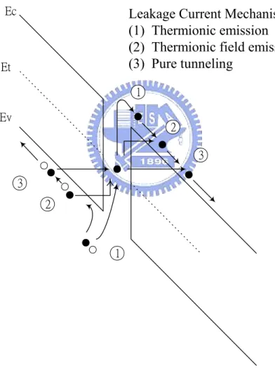
(30) Ec. Leakage Current Mechanism (1) Thermionic emission (2) Thermionic field emission (3) Pure tunneling. Et. 1 Ev. 2 3 3 2. 1. Fig. 1-2 Three possible mechanisms of leakage current in poly-Si TFTs, including thermionic emission, thermionic field emission and pure tunneling. 9.
(31) Fig. 1-3 (a) Plan view of the pixel using low-k passivation technology. (b) Low dielectric constant (k) material as an inter-level dielectric. 10.
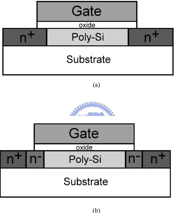
(32) Chapter 2. High Performance amorphous Silicon TFT 2.1 Introduction. Amorphous silicon technology is very attractive due to its low processing temperature and low cost manufacture. The hydrogenated amorphous silicon (a-Si:H) thin film transistors (TFT) have been applied on the flat panel displays and X-ray sensor arrays. There are four structures for a-Si:H TFT’s, including staggered, inverted staggered, coplanar and inverted coplanar TFT’s. Among these four structures, the inverted staggered one is most popular due to its simple process and acceptable. electrical. characteristics.. Therefore,. the. inverted-staggered. back-channel-etched (BCE) type of a-Si:H TFT has been widely used as a switching element to control the gray level in liquid crystal display(LCD) [2.1-2.5] and to drive organic light-emitting-diode (OLED). [2.6-2.12] TFT with a large switch ratio and low off-state leakage current is suitable to control LCDs. In addition, a-Si:H TFT with high stability and driving capability is suitable for AMOLED application since OLEDs require a current driving scheme in contrast to LCDs, which are voltage driven. The a-Si:H material is a well-known photoconductor and its conductivity increases drastically resulting from the generation of electron-hole pairs under illumination of a visible light.[2.13-2.15] However, LCD panels are usually used in an illumination environment such as under the back-light. Therefore, the leakage current of TFT under back-light illumination in TFT-LCD displays should be reduced to avoid losing the storage charges in the pixel. Akiyama et al. has demonstrated the light-shield 11.
(33) structure for the TFT using in AMLCDs.[2.16] Figure 2-1(a) and 2-1(b) show the conventional and Akiyama’s structures, respectively. The major difference between them is that a-Si:H island is completely located inside the coverage of gate metal in Akiyama’s structure. The gate metal effectively shields the back-light irradiating to a-Si:H layer, as shown in Fig. 2-1(b). However, the edges of a-Si:H island are direct contact with the source/drain (S/D) electrode, when the TFT fabricated with the deposition of metal deposit on the tri-layer(SiNx/ a-Si:H/n+ layer), as shown in Fig. 2-1(b). The metal/a-Si:H contact usually exhibits the Schottky type conduction, being subjected to the leakage.[2.13] We propose a new and convenient technology to reduce the leakage current originated from the leaky contact between the metal and a-Si:H layer in this study. The turn-on current of the proposed TFT is also increased due to the reduction in parasitic source/drain resistance. Moreover, the proposed TFT exhibits better stability than the conventional BCE TFT under the current stress.. 2.2 Experimental Procedure. The fabrication process of the proposed TFT device is described as below. The inverted staggered a-Si:H TFT’s were fabricated, but the a-Si:H active island of TFT is located inside the coverage of gate metal electrode. First, metallic Cr was deposited on glass substrates by sputtering and then was patterned to form gate electrodes. It was followed by SiN, undoped a-Si:H and phosphorous-doped a-Si:H (n+ a-Si:H) layer deposition sequentially on the Cr patterned glass, without breaking the vacuum in a plasma-enhanced chemical vapor deposition (PECVD) chamber. The SiN layer was deposited using a mixture of SiH4 and NH3 gases at a substrate temperature of 300oC and the undoped a-Si:H was deposited from a gas mixture of H2 and SiH4 at 12.
(34) 300 oC. The film thickness of Cr, SiNx, a-Si:H and n+ a-Si:H layers was 150, 200, 150 and 20 nm, respectively. The definition of a-Si:H active region was performed with lithography and etching processes. In our proposed new TFT, the second layer of 20-nm-thick n+ a-Si:H film was deposited to clad the active regions. Aluminum film was evaporated to form the source/drain electrodes. Finally, the patterned Al films were used as a mask to etch back the channel to isolate the source and drain electrodes of TFT. In the proposed process, only three masks were required to fabricate TFT and the number of mask is equal to the conventional BCE procedure. Figure 2-1(c) illustrates the new structure of our proposed light-shied TFT device. It should be noted that the proposed TFT described above consists of 20nm n+ layer at the edge and 40nm n+ layer on the top of the active island. We performed the DC stress using Agilent 4156 analyzer on the TFTs to evaluate the stability of TFTs.. 2.3Results and Discussions. The solid and dashed lines in Fig2-2 indicate transfer characteristics of light-shield a-Si:H TFTs fabricated with conventional as well as our proposed process, respectively. The leakage current of Akiyama’s light-shield TFT is as high as two order the proposed TFT under the simialr negative gate voltages. The S/D metal/intrinsic a-Si:H contact at the edge of a-Si:H island, as shown in Fig. 2-1(b), usually behaves as the Schottky emission.[2.13] On the contrary, the capped n+ a-Si layer on the a-Si:H island effectively avoids the direct contact between a-Si:H and S/D metal, as shown in Fig. 2-1(c). The n+ a-Si:H layer can effectively block the hole current when the gate is biased with negative voltages. The leaky path between the metal/intrinsic a-Si:H was thus eliminated and the leakage current was reduced. Under. 13.
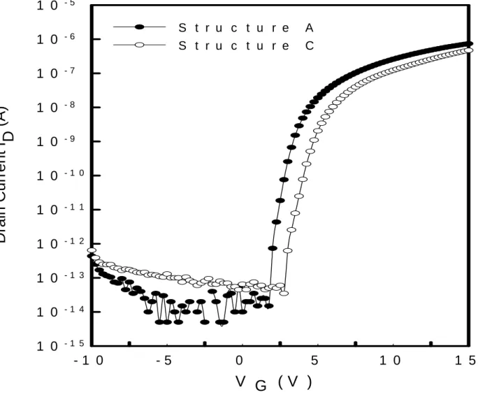
(35) the same applied gate voltages, the leakage current of Structure C is two orders of magnitude lower compared to the Structure B. In addition, the proposed TFT structure exhibits superior current driving capability, as shown in Fig. 2-3. The turn-on current of the new TFT is about 1.5 times higher than that of Structure A, the conventional inverter-staggered counterpart. Using the proposed structure in this work, the TFT with effective mobility of 1.05 cm2/Vsec extracted at Vd = 0.1V was obtained. The carrier mobility of conventional inverter-staggered TFT, structure A, fabricated with the same process is 0.72 cm2/Vsec. Moreover, the threshold voltage of the proposed TFT is 2.3V, extracted at current density of 1 nA with normalized channel width (W)/channel length (L) ratio and lower than the conventional inverter-staggered one (2.8V). To compare the leakage current between the proposed and the conventional BCE TFTs under illumination, the electrical measurements were performed under white-light illumination of 6000 nits underneath, as sketched in the inset of Fig. 2-4. Fig. 2-4 illustrates that the proposed structure has lower leakage current than that of the conventional BCE Structure A device at Vd=10V under the illumination of 6000 nits. Meanwhile, the devices were operated with drain bias of 10V at saturation region (VD>Vgs-VT) since the photo-induced leakage current would be enhanced by the high drain bias. The electrical characteristic of the inverter-staggered a-Si:H TFT suffers from the parasitic resistance.[2.17-2.18] The parasitic resistance is dependent on several factors, for instance, the thickness of a-Si:H, sheet resistance of n+ a-Si layer, and source/drain contact quality. For a constant W/L ratio, the effect of parasitic resistance can be clearly observed in the output characteristics of a-Si:H TFTs. The large parasitic resistance would result in the current crowding effect. A comparison of output characteristics (ID-VD) for the new TFT and the conventional TFTs under nominal W/L ratio is shown in Fig. 2-5. The current crowding is found in the 14.
(36) conventional inverter-staggered TFT, not observed in the proposed TFT device. The significant difference in device structure is an n+ a-Si contact formed at the sidewall of a-Si:H island (a-Si:H/n+a-Si) in the proposed TFT, as shown in Fig. 2-1(c). To investigate the difference of electrical characteristics between Structures A and C, the parasitic resistances of TFT devices were extracted. Under the operation of small drain voltages VD and high gate voltages VG, it is assumed that the turn-on resistance Ron of TFT device consists of the channel resistance Rch and the parasitic source/drain resistance Rp. Ron = Rch+Rp , and Rch =. L WμC i (VG − VT ). where Ci is the gate nitride capacitance per unit area and W, L, and Vt are the intrinsic device channel width, length, and the threshold voltage, respectively.[2.17] The parasitic resistance RP of a-Si:H TFT can be extracted through measuring the ON resistance Ron from the linear region of TFT output characteristics and through plotting the RonW against the channel length L.[2.17-2.20] Figure 2-6 illustrates the typical gate voltage dependence of the parasitic resistance Rp of Structures A and Structure C, comparatively. The Rp value of the proposed TFT is significantly lower than that of the conventional one. Moreover, the Rp of the conventional inverter-staggered TFT is strongly dependent on the gate voltages. The value of Rp decreases from 6.6 MΩ to 2.2 MΩ, when the gate voltage increases from 6V to 12V. By contrast, the gate-voltage dependence of the Rp of the proposed TFT is weaker and just decreases from 1.2 MΩ to 0.5 MΩ. In the proposed TFT device, the lack of an intrinsic a-Si:H layer between channel and source/drain contacts can reduce such nonlinear. effects,. as. similar. to. the. space. charge-limited. conduction. (SCLC).[2.19-2.20] The SCLC occurred in intrinsic a-Si:H region is influenced seriously by both the drain and gate voltages. Also, the simulation results indicate that. 15.
(37) the carriers can be transported form the channel to the n+ layer at the sidewall of a-Si:H island and are quite different from those having an intrinsic layer between n+ a-Si layer and the channel. Figures 2-7 and 2-8 illustrate the distributions of electrons near the drain region in the corresponding structures A and C. The arrow heads labeled in the two figures present the carrier transport directions. In the proposed structure, the electrons can transport though contacts, the side wall and the top contact of drain metal overlap region. By the contrary, the conventional inverted staggered TFT owns one path for transporting, from the bottom accumulation layer of the a-Si:H layer to the top contact of metal. Hence, the lower parasitic resistance of the proposed TFT results in relatively high mobility and low threshold voltage. Application of a-Si:H TFT on AMOLED is really attractive due to its low cost of a-Si:H TFT processing. TFT is used as a controller to determine the driving current of OLED. However, the stability of a-Si:H TFT is the key concern for the realization of amorphous silicon AMOLED technology. With increasing the operation duration of a-Si:H TFT, the conduction current of a-Si:H TFT is decreased gradually. The interface state creation at a-Si/gate dielectric interface and charges trapped at the gate dielectrics are usually responsible for the degradations of a-Si:H TFT. Figure 2-9 shows the evolution of conducting currents in TFTs during bias temperature stressing (BTS) at 60oC. The current of 200nA was conducted on two devices with the same W/L ratio. The gate bias of Structure A and C was 11.25V and 9V, respectively. The proposed TFT exhibits the better ability against the DC current stressing. Figure 2-10 shows the ID-VG relationship of both TFTs after bias temperature stress. A significant threshold voltage shift of 1.75V was found in the conventional TFT after the stress, while the shift amount of the threshold voltage for the proposed TFT is as low as 0.75V. Since the proposed TFT owns superior driving capability, it could conduct the 16.
(38) same magnitude of current at the lower VGS than the conventional one. Thus, the gate dielectric in the proposed TFT is under lower perpendicular electric field across the gate dielectric, so the amount of trapped charges in the dielectric are decreased. The electrical stability of a-Si: H TFT is therefore improved.. 2.4 Conclusions A novel technology for manufacturing high-performance hydrogenated amorphous silicon (a-Si:H) TFT is developed in this chapter. In the bottom gate light-shield a-Si:H TFT structure, the side edge of a-Si:H island is capped with an extra deposition of heavily phosphorous-doped a-Si layer. Such an ingenuity can effectively eliminate the leakage path between the parasitic contacts between source/drain metal and a-Si:H at the edge of a-Si:H island. In addition, our proposed a-Si:H TFT device exhibits superior effective carrier mobility, as high as 1.05 cm2/Vsec due to the enormous improvement in parasitic resistance. We have evidenced that the leakage current of proposed TFT is lower than the conventional BCE device under bottom-side illumination of 6000 nits. It also exhibits the better ability against the DC current stressing. The impressively high performance provides the potential of the proposed a-Si:H TFT to apply for AMLCD and AMOLED technology.. 17.
(39) Fig 2-1(a). (a). Fig2-1(b). (b). Fig. 2-1(c) Fig. 2-1. (a) Conventional inverted-staggered a-Si:H TFT (Structure A). (b) Akiyama’s light-shield a-Si:H TFT (Structure B) (c) The new structure a-Si:H TFT (Structure C). 18.
(40) 1 0 -7 S tru c tu re B S tru c tu re C. 1 0 -8. D. Drain Current I (A). 1 0 -9 1 0 -1 0 1 0 -1 1 1 0 -1 2 1 0 -1 3 1 0 -1 4 1 0 -1 5 -6. -4. -2. 0. 2. 4. 6. V G (V ). Fig. 2-2 ID-VG transfer characteristics of TFTs, Structures B and C with the same W / L ratio at VD=0.1V. The leakage current of Structure C is effectively suppressed in the proposed TFT structure. 19.
(41) 10-7. Sturcture C Structure A. Drain Current ID(A). 10-8. 10-9. 2e-9. 10-10. 10-11. 1e-9. 10-12. 10-13. Linear transconductance gm (A/V). 2e-9. 5e-10. 10-14. 10-15. 0 -10. -5. 0. 5. 10. 15. VG (V). Fig. 2-3 ID-VG transfer characteristics and linear transconductances (gm) of TFTs, Structure A and C with the same W / L ratio. The superior current driving capability of the proposed TFT is demonstrated.. 20.
(42) 10-5. Drain Current ID (A). 10-6. StructureA StructureC. 10-7 10-8 10-9 10-10 10-11 10-12 10-13 -15. -10. -5. 0. 5. 10. 15. 20. VG(V). Fig. 2-4. Comparison of ID-VG relations of Structures A and C at VD=10V under the white-light illumination of 6000 nits. The inset sketches the illumination from the bottom-side of the TFTs.. 21.
(43) 8. Drain current ID(x10-7A). Structure C Structure A. 6. 4. 2. 0 0. 2. 4. 6. 8. 10. 12. 14. VD(V). Fig. 2-5. A comparison of output characteristics (ID-VD) for the proposed TFT and the conventional inverter-staggered TFT. The current crowding is found in the conventional inverter-staggered TFT, Structure A.. 22.
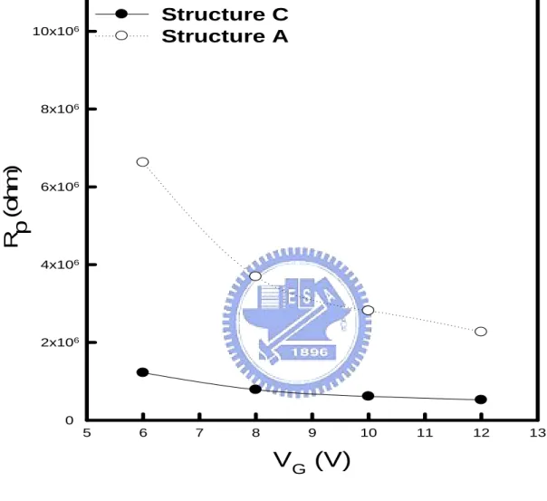
(44) Structure C Structure A. 10x106. Rp (ohm). 8x10⁶. 6x10⁶. 4x10⁶. 2x10⁶. 0 5. 6. 7. 8. 9. 10. 11. 12. 13. VG (V). Fig. 2-6. The gate voltage dependence of the parasitic resistance Rp of Structures A and Structure C.. 23.
(45) Fig. 2-7. The distribution of electrons near the drain region in the structures A. The arrow heads labeled in the two figures present the carrier transport directions.. 24.
(46) . Fig. 2-8. The distribution of electrons near the drain region in the structures C. In the proposed structure, the electrons can transport though contacts, the side wall and the top contact of drain metal overlap region.. 25.
(47) 2 .1 x 1 0 -6. S tru c tu re A S tru c tu re C. Drain cruuent ID (A). 2 .0 x 1 0 -6. 1 .9 x 1 0 -6. 1 .8 x 1 0 -6. 1 .7 x 1 0 -6. 1 .6 x 1 0 -6. 1 .5 x 1 0 -6 0. 200. 400. 600. 800. 1000. 1200. S tre s s tim e (s e c ). Fig. 2-9 The evolution of conducting currents in TFTs during bias temperature stressing (BTS). The current of 200nA was conducted on Structure A and C at 60oC with the gate bias of 11.25 V and 9V, respectively.. 26.
(48) Drain Current I (A) D. 1 0. -5. 1 0. -6. 1 0. -7. 1 0. -8. 1 0. -9. 1 0. -1 0. 1 0. -1 1. 1 0. -1 2. 1 0. -1 3. 1 0. -1 4. 1 0. -1 5. -1 0. S t ru c t u r e S t ru c t u r e. -5. 0. A C. 5. 1 0. 1 5. V G (V ). Fig. 2-10 The ID-VG relationships of the TFTs after bias temperature stress. The threshold voltage shift of structure A and C is 1.75V and 0.75V, respectively.. 27.
(49) Chapter 3. Investigation of Poly-Silicon Thin Film Transistors with/without LDD Structure at Temperatures and under AC stress. 3.1 Introduction Poly-Silicon Thin film transistors (Poly-Si TFTs) have been wily applied on the flat-panel displays like AMLCD and AMOLED. The major advantages of poly-Si TFTs are the higher driving capability than the amorphous silicon devices, and the existence of complementary devices.[3.1-3.5] Taking advantage of these features, poly-Si TFTs can be used to incorporate the integrated peripheral driving circuitry and switching transistor in the same substrate for flat-panel displays.[3.6-3.7] The integration of driver circuits would reduce the assembly complication and cost dramatically. If the mobility of poly-Si TFTs is further increased, this poly-Si technology will realize the system on panel (SOP) which will integrate memory, CPU, and display.[3.8-3.9] TFT devices in functional circuits serve as the switches and suffer the high frequency voltage pulses. Previous research reports have shown a relationship between the creation of states and hot-carriers effect by performing DC stress.[3.10-3.13] The degradation mechanism of n-channel TFT under dynamic voltage stress, however, has not been clarified yet.[3.14-3.16] The degraded TFT will seriously influence the operation of the circuits. In addition, the dangling bonds in the grain boundaries in the poly-Si film serve as the trapping centers that play a cruel role for the electrical performance of poly-Si TFT. [3.17-3.18] These defect states in energy band gap would enhance the carrier to tunnel at the high field.[3.19-3.20] Therefore, the leakage current due to trap-assisted. 28.
(50) tunneling effect is much larger in poly-Si TFTs than in the single crystal MOSFETs. Trap-assisted tunneling effect is known to be strongly dependent on the electrical field. In order to reduce the horizontal electric field around a drain, the lightly doped drain (LDD) structure is widely used for poly-Si TFTs. Some reports have demonstrated that the light-drain doping (LDD) technology can effectively reduce the electric field at the drain region and suppress the leakage current. [3.21-3.22] It also can keep down the kink effect resulted from the impact-ionization of energetic carriers which usually leads to the undesirable effect in electrical characteristics of TFT. The LDD-structure, hence, is necessary for the application of poly-Si TFT, especially for the N-channel TFTs. Moreover, the large area electronics or the flat-panel displays comprised of poly-Si TFTs are used by peoples at the globe. Thus, the displays should keep the performances well at all kinds of the environments. Temperature usually influences the characteristics of solid-devices, and its relative effects are important for the application of Poly-Si TFT technology. In this chapter, the temperature effects on the n-type poly-Si TFT with/without LDD structure was firstly investigated. Then we observed the AC stress effects on n-channel poly-Si TFTs without LDD to clarify the degradation mechanism.. 3.2 Temperature Effects on Poly-Si TFTs 3.2.1 Device Fabrication. Top-gate structured poly-Si TFTs were fabricated on glass substrate by low-temperature processes. Buffer SiO2 films and 90nm-thick amorphous silicon films were deposited by plasma enhanced chemical vapor deposition (PECVD), and. 29.
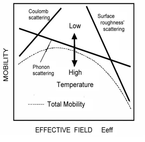
(51) subsequently, the films were dehydrogenated by furnace annealing. After dehydrogenation, the a-Si films were crystallized by XeCl excimer-laser. [3.23-3.24] The power of the line-shaped beam was 350 mJ/cm2. Following the laser process, 100nm-thick gate oxide was deposited by PECVD. Then the implantation was adapted to define the LDD region and S/D region. The LDD and S/D region was doped by phosphorous of 1 x 10¹³ atom/cm2 and 8 x 1014 cm3, respectively. Then MoW was sputtered as a gate metal. The LDD/gate overlap region is 0.75μm and LDD extends outside the gate 0.75μm. The dimension of the non-LDD TFTs in this section was W=12μm and L=6μm, the overlap of gate metal and S/D junction is 1μm. The cross section views of TFTs were illustrated in Figs. 3-1(a) and 1(b).. 3.2.2 Results & Discussions. Figure 3-2(a) shows the ID-VG relations and transconductance, gm, of poly-Si TFT at the temperatures from 50K to 250K. Figure 3-2(b) shows ID-VG relations in the linear scale.. The conducting current of STD TFT is significantly increased with the. decreasing of the temperature. The ON-current of TFT at 250K is 0.825 times that at the 50K. Moreover, the threshold voltage of the TFTs varied from 1.6V to 0.8V, extracted at current density of 10 nA with normalized channel width (W)/channel length (L) ratio. In figures 3-2(b), the maximum value of gm is also raised with the decreasing in temperature. The mobility extracted from the maximum value of gm is 135.8 cm2/Vs and 106.5 cm2/Vs at 50K and 250K, respectively. This phenomenon can be explained by the evolutions of the carrier scattering in poly-Si TFT at temperatures. Some reports have shown that the carriers in the MOSFET made on mono-crystalline silicon wafer suffer three types of scatterings, including impurity scattering, surface scattering and the phonon scattering, as shown in Fig. 3-3. [3.25] The phonon 30.
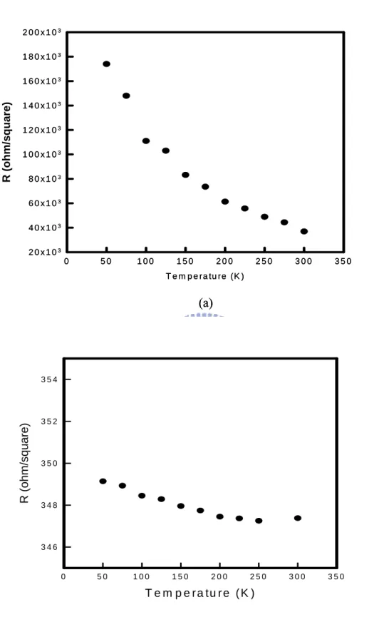
(52) scattering is due to the lattice vibrations and strongly dependent on the temperature. The carrier transport of poly-Si TFT is evidenced to be mainly limited by the grain boundaries in the poly-Si film.[3.26] However, the field effective mobility of carriers should be affected by the phonon scattering within the same boundaries in channel region. At high temperature, the carrier is seriously scattered by the numerous phonon. Accordingly, the effective mobility of carrier is lower at high temperature than that at low temperature. Unlike the MOSFET, the ELA poly-TFT owns lots of grain boundaries in the channel region. Thus, both the grain boundaries and phonons would deeply affect the carrier transport in the poly-Si TFT. Figure 3-4 illustrates the ID-VG relations of LDD-TFT at the temperatures from 50K to 250K. Unlike the non-LDD TFT, the conducting current of LDD TFT is decreased with the decreasing of the temperature. The dominant mechanism in conducting capability of LDD TFT at the low temperature should be different from the non-LDD TFT.. To clarify the difference between two devices, the sheet. resistances of phosphorous heavily-doped and lightly-doped poly-Si film are measured from 50K to 250K, demonstrated in Figs. 3-5 (a) and (b). It’s apparent that the resistivity of heavily-doped film almost keep well as the temperature changed. However, the LDD layer behaves as a temperature-dependent resistor which is a lager resistance at low temperature than at high temperature. The sheet resistivity of LDD at 50K is 4.72 times that at 300K. Since the LDD poly-Si sheet does not achieve the degeneracy doping level, the freeze effect of doped impurity atoms was observed. In addition, the traps of grain boundary play an important role for the conductivity of the poly-Si film. According to the Seto’s model, the electrons activated from the doped atoms, Phosphorous, were filled at the trap states at the grain boundaries. For simplify, the amount of free carrier in LDD layers, Nfree, can be equated to:. 31.
(53) +. N free = N D − N T. (1),. where ND+ is the number of ionized impurities and NT is the effective trap density. Thus, the conductivity of poly-Si film is proportional to the amount of free carriers. With the decreasing of the temperature, the amounts of activated electrons are decreasing and the ratio of trapped electrons is rising by assuming that the amount of trap states is non-varied. The few free electrons are contributed to the conduction, and thus the conductivity is decayed at low temperature. In heavily-doped poly-Si sheet, the amount of doped atoms is much larger than the trap density. Thus, the amount of activated electrons is much larger than the trap density in heavily-doped poly-Si sheet since the high doping level would lead to the degeneracy. Seto has shown that the resistivity of boron doped poly-Si film as a function of the doping level. At high doping level (Nd>>Nt), resistivity of poly-Si tends to approach the mono-crystalline one while the poly-Si may be degeneracy. Thus, heavily-doped poly-Si sheet exhibits the temperature-independent conducting behavior. Figure 3-6 schemes that LDD layers extended out the gate overlap region behave as the temperature-dependent resistors and series connecting with the gate control region. Although the conductivity of channel region is reversion to the temperature, the LDD sheets extended outside the gate electrode behave as the large resistors and limit the drain current.. 3.3 Electrical Degradation Mechanism of N-Channel Poly-Si TFT under AC Stress. 3.3.1 Device Fabrication Similar to the 3.2.1 section, the N-channel poly-Si TFT with top-gate structure were 32.
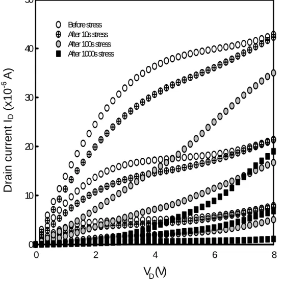
(54) fabricated on a glass substrate without lightly doped drain (LDD).. The dimensions. of TFTs in this work were L=9μm, W=6μm and the overlap of gate metal and S/D junction is 1μm. The cross section views of TFTs were illustrated in Fig. 3-7. The stress pulses were performed on the gate electrode as the dynamic stress and source/drain were grounded, as shown in the inset of Fig. 3-7. As for the stress condition, we used the rectangular pulse with amplifier of ±15V and frequency of 500kHz. Both the rising time (Tr) and falling time (Tf) were 100 ns.. 3.3.2 Results and Discussions. Figure 3-8 shows the ID-VG relationships of n-channel poly-Si TFT (L=9μm) with the dynamic stress times for 10 to 1000 s. The distinct decrease in on-current was found with the increasing stress duration. With the stress duration for 10 and 100 s, respectively, the conducting current of TFT operated at Vg=15V is 90% and 39% times of the magnitude of the initial value. After stressing for 1000 s, the on-current of TFT is degraded to 3% of the magnitude of the initial value. However, both the sub-threshold swing (0.28 V/dec.) and threshold voltage (2.41V) kept well during the stressing. From the evolution of the transfer characteristics at the linear operation region with stress time, it is apparent that the impact of the applied stress leads to a parallel decrease of the on-current operated at the above threshold region of the ID-VG characteristics. In poly-Si TFTs, the degradation under DC stress is usually characterized by a decrease of the sub-threshold slope mainly due to the generation of traps at deep states in poly-Si grains and a threshold voltage shift caused by charge trapping in the gate oxide and at the interface states. However, the experimental data showed that both subthreshold slope and threshold voltage remain unchanged in all stressed devices in comparison with the non-stressed device. This indicates that the 33.
(55) degradation of the n-channel poly-Si TFTs is neither occurred by charge trapping in the gate oxide nor by the creation of traps at the deep states. We can infer that the tail states produced by the strained bounding in poly-Si film are responsible for the electrical degradation of TFT. The ID-VD characteristics of TFT with the dynamic stress times are illustrated in Fig. 3-9. It is observed that the current crowding effect on TFT is significantly enlarged with the increase of stress time. Figure 3-9 also indicates parasitic resistance is contributed to the degradation on electrical properties of TFT. The parasitic resistance is dependent on the following several factors, such as the trap states near the source/drain junctions, sheet resistance of n+ poly-Si layer, and source/drain contact quality. For a constant W/L ratio, the effect of parasitic resistance can be clearly seen in the output characteristics of TFTs. The large parasitic resistance would result in the current crowding effect, as shown in Fig. 3-9. Under the operation of small drain voltages VD and high gate voltages VG, it can be assumed that the turn-on resistance Ron of TFT device consists of the channel resistance Rch and the parasitic source/drain resistance Rp. Ron = Rch+Rp , and Rch =. L WμC i (VG − VT ). (1). where Ci is the gate oxdie capacitance per unit area and W, L, and Vt are the intrinsic device channel width, length, and the threshold voltage, respectively. The parasitic resistance RP of TFT can be extracted through measuring the ON resistance Ron from the linear region of TFT output characteristics and through plotting the RonW against the channel length L. To extract the RP, we performed the dynamic stresses on the lengths of TFT for 3 μm, 6μm, 9μm, 10μm, 12μm and 30μm with the same stress conditions. The degradation phenomena of stressed TFTs are similar to the Figs. 3-8 and 3-9. Figure 3-10 illustrates the typical gate voltage dependence of the. 34.
數據
+7
相關文件
To stimulate creativity, smart learning, critical thinking and logical reasoning in students, drama and arts play a pivotal role in the..
Building on the strengths of students and considering their future learning needs, plan for a Junior Secondary English Language curriculum to gear students towards the learning
Promote project learning, mathematical modeling, and problem-based learning to strengthen the ability to integrate and apply knowledge and skills, and make. calculated
Building on the strengths of students and considering their future learning needs, plan for a Junior Secondary English Language curriculum to gear students towards the
Language Curriculum: (I) Reading and Listening Skills (Re-run) 2 30 3 hr 2 Workshop on the Language Arts Modules: Learning English. through Popular Culture (Re-run) 2 30
Wang, Solving pseudomonotone variational inequalities and pseudocon- vex optimization problems using the projection neural network, IEEE Transactions on Neural Networks 17
Define instead the imaginary.. potential, magnetic field, lattice…) Dirac-BdG Hamiltonian:. with small, and matrix
These are quite light states with masses in the 10 GeV to 20 GeV range and they have very small Yukawa couplings (implying that higgs to higgs pair chain decays are probable)..
