國立交通大學
電子工程學系 電子研究所碩士班
碩 士 論 文
萃取接觸阻抗係數方法之比較研究
──CBKR結構與改良式TLM結構
A Comparison Study of the Specific Contact
Resistivity Extraction Methods: CBKR Method
and Modified TLM Method
研究生:曾炫滋
指導教授:崔秉鉞 教授
萃取接觸阻抗係數方法之比較研究──CBKR
結構與改良式TLM結構
A Comparison Study of the Specific Contact
Resistivity Extraction Methods: CBKR Method and
Modified TLM Method
研究生:曾炫滋 Student : Hsuan-Tzu Tseng
指導教授:崔秉鉞
Advisor : Bing-Yue Tsui
國立交通大學 電子工程學系 電子研究所
碩士論文
A thesis
Submitted to Department of Electronics Engineering & Institute of Electronics College of Electrical Engineering and Computer Science
National Chiao Tung University in Partial Fulfillment of the Requirement
for the Degree of Master in
Electronic Engineering 2012
Hsinchu, Taiwan, Republic of China
i
萃取接觸阻抗係數方法之比較研究──CBKR
結構與改良式TLM結構
研究生:曾炫滋 指導教授:崔秉鉞
國立交通大學電子工程系 電子研究所碩士班
摘要
為提升積體電路之性能,金氧半場效電晶體的尺寸不斷微縮,金屬與源極和 汲極之接觸面積也隨之縮小,在相同接觸電阻係數下會導致較大的接觸電阻,甚 至可能限制藉微縮達成的性能提升。因此,如何降低接觸電阻係數成為首要之務。 而低接觸電阻係數的萃取亦是研究接觸電阻的一大課題。目前 廣為使用的 Cross-Bridge Kelvin Resistor (CBKR)結構其萃取誤差小,但仍會受製程限制造成 的寄生效應影響。Transmission line method (TLM)結構的製作方式簡單,但易受 製程變異影響也將造成萃取誤差。本論文提出一改良之TLM結構(Modified TLM, mTLM)並與CBKR結構相較,從模擬及實作探討此兩方法的準確度與極限。 過去已有文獻發表接觸電阻係數測量結構的二維模擬結果,近年亦有三維模 擬結構提出。文獻中藉由模擬提出接觸電阻係數萃取之數值分析解,藉以修正萃 取時測試結構造成的誤差。然分析解採用之模型通常經過簡化,且仍為一相當複 雜之關係式。因其需進行大量計算且只適用於特定狀況,對於真實情況下的接觸 電阻係數萃取僅能提供參考。因此,本論文使用三維數值模擬元件之電性以進行 接觸電阻係數之萃取。對CBKR結構而言,討論可能影響萃取結果之參數,其中 包含符合當今製程技術的測試結構尺寸。首先,縮小接觸窗可提升萃取之精確度; 其次,製程容忍度(δ)對萃取的相關性變低,此結論不同於二維模擬之結果。另 外,本模擬也將元件製作時可能遇到的問題列入考量。光學近接效應(opticalii
proximity effect)導致接觸窗的邊角圓化(corner rounding),造成萃取誤差增加。下 沉式接觸結構使等效接觸面積增加,並改變電流分布,因而低估接觸電阻係數。 至於mTLM結構,利用數值模擬設計結構尺寸後,同樣討論各參數對於萃取結果 的影響。因mTLM結構對製程變異甚為敏感,本論文從統計觀點研究其與載子濃 度分布變異及元件區側壁傾斜角度變異之相關性。結果發現mTLM結構對載子濃 度分布變異有高度相關,而元件區側壁傾斜角度變異之相關性則較輕微。另外, 同樣對mTLM考慮下沉式接觸結構,發現在接觸電阻係數較高時,接觸窗下沉會 造成接觸電阻係數的高估;而在低接觸電阻係數時則有低估的情形。 第二部分以實驗數據對照模擬結果。為能明確定義出元件區,元件之間採用 淺溝渠隔離技術(STI),在同一製作流程下完成CBKR和mTLM兩種測試結構。 CBKR萃取方式簡單,但寄生電阻的影響將導致無法避免之萃取誤差;mTLM萃 取過程相對複雜,但透過大量數據平均值趨近期望值之概念,可將其對製程變異 的敏感度降低,進而提升萃取的精確度。 本論文從模擬和實驗兩方面討論CBKR和mTLM兩種萃取接觸電阻係數之 方法。當CBKR隨著元件微縮而有較小之接觸窗,理論上可得較精確的萃取結果, 但寄生項的存在限制了萃取之精確度;而本論文提出之mTLM結構,使用STI技 術完成元件製作,利用平均化將其對製程變異敏感度降低之後,對於精確萃取接 觸電阻係數應具潛力。但若考慮下沉式接觸結構,其造成的影響複雜,對CBKR 和mTLM兩種結構都將產生無法預測之誤差。因此,透過本研究可看出接觸電阻 係數之萃取無論CBKR或mTLM兩種方法都遭遇困難,新穎結構與萃取方法仍為 迫切需求。
iii
A Comparison Study of the Specific Contact
Resistivity Extraction Methods: CBKR Method and
Modified TLM Method
Student: Hsuan-Tzu Tseng Advisor: Bing-Yue Tsui
Department of Electronics Engineering
Institute of Electronics
National Chiao Tung University
Abstract
To enhance the performance of Integrated circuits (IC), the MOSFETs have been scaled down continuously, and contact areas between metal and source/drain have shrunk consequently. Then, with a fixed specific contact resistivity (ρc), the contact
resistance increases and would suppress the performance improvement caused by scaling. Therefore, how to reduce the ρc is the first task, and how to extract such a low
ρc is also challenging. The Cross-Bridge Kelvin Resistor (CBKR) is a common used
test structure, which has a lower extracted error according to two-dimensional (2-D) analysis while the error still exists due to the parasitic effect caused by process limitation. The transmission line method (TLM) is easy to be fabricated but sensitive to the process variation. In this thesis, a modified TLM (mTLM) procedure is proposed and compared with the CBKR method by both simulation and experiment.
2-D simulations on the CBKR method have been widely studied, and three-dimensional (3-D) simulations have also been reported in recent years. Some
iv
analytic solutions were proposed to correct the extracted error. Nevertheless, as analytic methods are used, the models are usually developed after some simplifications, though still in a complex form. Thus, for a real case, analytic methods can only provide a rough estimation, since they have to perform complex calculation but only are suitable for particular conditions. In this thesis, 3-D simulation of device characteristics is performed to evaluate the accuracy of the ρc extraction by the CBKR
and mTLM methods.
For the CBKR method, several parameters are considered. The dimensions of the test structures are close to the design rule of the current IC technology. First, reducing the contact area will enhance the extraction accuracy. Second, the process tolerance (δ) has less influence on the extraction, which is different from the fact presented in 2-D simulation. Moreover, issues occurring in fabrication are also taken into account. The corner-rounding contact resulting from the optical proximity effect increases the extraction error. The recessed contact structure underestimates the ρc because of the
increase of the effective contact area and the change of the current distribution. As for the mTLM method, the dimensions of the mTLM structure are designed and optimized by simulation at first. Because the mTLM structure is sensitive to the process variation, this thesis studies the dependence on the variation of the dopant concentration and the variation of tapered sidewall angles of the active region according to the statistic. It is observed that there is a strong dependence on the variation of the dopant concentration, while a relative slight dependence on the variation of tapered sidewall angles of the active region. In addition, as the recessed contact is considered, the ρc is overestimated with higher ρc but underestimated with
lower ρc.
The second part shows the experimental data compared with the simulation. In order to define the active region explicitly, shallow trench isolation (STI) is utilized.
v
The CBKR and the mTLM structures are realized in an identical process flow. The CBKR method is easier to extract the ρc, but the parasitic resistance is about to result
in inevitable extracted error. The mTLM method is complicated; however, its sensitivity to the process variation could reduce and the extracted accuracy could be enhanced, by means of averaging sufficient data according to the fact that the average of sufficient data is closed to the expected value which is the true ρc.
This thesis discusses the CBKR and mTLM methods to extract the ρc by
simulation and experiment. The CBKR structure with a smaller contact area due to the devices scale down would obtain more accurate results in theory, while the parasitic resistance would still limit the accuracy. On the other hand, the mTLM structure proposed in this thesis is realized by using the STI process. Its sensitivity to the process variation could be diminished by averaging data. Therefore, the TLM method could be more accurate and is promising for ρc extraction. However, if the recessed
contact structure is considered, due to its complex influence on the ρc extraction, an
incalculable error would be caused for the CBKR and mTLM methods. Therefore, according to this thesis, it would be observed that the ρc extraction encounters great
challenge for both CBKR and mTLM methods. Novel test structure and extraction procedure are still critical issue.
vi
致謝
研究所的日子,無論學業、研究或者生活都學到許多,在此向曾幫助過我的 人們獻上由衷感謝。 首先最感謝的是指導教授 崔秉鉞老師,在老師悉心指導下,無論實驗分析 數據及呈現,或是做學問的態度,都讓我獲益良多。而在待人處事上,老師正直 而不失圓融的性格更讓我習得許多寶貴的經驗。 實驗方面感謝交大奈米中心與國家奈米元件實驗室提供製程機台與實驗環 境。特別感謝 NDL 的林家毅先生提供 STI 相關製程的協助,以及彭馨誼小姐在 磷酸濕蝕刻的幫忙。 感謝實驗室的大家,尤其感謝振銘學長在實驗與生活上的幫忙及關心。感謝 培宇學長在模擬的協助與建議,感謝嶸健學長與元宏學長幫忙 TEM 試片製作, 也感謝定業學長實驗與修課時的幫助,以及璽允學長在實驗室帳務交接時的幫忙。 謝謝子瑜在我研究上給我的支持,謝謝高銘鴻、茂元在實驗及量測上的幫忙,也 謝謝克勤、孫銘鴻的相互勉勵。謝謝哲儒平時的熱心,謝謝崇德常常提供新點子, 也謝謝雪君、翰奇、泰源和國丞帶給實驗室熱絡的氣氛。 感謝我的朋友們,研究之餘陪我聊天、給我加油打氣,最後感謝我的父母與 弟弟給我的支持,謝謝你們。vii
Contents
Abstract (Chinese) ... i
Abstract (English) ... iii
Acknowldegdments ... vi
List of Figures ... ix
Chapter 1 Introduction ... 1
1-1 Overview ... 1
1-2 Properties of Metal/Semiconductor Contacts ... 3
1-2-1 The Schottky Model of Metal/Semiconductor Contacts ... 3
1-2-2 Conduction Mechanisms for Metal/Semiconductor Contacts ... 4
1-3 Specific Contact Resistivity (ρc) ... 5
1-4 Measurement of Contact Resistance and Specific Contact Resistivity ... 7
1-4-1 The Transmission Line Model (TLM) ... 7
1-4-2 The Cross-Bridge Kelvin Resistor (CBKR) ... 10
1-5 Motivation ... 11
1-6 Thesis Organization ... 13
Chapter 2 Simulation Configurations, Results and Discussion ... 22
2-1 Overview ... 22
2-2 Device Structures and the Measurement Description of the CBKR Method ... 22
2-3 Device Structures and the Extraction Procedure of the Modified Transmission-Line Model (mTLM) Method ... 23
2-3-1 Device Structures of the mTLM Method ... 23
2-3-2 Extraction Procedure of the mTLM Method ... 24
viii
2-5 Simulation Results ... 25
2-5-1 Three-Dimensional Simulation of the CBKR Structure ... 27
2-5-2 Issues of the CBKR Structure ... 29
2-5-2-1 Considering the Circular Contact... 29
2-5-2-2 Considering the Recessed Contact ... 30
2-5-3 Three-Dimensional Simulation of the Self-Aligned mTLM Structure 31 2-5-4 Issues of the mTLM Structure ... 33
2-5-4-1 Considering the Variation of Doping Concentration in Semiconductors ... 33
2-5-4-2 Considering the Variation of Tapered Sidewall Angle of the Diffusion Region ... 34
2-5-4-3 Considering the Recessed Contact ... 36
Chapter 3 Experiments and Discussion ... 54
3-1 Overview ... 54
3-2 Experimental Settings of the CBKR Method and the mTLM Method ... 54
3-3 Process Flow ... 55
3-4 Results and Discussion ... 59
3-4-1 CBKR Method ... 59
3-4-2 mTLM Method ... 60
3-4-3 Comparison and Discussion ... 63
Chapter 4 Summary and Future Work ... 78
4-1 Summary ... 78
4-2 Future Work ... 81
References ... 83
ix
List of Figures
Chapter 1
Fig. 1-1 Components of the resistance associated with the source/drain junctions of a
MOS transistor [4]. ... 14
Fig. 1-2 Relative contribution from each component of the resistance to series resistance for different technology nodes [6]. ... 14
Fig. 1-3 Electron energy band diagrams of the metal/semiconductor contact according to the Schottky model, (a) before contact (b) after contact. ... 15
Fig. 1-4 Electron energy band diagram of n-type semiconductor with surface states. This diagram shows the Fermi-level pinning ... 15
Fig. 1-5 Conduction mechanisms for metal/semiconductor contacts, (a) thermionic emission (b) thermionic-field emission (c) field emission. ... 16
Fig. 1-6 Image force barrier lowering (IFBL). The peak of the barrier lowers down as the IFBL is considered [16]. ... 16
Fig. 1-7 The concept of 1-D transmission line model (TLM). ... 17
Fig. 1-8 Different measured positions of the voltages for the front resistance (Rf) and the end resistance (Re), respectively... 17
Fig. 1-9 The transmission line tap resistor (TLTR)... 18
Fig. 1-10 Extraction of the front resistance (Rf) from the Rtotal-Ld plot. ... 18
Fig. 1-11 The contact end resistance (CER). ... 19
Fig. 1-12 The cross-bridge Kelvin resistor (CBKR). ... 19 Fig. 1-13 The ρce as a function of the ρc using the self-aligned CBKR structure in 3-D
simulation. As the 3-D effect is considered, i.e., ρb.t ≠ 0, even though a
x
ignored. The ρb is the resistivity of the semiconductor active layer, and t is
the thickness of the semiconductor active layer [26]. ... 20 Fig. 1-14 TEM image of the cross section of the bird’s beak due to the lateral diffusion of LOCOS [29]. ... 20 Fig. 1-15 TEM image of the cross section of tapered sidewall of STI [30]. ... 21
Chapter 2
Fig. 2-1 The general 3-D simulated structures of the CBKR method. ... 39 Fig. 2-2 Definition of parameters for CBKR method (a) with a square contact, and (b)
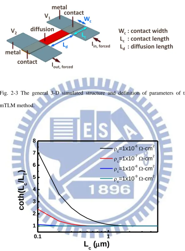
with a circular contact. The metal layer is not drawn here. ... 39 Fig. 2-3 The general 3-D simulated structure and definition of parameters of the
mTLM method. ... 40 Fig. 2-4 Design guideline of the Lc of the mTLM extraction procedure. The
coth(Lc/LT) approaches 1 as Lc >> LT. ... 40
Fig. 2-5 Simulated current distribution of the CBKR structure as δ = 0 using the CBKR structure. ... 41 Fig. 2-6 (a) Relative error versus the actual ρc with various Ac values as δ = 0 using
the CBKR structure. (b) Parasitic resistance versus the contact size with various ρc values as δ = 0 using the CBKR structure. ... 41
Fig. 2-7 (a) Relative error versus the actual ρc with various δ values as Ac = 50×50
nm2 using the CBKR structure. (b) Parasitic resistance versus the actual ρc
with various δ values using the CBKR structure. ... 42 Fig. 2-8 (a) Comparison of the relative error between the square contacts and the
circular contacts using the CBKR structure. The cases that δ = 0 and δ = 50 nm are both exhibited. (b) Comparison of the parasitic resistance between the square contacts and the circular contacts using the CBKR structure. The
xi
cases that δ = 0 and δ = 50 nm are both exhibited. ... 43 Fig. 2-9 Cross-section diagram of total S/D resistance with the recessed silicide taken
in account. The contact resistance includes two parallel components: the resistance underneath the silicide and the resistance at the side of the
recessed contact [67]. ... 44 Fig. 2-10 Relative error versus the recession depth with various ρc as Ac = 50×50 nm2
using the CBKR structure. ... 45 Fig. 2-11 Relative error versus the recession depth with various ρc as Ac = 1×1 μm2
using the CBKR structure. ... 45 Fig. 2-12 Extraction procedure of the ρc using the mTLM structure with Wc = 1 μm
and Lc = 2 μm as ρc = 1×10⁻⁷ Ω-cm2. (a) The Rf is obtained from the
y-intercept of the Rtotal-Ld plot. (b) The ρc is extracted from the slope of the
Rf-1/Wc plot. ... 46
Fig. 2-13 Relative error versus the actual ρc with different Lc using the mTLM
procedure... 47 Fig. 2-14 (a) Comparison of the relative error between the CBKR and mTLM
methods. Fig. 2-14(b) Comparison of the accuracy between the CBKR and mTLM methods. ... 47 Fig. 2-15 Distribution of the Rtotal values for each diffusion length (Ld) as the variation
of doping concentration in semiconductors is considered. For each Ld, 100
test structures are used with the doping concentrations of top surface set 1×1020 cm-3 ± 5% in Gaussian distribution. ... 48 Fig. 2-16 (a) Rf extrapolated from the intercept of Rtotal-Ld plot involving 100
extraction results. The Rf varies in a wide range, and Rf < 0 may even occur.
Fig. 2-16(b) Distribution of the Rs involving 100 extraction results from the
xii
considered. (c) Distribution of the Rf involving 100 extraction results from the y-intercept of the Rtotal-Ld plot as the variation of doping concentration
is considered. For certain cases, Rf < 0 occurs, which is impossible to
happen in reality. ... 49 Fig. 2-16(d) Distribution of the ρce involving 100 extraction results from the mTLM
method as the variation of doping concentration is considered. The inset shows the data in the range from 0 to 2×10⁻⁸ Ω-cm2 in detail. ... 50 Fig. 2-17 Distribution of the Rtotal values for each diffusion length (Ld) as the variation
of tapered sidewall angles of the diffusion region is considered. For each Ld,
100 test structures are used with sidewall angles set 88 ± 2° in Gaussian distribution. ... 51 Fig. 2-18 (a) Distribution of the Rs involving 100 extraction results from the slope of
the Rtotal-Ld plot as the variation of tapered sidewall angles is considered. (b)
Distribution of the Rf involving 100 extraction results from the slope of the
Rtotal-Ld plot as the variation of tapered sidewall angles is considered. (c)
Distribution of the ρce involving 100 extraction results from the mTLM method as the variation of tapered sidewall angles is considered. ... 51 Fig. 2-19 (a) Relative error versus the recession depth with different ρc values using
the mTLM structures. (b) The difference between the ρce and ρc versus the
recession depth with different ρc values using the mTLM structures. The
inset shows the results as ρc from 1×10⁻⁶ to 1×10⁻⁹ Ω-cm2 in detail.. ... 53
Chapter 3
Fig. 3-1(a) Schematic layout of test structures. (b) Schematic cross-section of test structures. Left: the mTLM method. Right: the CBKR method. ... 65 Fig. 3-2 Process flow of test structures. (a) Pad oxide growth and nitride deposition.
xiii
(b) Trench etching. (c) PECVD TEOS oxide deposition for trench filling. (d) CMP process. (e) Post-field oxidation process to finish STI. (f) BF2+
implantation and dopant activation. (g) Passivation oxide deposition and contact hole patterning. (h) NiSi silicidation. (i) Al pad patterning and Al sintering... 66 Fig. 3-3 (a) SEM image of the edge between STI and active region after CMP process. (b) OM image of the top view of the active region and dummy patterns after CMP process. The magnification is 1000x. (c) OM image of the top view of the mTLM structure after silicidation process. The magnification is 1000x. (d) OM image of the top view of the final mTLM structure. The
magnification is 250x. (e) OM image of the top view of the final CBKR structure. The magnification is 250x. ... 69 Fig. 3-4 (a) The ρce versus the Ac using the CBKR method with δ = 50 nm. The lowest
extractable ρce value is marked for each test structure with different Ac.
(b) The ρce versus the Ac using the CBKR method with δ = 0.1 μm. The
lowest extractable ρce value is marked for each test structure with different
Ac. (c) The ρce versus the Ac using the CBKR method with δ = 0.3 μm. The
lowest extractable ρce value is marked for each test structure with different
Ac. ... 72
Fig. 3-5 Illustration of two different forced current directions used in the CBKR extraction... 73 Fig. 3-6 Illustration of the Rf extrapolation from different groups of devices using the
mTLM method with Wc = 1 μm and Lc = 2 μm... 74
Fig. 3-7(a) Rf extrapolation after averaging Rtotal values for each Ld using the mTLM
method with Wc = 1 μm and Lc = 2 μm. Rf extrapolation after averaging
xiv
= 2 μm. (b) Rf extrapolation after averaging Rtotal values for each Ld using
the mTLM method with Wc = 1.5 μm and Lc = 2 μm. Rf extrapolation after
averaging Rtotal values for each Ld using the mTLM method with Wc = 1.5
μm and Lc = 2 μm. (c) Rf extrapolation after averaging Rtotal values for
each Ld using the mTLM method with Wc = 2 μm and Lc = 2 μm. ... 74
Fig. 3-8 (a) The ρce = 2.9×10⁻⁷ Ω-cm2 is extracted using the mTLM method with Lc =
2 μm. The ρce = 9.8×10⁻⁷ Ω-cm2 is extracted using the mTLM method with
Lc = 1 μm ... 76
Fig. 3-8(b) The ρce = 9.8×10⁻⁷ Ω-cm2 is extracted using the mTLM method with Lc =
1 μm. ... 76 Fig. 3-9 TEM images of NiSi/Si contact. Some unexpected voids between the NiSi
layer were observed, and thus the actual Ac should be smaller than the
1
Chapter 1
Introduction
1-1 Overview
Due to the requirement of higher device performance, scaling down is necessary to obtain larger driving current of transistors. However, there are some issues associated with continued CMOS scaling, such as gate dielectric leakage, parasitic capacitance, and parasitic series resistance [1-5]. The use of alternative high-κ gate dielectric materials would reduce gate leakage [6], and the reduction of the source/drain extension junction depth could decrease capacitive coupling of the drain to the channel. As for the parasitic series resistance, it is still a challenge and needed to be improved. As illustrated in Fig.1-1, the parasitic series resistance has been modeled by dividing into four components: source/drain extension (SDE) to gate overlap resistance Rov; SDE resistance Rext; deep S/D resistance Rdp; and
silicide-diffusion contact resistance Rc [7]. Among these components, the Rc varies as
a reciprocal to the scaling factor [8], and indeed it is predicted to dominate the total parasitic resistance of the device for future technology scaling, as shown in Fig.1-2 [9-12]. Therefore, the Rc should be emphasized on and will be investigated in
subsequent contents.
In order to characterize the contact resistance, contacts should be considered first. The metal/semiconductor contact is mainly concerned because it is most common. It was discovered by Braun in 1874, and the first acceptable theory was developed by Schottky in the 1930s, which is frequently referred as Schottky model [13]. According to the basis of semiconductor device physics, conduction mechanisms for
2
metal/semiconductor contacts will be discussed briefly in section 1-2.
Considering the influence of the contact resistance to advanced devices, for multiple-gate transistors (MuGFET), it has been shown that the contact resistance between the S/D silicide and Si-fin dominates the S/D parasitic series resistance behavior of the narrow fin devices [14]. SiGe S/D, NiPt germanosilicide, and NiAl-alloy have been proposed to alleviate the concerns of the S/D parasitic series resistance in p-channel transistors [15-17]. For ultra-thin-body (UTB) SOI MOSFETs, the thin Si layer is the major cause of the increase of the parasitic series resistance. Thus the contact resistance plays a minor role in the parasitic series resistance and could be reduced by the silicidation of the source/drain to compensate for the increased parasitic resistance [4,18,19]. To reach a low parasitic S/D contact resistance, the Schottky-barrier (SB) MOSFET devices would be attractive. By replacing the S/D impurity doping with metal-like silicides typically, the SB MOSFET provides an elegant solution to reach a low parasitic S/D contact resistance, although for the SB CMOS circuits there are requirements that a silicide for NMOS having a low barrier to electrons on N-type silicon and another silicide for PMOS having a low barrier to holes on P-type silicon [20].
Owing to the significance of the contact resistance to devices, an appropriate parameter should be introduced to describe the contact characteristics. Then, the specific contact resistivity (ρc), which is independent of contact size (Ac), is
introduced. Ideally the current drive in a MOSFET is limited by the channel resistance, while in practice all components of the parasitic series resistance illustrated in Fig.1-1 have great influence and would suppress the device performance. The requirement that the summation of these other resistances should be less than 10% of the channel resistance for normal design procedures determines the demand of the ρc, which
3
Roadmap of Semiconductor (ITRS) [21].
For such a low value, how to accurately extract ρc should be carefully considered.
Typical measurement methods are described in section 1-4. Because the extracted specific contact resistivity (ρce) becomes erroneous, a new extraction procedure using
modified transmission line model (mTLM) is developed and compared with the common used cross-bridge Kelvin resistor (CBKR) method in this thesis. Finally, the outline of this thesis is given.
1-2 Properties of Metal/Semiconductor Contacts
1-2-1
The Schottky Model of Metal/Semiconductor Contacts
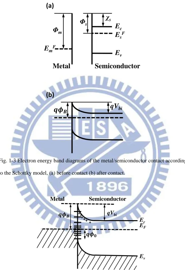
The energy band diagrams of a metal/semiconductor contact according to the Schottky model is shown in Fig.1-3. When a metal contacts with a semiconductor, intimate contact between the two materials are assumed. There are some parameters to be introduced. The metal work function (ΦM) is the energy difference between the
Fermi level and the vacuum level of the metal; the semiconductor work function (ΦS)
is defined similarly; the relationship between a work function and its correlated potential is 𝜙𝑀 =𝛷𝑞𝑀; the electron affinity (χs) is the potential difference between the
bottom of the conduction band and the vacuum level at the semiconductor surface. For the case that an n-type semiconductor meets a metal with higher work function, electrons pass from the semiconductor into the metal. The resulting potential difference is the built-in potential (Vbi), which is the difference between ΦM and ΦS.
The barrier height (ϕB) after contact is given by 𝜙𝐵 = 𝜙𝑀− 𝜒. Vbi and ϕB are shown
in Fig.1-3.
According to the equation above-mentioned, barrier height (ϕB) is strongly
4
predominantly ionic semiconductors the strong dependence can be observed. Bardeen first explained the insensitivity of barrier height to the metal work function in covalently bonded semiconductors. It is indicated that the localized surface states determine the barrier height. Dangling bonds increase localized energy states at the surface of the semiconductor with energy levels lying in the energy gap. These surface states distribute continuously in the band gap and are characterized by a neutral level (ϕ0), as shown in Fig.1-4. The surface states modify the charge in the depletion region
and thus influence the barrier height. If there is a higher density of surface states at the semiconductor surface, charge exchange happens mostly between the metal and the surface states, rather than between the metal and the semiconductor. As a result, the barrier height in Fig.1-4 becomes independent of the metal work function, which is called the Fermi-level pinning [22].
1-2-2
Conduction Mechanisms for Metal/Semiconductor Contacts
The conduction mechanisms for a metal/semiconductor contact are illustrated in Fig.1-5(a), (b), and (c) [13,23]. Thermionic emission dominates when the barrier width is so wide that electrons can only jump over the barrier by thermal excitation. This occurs for lightly-doped semiconductors. The current density dominated by thermionic emission is given by
𝐽 = 𝐴∗𝑇2𝑒𝑥𝑝 (−𝑞𝜙𝐵
𝑘𝑇 ) (𝑒𝑥𝑝 (
𝑞𝑉
𝑘𝑇) − 1),
(Eq. 1-1) where A* is the Richardson’s constant, k is the Boltzmann constant, and T is the absolute temperature.
Field emission means carrier tunneling directly because the barrier is sufficiently narrow. This mechanism takes place when the semiconductor is high-doped. The
5
tunneling current can be described by
𝐽 ∝ 𝑒𝑥𝑝 (−𝑞𝜙𝐵 𝐸00 ),
(Eq. 1-2) where E00 is the characteristic energy, which is defined by
𝐸00 = 𝑞ℏ 2 √ 𝑁 𝑚∗𝜀 𝑠,
where ħ is the Plank constant, N is the dopant concentration, m* is the tunneling effective mass, and εs is the permittivity of a semiconductor. The image force barrier
lowering (IFBL) is also an effect depending on the doping concentration. When an electron in the semiconductor is at a distance x from the metal, there exists an electric field perpendicular to the metal surface. A hypothetical positive image charge q located at a distance (-x) inside the metal is assumed and therefore the electron has a negative potential energy
𝐼𝐹𝐵𝐿(𝑥) = − 𝑞
2
16𝜋𝜖𝑑𝑥,
where 𝜖𝑑 represents the permittivity of the semiconductor. This potential energy should be considered to obtain the total energy of the electron. Fig.1-6 shows that the peak of the barrier is reduced consequently, and it is dependent on the electric field at the contact. The larger the electric field at the contact, the larger the barrier lowering by image force.
Thermionic-field emission basically combines thermionic emission with field emission, and it dominates the current density when the semiconductor is in the medium doped concentration.
1-3 Specific Contact Resistivity (ρc)
6
pass through the interface. The contact resistance is characterized by two quantities: the contact resistance, Rc (Ω), and the specific contact resistivity, ρc (Ω-cm2). The
definition of the ρc is the reciprocal of the derivative of current density to the voltage
at zero bias, as shown in the following expression: 𝜌𝑐 = (
𝜕𝐽 𝜕𝑉)𝑉=0
−1
(Eq. 1-3) The ρc is not a measurable parameter but can be calculated from the
corresponding Rc as
𝜌𝑐 = 𝑅𝑐𝐴
(Eq. 1-4) , where A (cm2) is the effective contact area. The ρc is a useful parameter to evaluate
ohmic contacts because of its independence of contact area. Therefore, the ρc can be
utilized simply to compare qualities of contacts with different contact sizes.
For semiconductors with lower doping concentrations, the current density of a metal-semiconductor contact is dominated by thermionic emission, given as in Eq. 1-1. Therefore, the corresponding ρc is derived as
𝜌𝑐(𝑇𝐸) = 𝑘
𝑞𝐴∗𝑇𝑒𝑥𝑝 (
𝑞𝜙𝐵 𝑘𝑇 )
(Eq. 1-5) On the other hand, for semiconductor with higher doping concentrations, tunneling process dominates the current density. The tunneling current is given as Eq. 1-2. Consequently, 𝜌𝑐(𝐹𝐸) ∝ 𝑒𝑥𝑝 ( 𝑞𝜙𝐵 𝐸00) = 𝑒𝑥𝑝 [ 2√𝜀𝑠𝑚∗ ℏ ( 𝜙𝐵 √𝑁𝑑 )] (Eq.1-6) Briefly, according these above equations, the ρc(TE) is sensitive to temperature for a
7
given barrier height, while the ρc(FE) is sensitive to the doping density under the
contact [13].
1-4 Measurement of Contact Resistance and Specific Contact
Resistivity
In order to obtain the ρc correctly, accurate model of contact resistance is
essential. In general, 3-dimensional (3-D) model is comprehensible. The contact system can be described sufficiently by the Poisson and the two carrier continuity equations. However, it is difficult for computation and generalization in the 3-D analysis. Then, some simplifications and boundary conditions are made and 2-D model, or even 1-D model, was achieved [24].
For the last thirty years, several test structures for ρc extraction have been
proposed. The two-terminal contact resistance method is the earliest and simplest method. However, it only provides the information of contact process quality but neither contact resistance nor the ρc value [13]. The transmission line model (TLM) is
a common method to extract contact parameters and then determine the ρc. Based on
the TLM, the front resistance (Rf) and the end resistance (Re) can be obtained
depending on measuring the voltage from different positions of the contact [25-27]. The cross-bridge Kelvin resistor (CBKR) is the most widely employed method because it can measure the ρc directly [25,28,29]. The vertical CBKR test structure
was proposed to minimize the lateral current crowding which is the difficulty that the typical CBKR encountered [30].
In the following subsections, the concepts of the TLM and the CBKR method are presented in detail.
8
The transmission line model (TLM) of the metal/semiconductor contact is introduced by Shockley and further refined by Berger [31]. The 1-D TLM is illustrated in Fig.1-7. The semiconductor is assumed with a distributed sheet resistance (Rs) and no thickness. On the other hand, the metal is assumed with a
negligible sheet resistance. By solving the Poisson and the continuity equation simplified in the 1-D model, current density is obtained from the TLM as follows:
𝐼(𝑥) = 𝐼1𝑒𝑥𝑝(−𝑥 𝑙⁄ ), 𝑡
(Eq. 1-7) where 𝑙𝑡= √𝜌𝑐⁄ is the characteristic length at which 63% of the current has 𝑅𝑠 transferred into the metal, and I1 is the initial current injecting at the leading edge of
the contact. It is noted that this model is valid when the contact length (Lc) is long, i.e.,
𝐿𝑐 ≫ 𝑙𝑡.
The operation of test structures based on the TLM approach is that a current I is injected into the contact from the diffusion to the metal, and the voltage between the two layers is measured by two other terminals. Different measured positions of the voltage are for the front resistance (Rf) and the end resistance (Re), respectively, as
shown in Fig.1-8.
The transmission line tap resistor (TLTR), as illustrated in Fig.1-9, is a convenient structure to measure the front resistance (Rf). In Fig.1-8, the Rf is defined
as the ratio of the voltage drop (Vf) across the interfacial layer at the front edge of the
contact to the total current through the contact [24,25]. At the front edge, the current density is the highest. The total resistance (Rtotal) between the two metal terminals
consists of the diffusion resistance between the two contacts and the Rf of both
contacts:
𝑅𝑡𝑜𝑡𝑎𝑙 = 𝑅𝑠× 𝐿𝑑
9
(Eq. 1-8) where Rs, Ld, and Wd are the sheet resistance, the length, and the width of the
diffusion region, respectively. By means of varying Ld, the Rf can be obtained, as
shown in Fig.1-10. In the 1-D model, the Rf is solved in the following form:
𝑅𝑓= 𝑉𝑓 𝐼 = √𝑅𝑠𝜌𝑐 𝑊𝑐 𝑐𝑜𝑡ℎ(𝐿𝑐⁄ ) 𝐿𝑇 (Eq. 1-9) and 𝐿𝑇 = √𝜌𝑅𝑐 𝑠, (Eq. 1-10) where Lc is the contact length, Wc is the contact width, and LT is the transfer length.
Hence the ρc can be extracted from the Rf.
The end resistance (Re) is defined as the ratio of the voltage drop (Vf) across the
interfacial layer at the rear edge of the contact to the total current through the contact [24,25]. At the rare edge, the current density is the lowest. Similar to the Rf,
𝑅𝑒 = 𝑉𝑒 𝐼 = √𝑅𝑠𝜌𝑐 𝑊𝑐 csch(𝐿𝑐⁄ ). 𝐿𝑇 (Eq. 1-11) The contact end resistance method (CER) is illustrated in Fig.1-11.
The great advantage of the TLM structure is its simplicity to be fabricated [32-34]. The 1-D analysis is based on the assumption that contact width and diffusion width are equal, i.e., Wc=Wd [35]. However, the condition is not in practice, and the
lateral current flows in the diffusion region around the contact, which results in errors when extracting the ρc employing the typical TLM [29,36]. Circular TLM(CTLM)
can avoid the extracted inaccuracy stemming from the lateral current [13,37,38]. Besides, the 2-D analysis has been studied [24,35,39]. If the thickness of the diffusion region is considered, the 3-D model is necessary.
10
fabrication process, i.e., the ρce not only varies with the contact size but also depends
on the Rs of the doped semiconductor layer [39]. Analytical model has been
developed for the experimental uncertainty from the fundamental TLM expressions [34,40,41].
1-4-2
The Cross-Bridge Kelvin Resistor (CBKR)
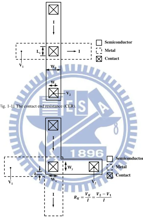
The cross-bridge Kelvin resistor (CBKR) is a widely used method to extract the ρc because it measures the ρc directly and simply [13,25,34,42]. Fig.1-12 shows a
general four-terminal CBKR structure with definitions of its geometry parameters. A current (I) is forced into one diffusion arm, through the contact, and then flows out the test structure from a metal arm. The voltage drop (Vk) of the interfacial region
between diffusion and metal is measured as V2-V1 by using other two voltage sensing
arms [25,28,31]. Then, the measured Kelvin resistance (Rk) is the ratio of the voltage
drop across the contact (Vk) to the current flowing through the contact, i.e.,
𝑅𝑘 =
𝑉𝑘
𝐼.
(Eq. 1-12) Then the ρc is extracted from the measured Kelvin resistance,
𝜌𝑐𝑒 = 𝑅𝑘𝐴.
(Eq. 1-13) As the ρc is large, it is valid according to the 1-D analysis [43] that the Rc equals
the Rk but current injecting into the overlap region (δ) between the contact edge and
the diffusion edge is not explained explicitly. For the ρc becomes smaller, the 1-D
model cannot describe the data correctly [24,43-45]. Therefore, the 2-D analysis is needed for extracting the ρc more accurately. Corrections for the extraction error have
been studied extensively by numerical simulations [24,44-46] and analytical modeling [36,43,47]. In the 2-D model [43], Rgeom, involving the current flow around the
11
contact in the overlap region, is introduced into one of the components of measured Rk, 𝑅𝑘 = 𝑅𝑐 + 𝑅𝑔𝑒𝑜𝑚, (Eq. 1-14) where 𝑅𝑔𝑒𝑜𝑚 = 4𝑅𝑠𝛿 2 3𝑊𝑥𝑊𝑦[1 + 𝛿
2(𝑊𝑥−𝛿)] and Rs is the sheet resistance of the underlying layer. Thus, Rk is dependent of Rs in the 2-D analysis and will affect the extraction of
the ρc. As the thickness of the semiconductor layer (l) is considered, 3-D analysis is
required [48,49]. In the 3-D analysis [49], the voltage drop at the metal-semiconductor interface is compared to that at the semiconductor, and the ratio will influence the determination of the ρc.
Universal error correction curves were provided in a number of previous works, in order to correct the systematic error in the CBKR [50]. Universal curves have been given by 2-D [24,51-53] and 3-D model [49]. In addition, random measurement error on the ρc extraction has been considered [50], and evaluation of the Ac has been also
studied [54,55].
1-5 Motivation
Although there have been reports that successfully obtained the ρce even in the
range of 10-10 Ω-cm2 of metal to metal or metal to silicide contact [56,57], the low ρc
extraction between silicide and silicon below 10-8 Ω-cm2 regime is still considered to
be difficult [29,44,49,50]. To investigate completely, a 3-D simulation of the CBKR structure is necessary to be performed, and the parameters should be reconsidered as well, including the case that the Ac reduces to achieve the design considerations of
nowadays as the ρc approaches to 10-8-cm2.
12
other test structures, such as the modified CBKR structure [58], the Scott TLM structure [33,60], and the end resistance method [59], have been studied. However, since the Scott TLM structure would suffer from an inaccurate estimation of current distribution [61] while the end resistance would be too low to be measured [24], the ρc
extraction should be still carefully considered. In this thesis, a modified extraction procedure using the transmission line model (mTLM) is proposed and studied by 3-D simulation.
It is expected that the extraction results of the fabricated test structures are consistent with those of the simulation. However, some parameters will affect the ρc
extraction during the fabrication, but they may not be easily analyzed in practice. It could be possible to infer their influences by the 3-D simulation results.
First, the sidewall tapered angles of the active region is needed to be discussed. As mentioned in section 1-4-1, Wd is larger than Wc in the TLM structure, which
results in additional error [35]. To achieve the self-aligned TLM structure, a novel process flow is proposed using the shallow trench isolation (STI), instead of the local oxidation of silicon (LOCOS) since the LOCOS incurs the lateral diffusion, as shown in Fig.1-14 [62], and cannot define the Wc exactly. As the STI structure is utilized, the
problem of lateral diffusion could be alleviated. Nevertheless, as shown in Fig.1-15, the sidewall would be not vertical entirely in practice [63], and thus could influence the ρc extraction.
Second, the doping concentration variation should be considered. In reality, some variations could occur in a fabrication process. Due to the sheet resistance is one of the essential parameters in the mTLM method [29], the variation of dopant concentration would degrade the accuracy of the ρc extraction.
Recession of the silicide is another problem of the ρc extraction. The silicon is
13
formed [42,57,64,65]. The sidewall of the recessed contact could be an additional current path [61,66,67], and hence the influence of the recessed contact of the CBKR and mTLM methods is needed to be studied.
Briefly, this thesis will focus on the comparison between the CBKR and mTLM methods, considering those above-mentioned problems.
1-6 Thesis Organization
The first chapter is the introduction consisting of properties of metal/semiconductor contacts, definition of the ρc, and common ρc extraction methods.
Besides, the mTLM method is also proposed. The second chapter presents the simulation configurations, results and discussion. Parameters are taken into considerations for the ρc extraction of both CBKR and mTLM methods, and the
influences of the issues during the fabrication process are also discussed. The process flow, experimental results and discussion are shown in the third chapter. Both the CBKR and mTLM structures are fabricated in an identical process flow, and their ρc
extractions are exhibited and compared with each other. During the extraction procedure there are some phenomena worthy to be discussed. The cross-section of the contact is also inspected by transmission electron microscopy (TEM) images. The last chapter is the summary and future works of this thesis.
14
Fig. 1-1 Components of the resistance associated with the source/drain junctions of a MOS transistor [4].
Fig. 1-2 Relative contribution from each component of the resistance to series resistance for different technology nodes [6].
15
Fig. 1-3 Electron energy band diagrams of the metal/semiconductor contact according to the Schottky model, (a) before contact (b) after contact.
Fig. 1-4 Electron energy band diagram of n-type semiconductor with surface states. This diagram shows the Fermi-level pinning .
E
mFE
vE
cE
sFΦ
mΦ
sχ
sMetal
Semiconductor
qV
bi(a)
(b)
Ev Ec EF Metal Semiconductor qVbi ++ + + + +
16
Fig. 1-5 Conduction mechanisms for metal/semiconductor contacts, (a) thermionic emission (b) thermionic-field emission (c) field emission.
Fig. 1-6 Image force barrier lowering (IFBL). The peak of the barrier lowers down as the IFBL is considered [16].
17
Fig. 1-7 The concept of 1-D transmission line model (TLM).
Fig. 1-8 Different measured positions of the voltages for the front resistance (Rf) and
the end resistance (Re), respectively.
I1-I2 Wd I1 I2 d Metal Interface layer Heavily doped region I(x) V(x) Ve I2 Vf G’ dx R’ dx I1 0 x I1-I2 = = I Metal Diffusion Wd Vf Ve = = = = Contact end Transmission line tap
18
Fig. 1-9 The transmission line tap resistor (TLTR).
Fig. 1-10 Extraction of the front resistance (Rf) from the Rtotal-Ld plot.
I I V1 V2 Ld Semiconductor Metal Contact Wd Wc Lc -2 0 2 4 6 8 0 400 800 1200 1600 2000 2400
R
to tal(
)
L
d(
m)
2R
fR
total=R
sx L
d/W
d+ 2R
fR
s=-2R
fx W
d/L
d19
Fig. 1-11 The contact end resistance (CER).
Fig. 1-12 The cross-bridge Kelvin resistor (CBKR).
I I V1 V2 Semiconductor Metal Contact Wc Wd Lc I I V1 V2 Semiconductor Metal Contact δ Wx Wy = = −
20
Fig. 1-13 The ρce as a function of the ρc using the self-aligned CBKR structure in 3-D
simulation. As the 3-D effect is considered, i.e., ρb.t ≠ 0, even though a self-aligned
CBKR structure is utilized, the parasitic resistance cannot be ignored. The ρb is the
resistivity of the semiconductor active layer, and t is the thickness of the semiconductor active layer [26].
Fig. 1-14 TEM image of the cross section of the bird’s beak due to the lateral diffusion of LOCOS [29].
21
22
Chapter 2
Simulation Configurations, Results and
Discussion
2-1 Overview
In this chapter, the device structure and the ρc extraction in simulation of the
CBKR method are introduced at first in section 2-2, and next those of the mTLM method are mentioned in section 2-3. Then, in section 2-4, the simulation settings of the ρc extraction for this work is presented. Finally, the simulation results for both the
CBKR and the mTLM method are shown and compared in section 2-5, which consists of the ideal and real conditions respectively.
2-2 Device Structures and the Measurement Description of the
CBKR Method
Fig.2-1 illustrates the generalized structure of the CBKR method for simulation by using a Sentaurus simulator in this work. In Fig.2-2(a), the contact width (Wc) and
the contact length (Lc) are the same for the square contact and the contact size (Ac) is
defined as Wc × Lc. For circular contact, the Ac is defined as π × (d/2)2, where d is the
diameter of a circular contact as shown in Fig.2-2(b). The lengths of the current carrying arm and the voltage sensing arm are more than two times of the Wc to
guarantee uniform current distribution as well as the accuracy of voltage sensing [29]. The process tolerances (δ) are assumed equal in x and y directions; besides, there is no misalignment considered in this work. The diffusion junction depth (xj) is set as
23
100 nm. The diffusion region is arsenic doped with Gaussian doping profile and the corresponding sheet resistance Rs is 217.82 Ω/□. The metal thickness is set as 100 nm,
and the sheet resistance is 0.245 Ω/□. The depth of contact interface (mj) is defined as
the depth of silicon consumption during silicidation and is measured from the Si surface.
The CBKR structures in this work include a wide range of contact sizes (Ac) for
the square contact: 1×1 μm2, 0.5×0.5 μm2, 0.1×0.1 μm2, 50×50 nm2, 40×40 nm2, 30×30 nm2, 20×20 nm2, and 10×10 nm2. As the circular contact is considered, the Ac
is determined by the diameter of the contact (d), and the d values are chosen to be the same as the Wc of square contacts. In addition, the process tolerances (δ) are
considered with 0 nm, 10 nm, 20 nm, 30 nm, 40 nm, and 50 nm. When the recessed contact is considered, moreover, the depths of contact interface (mj) are 10 nm, 20 nm,
30 nm, 40 nm, and 50 nm.
The measurement of the CBKR method has been explained in section 1-4-2, and Eq.1-12 and Eq.1-13 show the details of extraction procedure.
2-3 Device Structures and the Extraction Procedure of the Modified
Transmission-Line Model (mTLM) Method
2-3-1
Device Structures of the mTLM Method
Fig.2-3 illustrates the generalized structure of the mTLM method for simulation by using a Sentaurus simulator in this work. The mTLM method is on the basis of the transmission-line model (TLM) [31]. It should be noted that the diffusion width (Wd)
is in general larger than the contact width (Wc). However, in this thesis, that the Wd
equals the Wc would be achieved by a novel process flow with shallow trench
24
considered in the mTLM method. The contact length (Lc) is a critical factor in the
mTLM method for simplification and will be explained in detail in section 2-3-2. Besides, the Rs and the thicknesses of the diffusion region and the metal arms are set
to be the same as those of the CBKR method.
2-3-2
Extraction Procedure of the mTLM Method
In Fig.2-3, the total resistance (Rtotal) between any two contacts consists of the
diffusion resistance between the two contacts and the front resistance (Rf) of both
contacts, as mentioned in section 1-4-1:
𝑅𝑡𝑜𝑡𝑎𝑙 = 𝑅𝑠× 𝐿𝑑
𝑊𝑑+ 2𝑅𝑓,
(Eq. 1-8) where Rs is the sheet resistance of the diffusion region. The Rf can be extracted from
the y-intercept and the Rs can be extracted from the x-intercept of the Rtotal-Ld plot, as
presented in Fig.1-8. The correlation between the Rf and the ρc has been derived as
𝑅𝑓= 𝑉𝐼𝑓= √𝑅𝑊𝑠𝜌𝑐 𝑐 𝑐𝑜𝑡ℎ(𝐿𝑐⁄ ) 𝐿𝑇 (Eq. 1-9) and 𝐿𝑇 = √𝜌𝑅𝑐 𝑠 , (Eq. 1-10) where LT is the transfer length.
As Lc >> LT, the hyperbolic-cotangent term approaches 1 and then the Rf can be
simplified to: 𝑅𝑓 = 𝑉𝑓 𝐼 = √𝑅𝑠𝜌𝑐 𝑊𝑐 (Eq. 2-1) The slope of the Rf-1/Wc plot gives the ρc as the Rs is known. Fig.2-4 draws the
25
coth(Lc/LT) as a function of Lc with ρc as parameter and the Rs is 200 Ω/□. It is
observed that as ρc is lower than 1×10⁻⁷ Ω-cm2, the error becomes less than 0.1% if Lc
is longer than 1 μm. That is, the ρc can be extracted easily and accurately using
micro-process instead of nano-process. In this chapter, three Lc and Wc values of 1 μm,
1.5 μm and 2 μm are considered. In addition, several Ld values are used to obtain the
Rtotal-Ld plot.
2-4 Setting of Contact Resistivity (ρc)
In this simulation, the actual contact resistivity (ρc) is set by means of inserting
an extreme thin layer between the diffusion layer and the metal layer. Using the following relationship between the ρc and the resistivity (ρ) of this inserting layer:
𝜌𝑐
𝐴 = 𝜌 ×
𝐿 𝐴 ,
(Eq. 2-2) where A is the contact area and L is the thickness of the inserting layer. The actual ρc
values can be simply decided by setting appropriate resistivity values of the inserting layer as its thickness is chosen, for example 1 nm in this simulation.
For the recessed contacts, there are additional interfaces between the metal and the diffusion layer necessary to be taken into account. Side interfaces are added for both the CBKR method and the mTLM method. Similarly, extreme thin layers are inserted to set the ρc at the side interfaces as well as at the recessed interface.
2-5 Simulation Results
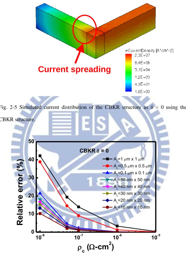
In this section, the simulation results of the CBKR method are discussed in section 2-5-1 and 2-5-2. At first, the 3-D effect is considered for the self-aligned CBKR structure. When the 3-D CBKR test structures are used, different contact sizes
26
(Ac) would affect the extraction accuracy. Next, the process tolerance (δ) is included
to describe the extraction of the CBKR method more completely. Thus, in section 2-5-1, the Ac and the δ dependence are shown. On the other hand, however, in reality
the CBKR method may suffer from some issues during the fabrication process. The contact shape would be closer to a circle due to the optical proximity effect especially when the contact size becomes smaller. Also, during the silicide formation, the recessed contact would be formed, causing the change of the extraction results and the current distribution as well. Section 2-5-2 will concentrate on these two situations, attempting to comprehend the extraction using the CBKR method in reality by analysis of simulation results.
The second part of this section discusses the mTLM method by simulation in section 2-5-3 and 2-5-4. In section 2-5-3, the simulation results of the optimum mTLM structures are shown at first, and then compared with the self-aligned CBKR method to figure out the intrinsic extraction error for each method. Then, it should be necessary to include some problems happening in reality too. Unlike the direct ρc
extraction of the CBKR method, the mTLM method would be more sensitive to the variation of fabrication process because of the needs of several test structures with different Ld for its extraction procedure. The Rs is determined by the distribution of
the doping concentration in the diffusion region. In addition, the current distribution would be affected by the sidewall angles of the STI structure as the STI process is utilized. In section 2-5-4, these two issues are analyzed by the statistic, observing the consequence if the mTLM method is used in reality. At last, the recession of the contact would be also a difficulty in the ρc extraction by the mTLM method and will
27
2-5-1
Three-Dimensional Simulation of the CBKR Structure
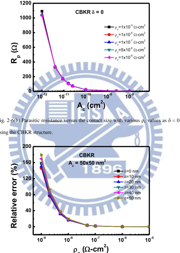
Traditional two-dimensional (2-D) model predicts that the extracted error depends on the process tolerance between contact hole and the diffusion region (δ), and the error becomes zero on self-aligned structure, i.e. δ = 0 [29]. However, when a 3-D structure is considered, the parasitic resistance cannot be ignored even though a self-aligned CBKR structure is utilized. Fig.2-5 shows the simulated current distribution of the CBKR structure as δ = 0. The thickness of the diffusion layer provides additional current path; hence the current crowding happens at both the underneath and the outside of the contact region and results in the parasitic resistance. This phenomenon is also shown in the literature [49]. In Fig.2-6(a), the relative error as a function of the actual ρc with various Ac is shown by simulating self-aligned
CBKR structures. It seems that the smaller Ac could help the ρc extraction more
accurate. To explain explicitly, the Ac dependence of the parasitic resistance should be
discussed first, illustrated in Fig.2-6(b). It is observed that the parasitic component (Rp)
increases as the contact size reduces, which is independent of the ρc value. Similar to
the 2-D model, the measured resistance (Rk) also suffers from the Rp, which involves
the current flow around the contact or under the contact since the depth of the diffusion region is taken into account for 3-D analysis. Hence, the Rp depends on the
properties of the diffusion layer like the sheet resistance or the depth. To concentrate on the Rp, as the current flows through the diffusion layer, if the contact size is smaller,
then the cross-sectional area where the current encountering would be smaller as well, and hence the parasitic resistance increases. Then, according to Eq.1-14, the ρc can be
deduced from the following equation:
𝜌𝑐𝑒 = 𝑅𝑘× 𝐴𝑐 = 𝜌𝑐 + 𝑅𝑝× 𝐴𝑐
(Eq. 2-3) Since the amount of the Rp increasing is less than that of the Ac decreasing, the
28
parasitic term in Eq.2-3 diminishes with the decrease of the Ac, and therefore the ρc
can be extracted more accurately as the Ac reduces.
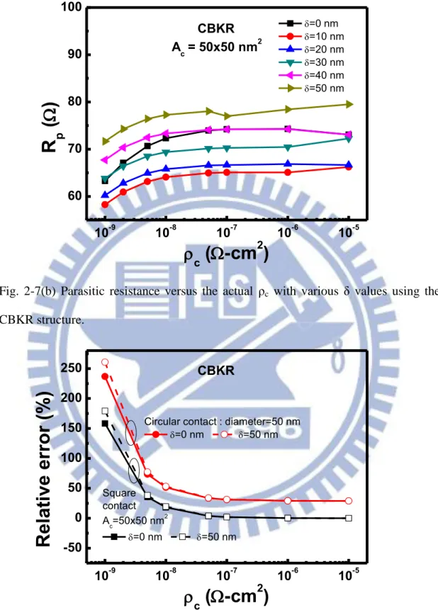
Fig.2-7(a) shows the δ dependence of the CBKR method in the ρc extraction as
the Ac reduces to 50×50 nm2. Similarly, the parasitic resistances are illustrated in
Fig.2-7(b) to realize the influence of the δ. In previous 2-D simulation results, the δ is regarded as a critical error source for the CBKR method [29]. The fact that the extraction error becomes higher as the δ increases is also mentioned in the literature. On the contrary, the influence of the δ is more complicated in the 3-D simulation. When the test structure is no longer self-aligned, i.e., δ ≠ 0, the Rp decreases at first,
and then increases with the δ. The decrease of the Rp could be explained by the
restriction against current crowding outside the contact at the voltage arm, due to the additional corner formed by the δ between the voltage arm and current arm of the diffusion region. Then, with the increase of the δ, more additional current paths are provided near the contact, which weakens the restriction from the corner formed by the δ and hence raises the Rp. In addition, it is noticed that for the structures with δ = 0
and δ ≠ 0, δ = 10 nm for example, the Rp difference between these structures is less
for higher ρc than that for lower ρc. It should be mentioned first that the current could
flow into the contact easier as ρc decreases, which reduces the current crowding effect
near the contact region. This could be observed as the ρc is below 10-7 Ω-cm2 in this
simulation, and therefore the Rp diminished gradually. Then the δ dependence is
considered. The δ restricts the current crowding outside the contact; however, it has a weak influence on the cases with a lower ρc, since the current tends to flow into the
contact already, and consequently the decrease of the Rp is less. It should be noticed
that although the Rp values are different for each ρc in Fig.2-7(b), there is a lightly
effect on the ρcedue to the product with relative small Ac value based on Eq.2-3. Thus,
29
2-5-2
Issues of the CBKR Structure
2-5-2-1 Considering the Circular Contact
Ideally the printed features should conform to the design patterns, i.e., for the general CBKR structures, contacts would be square-shaped. Nevertheless, due to the optical proximity effect, feature distortion occurs in the pattern transfer process, and problems like pitch effect, line-end shortening, and corner rounding are commonly observed [2]. Among the above-mentioned effects, corner rounding would change the actual contact sizes of the CBKR structures, and make an obvious difference to the extraction accuracy. In this subsection, the CBKR structures with the circular contacts, which can be seen as the worst case affected by corner rounding, are discussed.
The CBKR structures with the circular contacts have been studied in the literature [57], though only the 2-D model was considered. In this work, 3-D simulation is performed for the circular contacts with d=50 nm and the square contact with Ac=50×50 nm2. The comparison of the relative error between square contacts and
circular contacts using the CBKR structures with both δ = 0 and δ = 50 nm is shown in Fig.2-8(a), and the Rp values are shown in Fig.2-8(b). First of all, in the two figures,
curves can be divided into two groups by different contact shapes, indicating that the contact shape plays a major role on the parasitic resistance instead of the δ. It seems that both of the circular contact and the δ provide paths for current flowing through, but essentially the two cases are different. Referring to the circular contact, the current prefers to flow through the middle of the current arm into the contact due to the relative shorter distance to the contact rather than the sides of the current arm. Then, near the contact region, the current would flow into a narrow path, enhancing the current crowding effect at the front end of the circular contact and nearby region. In contrast with additional nearby current path due to the δ, the circular contact directly changes the current distribution. Thus, the Rp caused by the circular contact is
30
remarkably larger than that by the δ, shown in Fig.2-8(b). Furthermore, the trend that the Rp decreases with the ρc for the circular contact is also observed. As the ρc is
higher, current crowding effect near the contact is more serious for the circular contact, which leads to a significant difference between the results of the circular contact and of the square contact. By contrast, as the ρc decreases, because of the shortening of the
transfer length, test structures with both the circular and the square contacts suffer from the current crowding effect too, and therefore the difference between the two kinds of contact shape reduces.
2-5-2-2 Considering the Recessed Contact
To analyze simply, only the elevated silicide/Si contacts, i.e., mj = 0, are
considered in previous subsections. However, in the real case, during the silicide formation, silicon is consumed and the recessed contact between silicide and silicon would be formed. It is generally believed that as the consumption of silicon increases during the silicide formation, the contact series resistance is susceptible to increase due to the decrease in active dopant concentration at the silicide/Si interface or increase in sheet resistance underneath silicide [68]. In addition, there is another current path at the side of recessed contact region which is being parallel with current flow at the contact under silicide layer, as illustrated in Fig.2-9 [67]. Briefly, as the recessed contact is taken into account, the current distribution would be different, and details are about to be described in this subsection.
Fig.2-10 and Fig.2-11 shows the relative error as a function of the recession depth with different ρc for Ac = 50×50 nm2 and 1×1 μm2. It is observed that in both
figures the ρce becomes smaller as the recession depth increases, even lower than the
actual ρc value. It could be explained by the enlarged effective Ac. As the recession is
31
additional contact surfaces at the side of the recessed contact region. Evidently, the ρce
would decrease with the recessed depth.
In addition, the ρce decreases faster for lower ρc is also noticeable in Fig.2-10 and
Fig.2-11. It could be verified by the current transition from the diffusion layer to the silicide through the contact. Roughly there are two kinds of the current path: one is through the bottom contact, and the other is through the side contacts. For higher ρc
value, the current tends to flow into the bottom contact instead of the side contacts, since the additional side current paths have larger effective resistances. Therefore, for higher ρc, the recession has less influence on the ρc extraction. On the other hand, for
lower ρc, the additional side current paths would have lower effective resistances and
consequently make an obvious difference to the ρc extraction. Thus, the ρce decreases
faster for lower ρc could be explained.
Last, as the recession is considered, the Ac dependence of the ρc extraction is
analyzed. Comparing Fig.2-10 and Fig.2-11, it could be observed that as the Ac
reduces, for all ρc values shown in Fig.2-10 with Ac = 50×50 nm2 the ρc extraction
would be affected by the recessed contact more obviously, while in Fig.2-11 with Ac =
1×1 μm2
only lower ρc values would be affected. The reason could be that the
additional side contacts have more influence on the ρc extraction for smaller Ac. since
the side contacts would be relatively compatible to the bottom contact. Hence, as the recession is considered the Ac dependence is more serious for smaller Ac.
2-5-3
Three-Dimensional Simulation of the Self-Aligned mTLM
Structure
Fig.2-12 demonstrates the extraction procedure of the mTLM method with Wc =
1 μm and Lc = 2 μm as ρc = 1×10⁻⁷ Ω-cm2 in this simulation. Fig.2-13 shows the
![Fig. 1-2 Relative contribution from each component of the resistance to series resistance for different technology nodes [6]](https://thumb-ap.123doks.com/thumbv2/9libinfo/8706684.199726/30.892.144.740.128.991/relative-contribution-component-resistance-series-resistance-different-technology.webp)
![Fig. 1-15 TEM image of the cross section of tapered sidewall of STI [30].](https://thumb-ap.123doks.com/thumbv2/9libinfo/8706684.199726/37.892.148.698.107.897/fig-tem-image-cross-section-tapered-sidewall-sti.webp)