2001 Intemational Conference on Indium Phosphide and Related Materials Conference Proceedings
13th IPRM 14-18, May 2001 Nara, Japan
9 ~ 3 0
-
9:45 FA1-2Bulk InAsN Films Grown by Plasma-Assisted Gas Source Molecular
Beam Epitaxy
Ding-Kang Shih, Hao-Hsiung Lin, Li-Wei Song, and Tso-Yu Chu
Room 4
19,
Department of Electrical Engineering,
National Taiwan University, Taipei, Taiwan,
R.O.C.
T.
R.
Yang
Department of Physics, National Taiwan Normal University, Taipei, Taiwan,
R.O.C.
Abstract
The growth
of
InAsN alloys with various nitrogen contents on
(100)
InP substrates by using
plasma-assisted gas source molecular beam epitaxy is reported. The structural, electrical and optical
properties of the alloy film are also investigated by using DXRD, Hall, and FTIR measurements.
We found that the fundamental absorption edge of InAsN, as compared to that of InAs, shifts to
higher energy due to Burstein-Moss effect. A dramatic increase of the electron effective mass in a
nitrogen-containing 111-V alloy is also observed.
I.
Introduction
Group IJ1-V-nitride alloys such as InAsN, GaAsN were found to have a very large band-gap bowing due to the large valence electron energy of the nitrogen atom when compared to other group V atoms (I). The huge bowing effect on the band gap energy makes InAsN alloy a promising material for infrared applications. However, only very limited efforts were put on this materials. Previous studies demonstrated problems of phase separation and immiscibility on the growth of lnAsN with high nitrogen content (2-3). Nonetheless, there are no existing definitive results on the synthesis of this alloy. In this study, we report on the growth of the InAsN by using gas source inolecular epitaxy (GSMBE). Their structural, electrical, optical properties and conduction band effective mass are also presented.
11.
Experiments
The samples were grown on semi-insulating (100) InP substrates using a VG V-80H GSMBE system. An element In source and thermally cracked ASH; and PH3 sources were used for producing molecular beams. The active N species were generated from an EPI UNI-bulb RF plasma source. For the growth of InAsN, the used RF power was from 200W to 480W and the range of nitrogen flow rate was from 1.2 to 1.9 sccm. Detailed growth conditions are suinmarized in Table 1. The oxide of the InP substrates was removed at 500 "C under P2
flux. Then, a 0.3-pin-thick undoped InP buffer layer was grown at 460°C with a growth rate of 1.5 pnihr. A 2-pn-thick undoped InAs(N) was subsequently overgrown on the buffer layer without a growth interruption and the AsHz flow rate was fixed at 4 scctn. High-brightness mode N2 plasma was ignited for the
N-containing growth. The RF power was turned off immediately after finishing the lnAsN growth. Besides the lnAsN sample, a reference InAs sample was also grown. Their growth conditions were kept the same except the irradiation of active N species.
Table 1 Growth conditions and nitrogen coinposition of InAsN on InP substrate
Sample RF plasma Flow rate of Nitrogen No. power(W) N2 composition (%)
c937 0 0 0 C 1076 300 1.2 0.5 C 1077 400 1.2 1.6 C 1078 480 I .2 2.8 C1117 300 1.9 0.8 Cl118 3 00 1.5 1.2 (sccm)
The structural properties of the samples were investigated using a Bede Q C l a double crystal X-ray diffractotneter (DXRD). The nitrogen composition of the lnAsN sample was determined from the DXRD spectra fittings by using a commercial dynamic si~nulator, RADS. Because the film thickness are much larger than the critical layer thickness calculated from the Matthews and Blakeslee's model (4) and the thermal expansion coefficient of lnAs is very close to that of InP, the InAsN samples are considered to be fully relaxed during the fitting. The electrical properties of the samples were investigated by using Hall effect. Van der Pauw geometry with soldered indium dots as ohmic contacts was used. Infrared reflectivity and transmission measurements were performed at room temperature with the use of a Bruker IFS 120 HR Fourier transform
infrared (FTIR) spectrometer.
111.
Results and Discussions
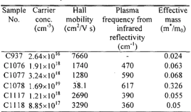
Fig.1 shows the DXRD rocking curves of InAs and InAsN samples. As plasma power increased, the diffraction peak of the InAsN, as compared with that of lnAs sample, shifts closer to the InP substrate peak. It represents that N was indeed incorporated into InAs. The results from RADS fitting were also summarized in the Table I . Although N was added into InAs successfully, its incorporation also degrades the DXRD linewidths as compared to the referential InAs. It suggests the existence of the residual strain or immiscibility introduced by the small diameter N atoms seated on arsenic sites. Table I shows the Hall results of the samples at room temperature. All the undoped samples exhibited n-type conduction. It was found that the more the N composition, the higher the carrier concentration. The possible origin of the high carrier concentration in N-containing sample is not quite clear at the moment. As compared with other N-containing samples, the sample C 1078 has the largest residual free carrier concentration and an extraordinary low mobility. According to anticrossing model (5), the dispersion relation of the nonparabolic subbands become flatter as the nitrogen
2.8
1.6
1.2
0.5
Table 2 Carrier concentration, Hall mobility, plasma frequency, and electron effective mass of the studied samples
Sample Carrier Hall Plasma Effective No. conc. mobility frequency from m:ss
( ~ m - ~ ) (cm2/V s) infrared (m /mo) c937 2 . 6 4 ~ C1076 1 . 9 1 ~ C1077 3 . 2 4 ~ Cl078 1 . 6 9 ~ Cl117 1.21x Cl118 8 . 8 5 ~ reflectivity (cm-') Oi6 7660 0.024 01* 1740 470 0.063
oi8
1280 590 0.068oi9
3'8.1 617 0.326 0" 2690 390 0.055 0'' 3290 360 0.05composition is increased. This indicates a large increase of the effective mass in the subbands. Furthermore, the higher residual free carrier concentration in sample C1078 may make the nonparabolic effect on the subband more significant, and therefore results in very low mobility. Fig2 shows the near band edge absorption spectra. The absorption coefficient a is converted from FTIR transmission measurement. Two points are worthy of note from this figure. First, the energy of the absorption edge of lnAsN samples is always higher than that of InAs. Second, when N composition is lower than 1.6%, higher N composition results in higher absorption edge. But, the trend reverses for InAsN with larger N composition. The phenomenon seems controversy to the theoretical prediction (I). To interpret the results, Burstein-Moss effect (6) should be taken into account because of the high carrier concentration in these InAsN samples. Samples with lower N composition have smaller effective mass and thus more
significant Burstein-Moss effects. The two high N content samples, however, have larger effective mass and thus their Burstein-Moss
l . 0 X l O 8
-
-
C1075- - -
C1076C1077
/.
I-..-
Fig. I DXRD spectra of a series InAsl-,N, bulk samples with x from 0 to 0.028.
0.3
Fig. 2 Plots of the square of the absorption coefficien
(a') against the photon energy deduced from 300
IR transmission spectra recorded on a series o InAsl.,N, bulk samples with x from 0 to 0.028
effects are less significant. In these two samples, C1078 (2.8%) and C1077 (1.6%), the bowing effect on band gap may have overcome the Burstein-Moss effect, and results in red-shifted absorption edge, though the carrier concentration of the former is five times higher than that of the latter.
To evaluate the energy shift caused by Burstein-Moss effect, we need the effective mass of electron. The method we used to determine the effective mass is IR reflectivity measurement. In a higher residual carrier concentration InAsN with a well-defined plasma edge up, the electron effective mass at the Fermi energy can be determined from
Ne2
0 - =-
"
m
E , E ~where e is the electron charge,
N
is the free electron concentration, is the high frequency dielectric constant (here we assume an of 12.25) and EO is the permittivity of free space. In Eq.[ I ] we neglect the tensor character of the effective mass. A typical reflectivity spectrum of InAsN sample is shown in Fig.3. As can be1.0 r 1 0 8 0 6 0 4 0 2 0 0 I InAs.
t
"%\
}
T=300K 300 400 500 600 700Fig. 3 A typical experiment reflectivity spectrum (solid line) for InAsN samples. The dashed line represents the fitting curve with indicated parameters using the methods described in Ref.(7).y is
a phenomenological damping rate.
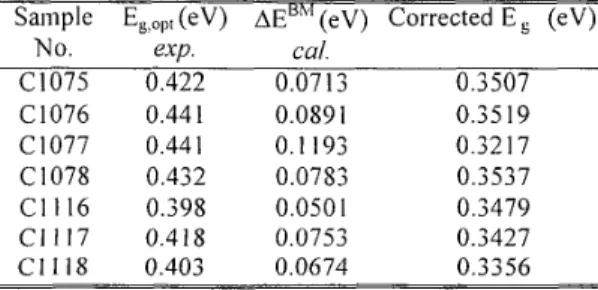
Table 3 Summary of the band gap energy of the InAsN samples and the energy shift caused by Burstein-Moss effect AEBM.
Sample (eV) AE"'' ( e v ) Corrected E (eV) C1075 0.422 0.0713 0.3507 C1076 0.441 0.089 1 0.35 I9 C1077 0.441 0.1 193 0.32 17 C1078 0.432 0.0783 0.3537 C l 116 0.398 0.0501 0.3479 CI 117 0.418 0.0753 0.3427 Cl118 0.403 0.0674 0.3356
No. exp. cui.
557
seen, the onset of the plasma reflection edge is at 470cm-'. The dashed line represents the fitting curve using the method described in Ref. (7). Taking plasma wavelength into Eq.[l] one can find the electron effective mass. The plasma frequency and the calculated electron effective mass of InAsN samples are summarized in Table 2. A very large increase of the effective mass is found in samples with higher N composition, which it is in good qualitative agreement with the predictions of the anticrossing model. The electron effective mass of the C1078 is extraordinary larger than other samples. This result supports the arguments we use to interpret the extraordinary low mobility for the same sample in previous Hall results. The energy shift caused by band filling effect can be calculate by taking Hall results and the effective mass derived from IR reflectivity data into the following equation:
where A is Planck's constant, in* is the conduction effective mass determined from IR reflectivity measurement, and N is the residual free carrier concentration determined from Hall results. The results are listed in Table 3. After subtracting the energy caused by Burstein-Moss effect from the absorption peak edge and neglecting the band gap narrowing term, the corrected band gap energy of each InAsN sample is obtained and the bowing effect reappears in these InAsN samples. Fig. 4 shows the composition dependence of the corrected band gap energy of InAsN. Besides our own results, previous published data by other research group (8) are also included. Two curves represent theoretical calculations based on dielectric model and tight binding method (9), respectively. In low N composition region, as can be seen in Fig. 4, our experimental results are close to the theoretical curve calculated from tight binding method.
IV.
Conclusions
InAsN alloys with various N compositions were successfully grown on InP substrate by using plasma-assisted GSMBE. When N composition increases, InAsN film has broader FWHM in DXRD spectrum and higher residual carrier concentration. Dramatic increase on the electron effective mass and decrease on the carrier mobility due to the N incorporation in InAsN alloy were observed. The absorption edge of InAsN alloy, as compared to that of InAs, shows blue-shift. After subtracting the energy caused by Burstein-Moss effect from the absorption peak edge, the bowing effect reappears in these InAsN samples.
0.05
t
\
‘ I “ ’ I ’ 1 ’ 0.a 0.01 0.Q 0.a 0.04 0.05 QC6 0.07
N”ti0n
Fig.4 Composition dependence of the band gap of InAsN. The points represent experimental data and two curves represent theoretical calculations.
Acknowledgements
This work was supported by the National Science Council and the Ministry of Education of the Republic of China under Contract No. NSC 89-2215-E-002 -034 and 89-N-FAO 1-2-4-3, in respectively.
Reference
( I ) S. Sakai, Y. Ueta, and Y. Terauchi, Jpn. J. Appl. Phys., “Band gap energy and band lineup of 111-V alloy semiconductors incorporating nitrogen and boron”, (2) Y. C. Kao, T. P. E. Broekaert, H. Y . Liu, S. Tang, I. H.
Ho, and G. B. Stringfellow, Muter. Res. Soc. Symp.
Proc., 423, 5 , 1996.
Schwartzman, “Microstructure and composition of InAsN alloys grown by plasma-source molecular beam epitaxy”, J.
Vuc. Sci. Technol. B , vol. 16, pp.1293-1296, 1998.
(4) J . W. Matthews, and A. E. Blakeslee, “Defects in epitaxial multilayers”, ./. Cryst. Growth,. vol. 27,
(5) W. Shan, W. Walukiewicz, J. W. Ager I l l , E. E. Haller, J. F. Geisz, D. J. Friedman, J . M. Olson, and S. R. Kurtz, Phys. Rev. Lett., “Band anticrossing in GaInAsN alloys”, vol. 82, pp.1221-1223, 1999. (6)E. Burstein, Phys. Rev., “Anomalous optical
absorption limit in InSb”, vol. 93, pp.632-633, 1954. vol. 32, pp.4413-4417, 1993.
(3) R. Beresford, K. S. Stevens, and A. F.
pp.118-125, 1974.
(7) P. Perlin, E. Litwin-Staszewska, B. Suchanek, W. Knap, J. Camassel, T. Suski, R. Piotrzkowski, I. Grzegory, S. Porowski, E. Kaminska, and J.C. Chervin,
Appl. Phys. Lett., “Determination of the effective mass
of GaN from infrared reflectivity and Hall effect”,vol. (8) H. Naoi,Y Naoi, and S. Sakai, Solid State Eleclron., “MOCVD growth of InAsN for infrared applications” ,41, 3 19, 1997.
(9) T. Yang, S. Nakajima, and S. Sakai, Jpn. J. Appl
Phys., “Tight binding calculation of electronic structures of InNAs ordered alloys”, 36, L320-L322,
1997
76, pp.2409-24 I I , 2000.