M01C-2
0 . 8 m m C M O S
A
0.6-22-GHz
Broadband
CMOS
Distributed Amplifier
Ren-Chieh Liu, Kuo-Liang
Deng
andHuei
WangDept. of Electrical Engineering and Graduate Institute of
Communication,
NationalTaiwan
University,Taipei,
Taiwan, Republic of Chinaroger@aic:ee.ntu.edu.tw
[51 Bondwire inductors 0.3 - 3 5
*
1.2 0 . 7 2 ~ 0.32 5.1 - 7 4.7 c -6 4 - 9 3 5 4Abstrncf
-
A CMOS distributed amplifier (DA) covering 0.6 to 22 GHz is presented in this paper. Cascode gain cells and m-derived matching sections are used to enhance the gain and bandwidth performance. The DA chip achieves measured gain of 7.3 f 0.8 dB with chip area of 0.9 x 1.5 mm’ including testing pads. The amplifier was fabricated in a standard 0.18-pm CMOS technology and demonstrated the highest frequency and bandwidth of operation among previously reported amplifiers using regular CMOS processes to date.I. INTRODUCTION
Broadband amplifiers find many applications such as instrumentation, electronic warfare and broadband optical communication. Distributed amplifiers (DAs) were widely used for realizing broadband amplifiers in GaAs hybrid and MMIC technologies [l-41. Recently, DAs in CMOS process were also reported because of the advantages of low cost and integration ability with baseband circuits [5-IO].
A DA using packaging and bond-wire inductors
was presented in a 0.8-pm CMOS process with 5 f 1.2-dB gain form 300 lcHz to 3 GHz
[SI.
Using the 0 . 6 y m CMOS process, a fully integrated DA using on-chip planar spiral inductors achieves a measured pass-band gain of 6.1 dB with 5.5-GHz unity-gain bandwidth [ 6 ] . On the other hand, a fully differentialDA achieves 5.5-dB pass-band gain and 8.5-GHz unity gain bandwidth [7]. Using a SOS n-MOSFET process to avoid the substrate loss, a DA with a bandwidth of 10 GHz and 5-dB gain was demonstrated in a 0.5-pm SOS NMOS process
[XI.
For DAs using 0.18-pm CMOS process, a three stage DA designed with coplanar strip lines demonstrated a low frequency gain of 5 dB, sloping down to 1 dB at15 GHz [9], and two DAs using high impedance coplanar waveguides as inductive elements demonstrated 8 and IO-dB gain up to I O GHz, respectively [IO]. The operating frequencies of the previously published DAs are all below than 10 GHz.
In this paper, we reported the first 0.6-22-GHz broadband CMOS DA using a standard 0.18-pm
Chip Area Unit Gain SI1 S22 VDD PDc
Chip Feature Gain (dB)
I
(mm’)I
N F (dB)I
Freq. (GHz)I
(dBL] (dB)I
(V)I
(mw)I
Bandwidth (GHz)
Process
Table. I . Recently reported performance of CMOS distributed amplifiers. SOS: Silicon-on-Sapphire. CPS: Coplanar
strip lines. CC: Cascode topology.
0-7803-7694-3/03/$17.00 0 2003 IEEE
103
CMOS technology. With cascode gain cells and m- derived matching sections, this DA achieves measured results of 7.3
*
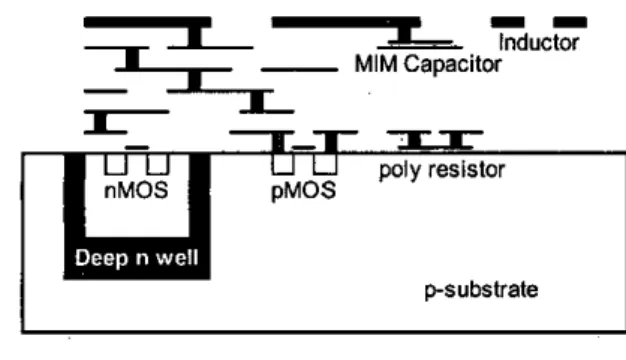
0.8 dB gain and input/output retum loss better than 8 dB from 0.6 to 22 GHz. Table 1 summarizes the recently reported performance of CMOS distributed amplifiers 'compared with this work. Our chip demonstrated the highest frequency and bandwidth of operation with good input and output retum loss.II.O.18pm CMOS TECHNOLOGY The D A chip was designed using a commercial 0.18-pm 1 P6M CMOS process, which provides single poly layer for the gates of the MOS and six metal layers for inter-connection as shown in Fig. 1 [ l l ] . The substrate conductivity is approximately
IO
S/m. Using optimized CMOS topology and deep n- well, this technology provides a f r of 60 GHz and
f i m of 55 GHz at 10 mA, a f r of 70 GHz andfMax of
58 GHz at maximum-transconductance bias, and a minimum noise figure of 1.5 dB without ground- shielded signal pad. High-Q inductors can be formed using the top AlCu metallization layer of 2-pm thickness without added mask. A MIM capacitor of 1 fF/mm2 has been developed using oxide inter-metal dielectric. Two types of polysilicon resistors, with several WO and k W o , are provided by choosing the individual dose of ion-implantation separately form the gate electrode doping process.
I
--
;ucrz
T
~-
MIM Capacitor poly resistorpsubslrate
Fig. 1 . The cross-section ofthe commercial 0.18-pm 1P6M
CMOS process
111. CASCODE CONFIGURATION
The cascode configuration, known for its high maximum available gain, wide bandwidth, improved
104
input-output isolation, and variable gain control capability, have been utilized in may applications such as mixers, frequency multipliers and distributed amplifiers.
The maximum available gain of the FET device is strongly affected by the feedback capacitance and output conductance [12]. FETs in cascode configuration show a reduction of feedback capacitance and output conductance compared to standard FETs, so the power gain of a cascode pair is considerably higher than that of a common-source FETs. Fig. 2 compares the maximum available gain and maximum stable gain of.cascode and common- source stages for the NMOSs with a total gate-width of 160 pm, based on the S-parameters of a common- source NMOS from 1 to 30 GHz.
.. 20 .. e... . . -. .
-
..
..
10 . .. .. . . . 0 O L0
10 20 30 Frequency (GHz)Fig. 2. M a x i " available gain of a single transistor and cascode- connected transistors.
Conventional cascode FETs suffer from a large feedback capacitance, the drain-source capacitance of the common-gate transistor. This makes it tend to be unstable and thus more difficult to use in an amplifier circuit than a common-source FET. Since the stability is an important issue in an amplifier design, a small damping resister
R
,
is usually added in the gate of common-gate transistor to improve the amplifier stability.N.
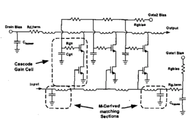
CIRCUIT DESIGN AND FABRICATION DAs are broadband circuits whose gain-bandwidth product substantially exceeds the transistor unit-gain frequency f ~ , because the input and output capacitances of the active devices are absorbed in the distributed stmctures. A conventional D A consists ofan input and an output transmission lines coupled by the transconducatnces of the MOSFETs. The transmission lines are formed by using lumped inductors as shown and are referred to as the gate and drain lines. The gate line is periodically loaded by the MOSFET gate-source capacitance and is terminated in its characteristic impedance at the end. As the RF signal travels on the gate line, each transistor is exited by the traveling voltage wave and transfers the signal to the drain line through its transconductance. If the phase velocities on the gate line and drain line are equal, then the signals on the drain line add in the forward direction as they arrive at the output. The out-of-phase wave traveling in the reverse direction will he absorbed by the drain-line termination.
The proposed CMOS DA was designed using cascode gain cells and m-derived matching sections, as shown in Fig. 3. The models of the capacitors and resistors were provided by the foundry. The S- parameters of the inductors were simulated by the EM simulator, Sonnet 6.0 1131. After layout optimization, the inductor gives the peak-Q of 12 at 1.9 GHz and 10 at 2.4 GHz for inductance of 1.5 nH and 4.lnH respectively. The MIM capacitor gives Q of 100 and 40 at 2.4 GHz and 5.3 GHz respectively at 1. I pF. The cascode devices employ a 1042 damping resistor. A die micrograph is shown in Fig. 4. The chip size is approximately 0.9 x 1.5 mm2 including testing pads.
V. MEASUREMENT RESULTS
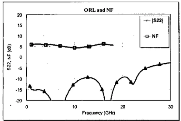
The CMOS DA was tested via on-wafer probing. Figs. 5 and 6 show the measured S-parameters and noise figure. The worst-case of the input retum loss has a value of 8 dB at 4 GHz, and is 10 dB or better from 0.6 to 22 GHz. The worst-case of the output retum loss has a value of 9 dB at 12 GHz and remains better than
IO
dB over most of the bandwidth. The reverse isolation is 20 dB or better over the entire bandwidth as well. The measured results agree with the simulated results very well. The noise figure is between 4.3 dB and 6.1 dB over 0.6 to 18 GHz. The circuit is not optimized for noise performance, but the noise figure of the circuit is still comparable with other previously published CMOS DAs.Fig. 3. Schematic circuit diagram of the cascode CMOS DA.
Fig. 4. Microphotograph of the CMOS DA.
VI. CONCLUSION
A fully integrated DA has been designed, fabricated and tested. This CMOS DA demonstrated 8-dB gain and 0.6-22-GHz bandwidth, which is the highest frequency and widest bandwidth of operation reported to date for broadband CMOS 'amplifiers. Since this DA was fabricated using a commercial 0.18ym CMOS technology, it can be easily integrated with other front-end circuits to build CMOS transceivers without requiring any post- processing steps.
Fig. 5. Measured power gain S 2 , and input retum loss S I ,
Fig. 6. Measwed noise figure NF and output retum loss Szz
ACKNOWLEDGEMENT
This work is supported in part by National Science Council (NSC 89-2213-E-002-178 and NSC 90- 22 19-E-002-007) and Research Excellence Program funded by Department of Education of Republic of China (ME-89-E-FA06-2-4-6). The chip is fabricated by TSMC through the Chip Implementation Center (CIC), Taiwan, ROC. The authors would like to thank Kun-You Lin, Chi-Hsueh Wang and National Nano-Device Laboratory (NDL), Taiwan, ROC, for the chip testing.
REFERENCES
[I] J. B. Beyer, S . N. Prasad, R. C. Becker, I. E. Nordman and
G. K Hohenwalter, “MESFET distributed amplifier design guidelines,” IEEE Tran. on M7T, vol. 32, no. 3, pp. 248- 275, Mar. 1984
[2] K. W. Kobayashi, 1. Cowles, L. T. Tran, T. R. Block, A. K.
Oki and D. C. Streit, “A 2-SO-GHz InAIAsilnGaAs-InP HBT Distributed Anmlifier.”
.
.
IEEE GaAs IC Svmo. _ . Die.. I... DD.207-210, 1996
131 B. Aearwal. A. E. Schrmtz. I. I. Brown. M. Matloubian. M.
L~ , ” ,
G. Case, M. Le, M. Lui, a d M. J. W. Rodwell, “1 12-dHz, 157-GHz, and 180-GHz In€‘ HEMT traveling-wave amolifiers.” IEEE Tran. on MlT, vol. 46. no. 12, DD. 2553- ..
2559, Dec. 1998
141 P. I. Sullivan. B. A. Xavier. and W. H. Ku. “A GaAs
L 1
MHEMT distributed amplifier with 300-GHz gain- bandwidth product for 40-Gbis optical applications,” IEEE MTT-SDip, pp. 1061-1064,2002
[ 5 ] P. I. SuUiiani B. A. Xavier, and W. H. Ku, “An integrated CMOS distributed amplifier using packaging inductance,” IEEE Tmn. on MTT, vol. 45, no. 10, pp. 1969-1975, Oct. 1997
[6] B. M. Ballweber, R. Gupta, and D. J. Allstot, “A hlly integrated 0.5-5.5-GHz CMOS distributed amplifier”, IEEE
J. Solid-State Circuits, vol. 35, no. 2, pp. 231-239, Feb. 2000
[7] H. Ahn. D. J. Allstot, “A 0.5-8.5-GHz fully differential CMOS distributed amplifier”, IEEE J Solid-State Circuits,
vol. 37, no. 8, pp. 985-993, Aug. 2002
[8] P. F Chen, R. A. Johnson, M. Wetzel, P. R. de la Houssaye,
G. A. Garcia, P. M. Asbeck, and 1. Lagnado, “Silicon-on- Sapphire MOSFET Distributed Amplifier with Coplanar Waveguide Matching,” IEEE RFIC98 Dig. Tech. Papers, pp. 161-164, 1998
[9] B. Kleveland, C. H. Diaz, D. Vook, L. Madden, T. H. Lee, and S . Wong, ”Monolithic CMOS distributed amplifier and oscillator,” IEEE ISSCC99 Dig. Tech. Papers, pp. 70-71, 1999
[IO] B. M. Frank, A. P. Frcundorfer, and Y. M. M. Antar, “ P e r f o r m ” of I-10-GHz Traveling Wave Amplifiers in
0.18-pm CMOS”, IEEE LMWC, vol. 12, no. 9, pp. 327-329, Sep. 2002
[ I I] H-M Hsu, I-Y Chang, I-G Su, C-C Tsai, S-C Wong, C. W. Chen, K. R. Peng, S . P. Ma, C. H. Chen, T. H. Yeh, C. H. Lin, Y . C. Sun, and C. Y. Chang, “A 0.18-p’m foundry RF CMOS technology with 70-GHz A for single chip system solutions,” IEEE MlT-SDigest, pp. 1869-1872,2001 [I21 M. Schlechtweg, et al., “Coplanar millheter-wave ICs for
W-band applications using 0.15pm pseudomorphic MODFET’s,” IEEE J, Solid-State Circuits, vol. 31, no. IO,
pp. 1426-1434, Aug. 1996, [I 31 http://www.soMetusa.com