Pergamon
Solid-Slate Electronics Vol. 38, No. 10, pp. 176Sl770, 1995 Copyright 0 1995 Elsevier Science Ltd Printed in Great Britain. All rights reserved
0038-I lOI/ $9.50+ 0.00
RELATION
BETWEEN THE COLLECTOR
CURRENT
AND
THE TWO-DIMENSIONAL
ELECTRON
GAS STORED IN
THE BASE-COLLECTOR
HETEROJUNCTION
NOTCH
OF InAlAs/InGaAs/InAlGaAs
DHBTs
CHAO-HSING HUANG, TSUEN-LIN LEE and HAO-HSIUNG LINT
Room 419, Department of Electrical Engineering, National Taiwan University, Taipei, Taiwan, R.O. China
(Received 18 November 1994; in revised form 20 December 1994)
Abstract-From the Gummel plots of InAlAs/InGaAs/I~,,,Al,G~,,_.~As double heterojunction bipolar transistors (DHBTs), the relationship between the collector current and the density of the two-dimensional electron gas (2DEG) stored in the base-collector (B-C) heterojunction notch is found to be an exponential function which stems from the thermionic emission escaping process of the ZDEG.
1. INTRODUCTION
Two-dimensional electron gas (2DEG) stored in a heterojunction notch is always an interesting and important subject. The applications of this phenom- enon have included various important semiconductor devices. One of the most important examples is high electron mobility transistor (HEMT), which has en- tered into our daily life. In heterojunction bipolar transistor (HBT), an emerging counterpart of HEMT, 2DEG also plays an important role on some of their characteristics. HBT with 2DEG emitter has been demonstrated[1,2]. In this design, 2DEG charges stored in emitter-base junction notch was used to attain low offset voltage, high current gain and offer high frequency performance. In In- AlAs/InGaAs DHBT, it was found that an extra 2DEG stored in the B-C heterojunction notch may push up the potential spike (2DEG effect) and cause a soft-rising output characteristics, i.e. the reach- through effect[3].
In these HBT examples, the density of 2DEG is a crucial factor which is determined by the heterojunc- tion band offset, the magnitude and capture rate of the current passing through it, and the doping con- centration of the heterojunction. To understand the relationship between them is not only a step to design HBTs with abrupt heterojunction but also an inter- esting topic of carrier transport dynamics.
In this study, the relationship between the collec- tor current and the density of the 2DEG stored in the base-collector (B-C) heterojunction notch was extracted from the Gummel plots of InAlAs/InGaAs/I~,s,Al,Gao,48 _,As DHBTs under
tTo whom all correspondence should be addressed.
several B-C bias voltages. The result is an exponen- tial function. By considering the balance between the trapping and escaping process of the 2DEG, we found the thermionic emission escaping process is the reason of the exponential behavior. HBTs with differ- ent InAlGaAs collector, i.e. with different band offset, were also studied. Conduction band offset is found to be a main factor to control the escaping barrier.
2. EXPERIMENT
The epilayers of the devices were grown on (100) InP substrate by using solid source molecular beam epitaxy (MBE). The dopant for n-type and p-type layers are Si and Be, respectively. The layer structures are summarized in Table 1. Notice that, between the InAlGaAs collector and the p +-InGaAs base, there is a 300-A-thick undoped InGaAs spacer which is used to remove the reach-through effect. There are six devices being studied. They are R504, R505, R506, R507, R508 and R640. For devices R504-R508, the only difference between them is on the composition of their Iq.szAl*.Ga,,.4, _,As collector. Besides, R640 has an InAlAs collector and a different base doping concentration. The In,,,,Al,G~,~,_.XAs collector composition, designed base doping concentration, and measured collector doping concentration are summarized in Table 2. The estimated collector band gap and base-collector conduction band offset of each device is also attached. The collector doping concentrations were measured from C-V method. To fabricate the DHBTs, an Au-G+Ni alloy was firstly deposited and lifted-off on the cap layer for the emitter ohmic contact. Solution 1 H,PO,: 1 H,Oz: 20 H,O was then used to remove both the cap and the
1166 Chao-Hsing Huang ef al.
Table 1, The layer structures of InAIAs/InGaAs/l~,,,AI,Ga,,,_ ,As DHBTs
Layer Material Thickness (pm) Doping (cm-‘)
Cap I IllAS 0.015 3 x 10’9
Cap 2 InGaAs 0.1 3 x 10’9
Cap 3 InAlAs 0.05 3 x 10’9
Emitter InAlAs 0.15 I x 10”
SpaC3 InGaAs 0.03 undoped
Base InGaAs 0.15 -
Spacer InGaAs 0.03 undoped
Collector InO.,,AI,GaO.,s- .As 0.4 -1 x 10’6
Buffer InGaAs 0.2 3 x 10’9
Substrate InP 350 I x lO’8(n)
Table 2. The parameters of base and In,,,AI,G%,,, _ ,As collector
Run No. R508 R507 R506 R505 R504 R640 Material (X) 0.00 0.12 0.24 0.36 0.48 0.48 E,(eV) A&(eV) 0.75 0.00 0.93 0.14 1.10 0.27 1.28 0.40 I .45 0.53 I .45 0.53 Doping (cm-‘) Base Collector 5 x lo’* 5.9 x 10’6 5 x 10’8 6.6 x lOI 5 x 10’8 6.8 x 10’6 5 x 10’8 6.6 x 10’6 5 x 10’8 6.3 x lOI 1.3 x lOI 5.8 x 10’6 25 I,=lOWstep I
Collector to emitter voltage, VcE (V)
(b)
257
Ig= 5pA/step0
0 1 2 3 4 5 6 0 1 2 3 4 5 6
Collector to emitter voltage, VCE (v) Collector to emitter voltage, Vc~ (VI
Fig. I. The common emitter output characteristics of DHBT: (a) R506; (b) R505; and (c) R504, respectively. The B-C conduction band offset of DHBT R506, R505 and R504 are 0.27, 0.4 and 0.53 eV,
Relation between 1, and 2DEG DHBTs 1767
emitter layer to expose the base layer. The followed Au/Ti nonalloyed contact was then deposited and lifted-off on the base layer. Finally, the devices were isolated by mesa etching in a 1 H,PO,: 1 H,O,: 20 H,O solution. The emitter area of the device is 60 x 60 pm’.
3. RESULTS AND DISCUSSIONS
Figure l(a), (b) and (c) show the common emitter output characteristics of DHBT R506, R505 and RS04, respectively. As summarized in Table 2, their B-Cconduction band offset are 0.27,0.4 and 0.53 eV, respectively. In Fig. l(a), the large 0.37 V offset voltage is due to the existence of E-B potential spike[4] which is preserved for hot electron launching. The sharp turn on collector current as can be seen in the saturation region indicates no reach-through effect in this device. In Fig. l(b), the collector current of the device, R505, shows a soft turn on in its saturation region. Reach-through effect can he clearly identified. In Fig. l(c), the device, R504, shows similar characteristics as R505. From the above results, it provides an important evidence for the band offset dependent 2DEG effect, which will be discussed later.
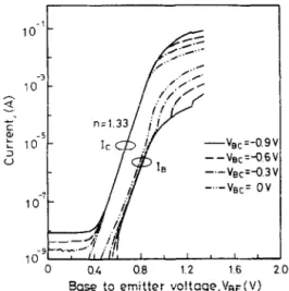
The Gummel plots of R505 with several different
B-C junction reverse bias voltages (Vet) are shown
in Fig. 2. As can be seen, in low current region, VK has no effect on the collector current. But, in high current region, the collector current splits into several branches. The more negative the reverse bias voltage, V,,, the higher the collector current. This finding provides an important evidence for the current- dependent 2DEG effect. According to our calculation based on depletion approximation in which the 2DEG charge is not considered, when V,, is smaller than -0.2 V, 300~A-thick InGaAs narrow band gap spacer is thick enough to pull down the heterojunc- tion spike and eliminate the reach through effect.
,0-l- /= .,:=..- .’ ..’ 1
o-3
-
,.A; ;‘,“//5
:
//
///
F n=1.33 E ; ,oc-:J,,,
k ;’ -v,,=-o.sv u ; 16 --v~~=-Osv --vfj~=-0.3v 16’ / -.-vBc= ov / / ,-,_-/ff ;‘j J-’ I I” 0 04 0.8 1.2 16 20Base to emitter voltage,VsE(V)
Fin. 2. The Gummel plot of DHBT R505 under different BzC junction reverse dias voltages (V,). T’he E-C conduc-
tion band offset of DHBT R505 is 0.4eV.
Base Spacer Collector
/
/ I
I
i---WC ---
Fig. 3. The B-C junction band diagram of DHBT under the turning point condition.
Therefore, in the low current region with V,, smaller than -0.2V, the collector current and the base current are independent of the reverse B-C bias voltage. When Vet is zero volts, our calculation indicates that the tip of the spike is 65meV higher than the conduction band minimum of the neutral base. This high spike begins to reflect injection car- riers back to the base region and enhances the base recombination current as can be seen in Fig. 2. In this low current region, because the increase of 2DEG charge in E-B heterojunction due to the carrier reflection is still not comparable with the ion charges of the E-B depletion region, the spike energy of E-B
heterojunction does not change. Since the collector current is controlled by the highest energy barrier it sees, i.e. the spike energy of E-B heterojunction[5,6], the collector current is not different from those with
V,, smaller than -0.2V. However, in high current region, care must be taken on the 2DEG charges, because their densities are comparable with the impu- rity ion charges. The collector current passing through the B-C heterojunction notch may provide enough 2DEG charge to push up the spike and cause the 2DEG effect. When the spike is high enough to reflect the injection carriers, the minority carrier concentration in the base as well as the 2DEG density in the E-B heterojunction notch increase. The former causes a sharp rising on the corresponding base current as shown in Fig. 2. The latter will push up the
E-B heterojunction spike, which will result in the decrease of the collector current. Furthermore, for the case of larger reverse B-C bias voltage, it needs more 2DEG density to push up the B-C heterojunc- tion spike to a certain level. Therefore, the decrease of the corresponding collector current takes place in higher current level.
Tiwari has presented similar Gummel plots[7], which were obtained from AlGaAs/GaAs DHBT
‘O’i
order to simplify the calculation, the 2DEG is as- sumed to be a delta function located on the hetero- junction interface, and depletion approximation is I. lm
used to find the electric field in the depletion region.*e . The first step of the procedure is to select a possible
r4
voltage drop across the depletion region of InAlGaAsA@
A4 side, Vc. Once the voltage drop is determined, the
maximum electric field of the depletion region, cmax, can be found by using depletion approximation. In
n R505(~Ec:O4eV)
al =
s
lo2
I
turn, the effective barrier height lowering, A4, can be
l R504(AEc=053eV) found by using TFE model. And the voltage drop
M640(AEc=053eV) across the depletion region of the InGaAs side, Vs,
is:
10'
1
’ 10 2x10" 4x10" 6x10"
n, (cmV2)
va =
7 _
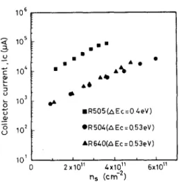
&#,,Fig. 4. The collector currents, 1,s as functions of 2DEG
densities, n,s. Circles, rectangles and triangles represent the where AE, is the conduction band offset, and q is unit data of DHBT R504, R505 and R640, respectively. charge. And the reverse bias voltage, Vet, is:
vBc= -(VB+ vc- Vbi) (2)
with graded base-collector junction. In his finding, where Vbi is the built-in potential of the junction. In the mobile charge from high collector current may the calculation, the possible Vc is readjusted to meet push up the heterojunction spike and cause the the required Vsc. Once VB and Vc are determined, soft-rising output characteristics. In our device, the charge densities of InGaAs side and InAlGaAs side, 2DEG effect appears at a current density as low as i.e. Q, and Qc, can be easily found, and the 2DEG 2%280A/cm2. At such low current density, the mo- sheet density can be estimated from the equation: bile charge is much lower than the impurity charges
and the 2DEG charge in the depletion region.
ns2L%!_
Therefore, the mobile charge effect and Kirk effect[8] 4
are not considered in this study. Figure 4 shows the collector current versus 2DEG As the Gummel plots shown in Fig. 2, each current density plots of devices R504, R505 and R640. The can be clearly divided into two parts on which the most striking result from this figure is that the B-C heterojunction spike does and does not cause the relationships between the collector current and the reach-through effect, respectively. The turning point 2DEG density of these devices follow exponential of each current corresponds to a similar band struc- law. In addition, the plots suggest that the smaller the ture as shown in Fig. 3. In this diagram, thermionic AEc, the larger the collector current for a given n,. field emission (TFE) model[9] is considered, and the These findings can be explained as follows. Figure 5 spike tip is higher than the conduction band mini- shows the schematic band diagram of the B-C het- mum of the base neutral region. The difference, Ad, erojunction notch. As shown in the figure, the supply- is just the effective barrier height lowering of the ing source of the 2DEG is the trapping of the model. Although the spike tip is higher than the collector current. And the trapping current, I,, is: conduction band minimum of the base neutral region,
the high tunneling rate due to the strong field around
the spike tip prevents the reflection of the injection where y is the trapping efficiency. The loss of the carriers. This effective barrier height lowering is 2DEG includes the recombination and thermionic relative to the electric field of the InAlGaAs side of
the B-C heterojunction and can be calculated from Base SDacer Collector
TFE model. The effect of Vet on the band structure is mainly on the depletion width of the InAlGaAs side
and the effective barrier height lowering. The latter is Ic
just slightly, therefore, the voltage drops across the
InGaAs base and spacer for different Vet are nearly EC the same. Since the band structures on the turning
points can be calculated, the collector currents and bias voltages VW s of these turning points provide us
an opportunity to study the relationship between the ---
current passing through a heterojunction notch and
’
ECthe 2DEG density stored in it.
The procedure used to calculate the 2DEG sheet Fig. 5. The schematic band diagram shows the supplying charges densitv. n.. is described brieflv as follows. In
current, escaping current, and emission barrier height of the
*. _I r 2DEG stored in a InAlGaAs/InGaAs heterojunction notch.
Relation between I, and 2DEG DHBTs 1769
emission of the ZDEG. The former can be neglected because of its magnitude, and the emission current, i.e. escaping current, Z,, should be proportional to
. .
the barner hetght, &,,,, seen by the 2DEG. As shown in the figure, the barrier height is:
448, = & - & = AZ% - qA4 - (& - E,) - J%, (5) where Ec is the conduction band minimum of the neutral base region, E, is the quasi Fermi level of the 2DEG, and E. is the ground state of the heterojunc- tion notch. And the escaping current of the 2DEG is:
1 a exp(-q&JW9 (6)
where k is Boltzmann’s constant and T is the absolute temperature. In steady state, the supplying rate should be equal to the emission rate, i.e. Zr = Z,. And the collector current can be expressed as:
z
C a
w(-q&M’7
Y (7)
If y is nearly a constant, then Zc is an exponential function of the emission barrier height, 4an.
According to eqn (S), & has four items. The first item, AE,, is determined by the material compo- sitions. The second item, A& can be found by using TFE model. The third item, (Ef, - E,), is relative to the 2DEG density, n,, and can be solved from the following equation:
dE
(8)
where h is the reduced Planck’s contant. The final item, E,,, is a function of cman, and can be found from the well known solutions of Airy functions for triangular quantum well[ 10);
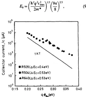
m f605(AEc=o.beV) l l?504(AEc=O.S3eV) Af?6dO(AEc=O.%+eV) loo - 015 0.20 0.2 5 0.30 0.35 0.40 4 +&lceV)
Fig. 6. The collector current 1,s as functions of the emission barrier height q&s. Circles, rectangles and triangles represent the data of DHBT R504, R505 and R640,
respectively.
where m * is the electron effective mass. Since t,, and n, are known, the emission barrier height, &, can be calculated. In our calculation, for the sake of simplifi- cation, only the ground state of the quantum well is considered.
Figure 6 shows the collector current, Zc, as a function of emission barrier height, &. Data from devices with different AE, are plotted in the figure. Again, the relation is an exponential function. How- ever, the most important is that the slope of the data is nearly NT. These results prove that the 2DEG supply current Zc is controlled by the thermionic emission process.
Based on this finding, it is very clearly that A& plays a very important role in the 2DEG effect. The 2DEG in devices with smaller AEc has smaller emis- sion barrier height, and needs higher supply current Zc to sustain a certain 2DEG density. This explains why our devices with AEc lower than 0.4eV do not have the reach-through effect. The reason is that their &,n~ are too small to prevent the escaping of 2DEG in normal operation current range. However, when the devices are driven to very high I,, the effect may reappear.
There is one interesting point in Fig. 6. As can be seen, for the same &, the collector current of device R505 is smaller than those of device R504 and R640. A possible reason is that the electric field applied on the depletion region of the InGaAs side under the turning point condition is relative to the conduction band offset. For device R505, its band offset is 0.4 eV, and the electric field is smaller than that of device R504 and device R640. The carriers in device R505 need longer time to pass through its InGaAs de- pletion region. Therefore, the trapping efficiency is higher. According to eqn (7) the collector current should be smaller.
4. CONCLUSION
In this study, DHBTs with In,,,, Al, Ga0.48 - .s As collector are investigated. From the Gummel plots of the devices with the 2DEG effect, the relation be- tween the collector current and the 2DEG density is found to be an exponential function which is mainly resulted from the thermal emission escaping process of 2DEG charges. It is also found that the conduction band offset is a main factor to control the escaping barrier.
Acknowledgements-This study was partially supported by the National Science Council of the Republic of China under contract No. NSC-82-0404-EOO2-244 and the Telecommunication laboratory, Ministry of Communi- cation of the Republic of China under contract No. TL- NSC-82-5107.
REFERENCES
I. Q. Wang, Y. Wang, K. F. Longenbach, E. S. Yang and W. I. Wang, Appl. Phys. Len. 59, 2582 (1991).
770 Chao-Hsing Huang et al.
2. Q. Wang, E. S. Yang, Y. K. Chen, D. Sivco and A. Y. 6. S. C. Lee and H. H. Lin, J. appl. Phys. 59, 1688 (1986). Cho, Appl. Phys. Lat. 62, 3129 (1993). 7. S. Tiwari, IEEE Electron Device Lett. 9, 142 (1988). 3. C. H. Huang and H. H. Lin, Solid-St. Electron. 36,1229 8. C. T. Kirk, IRE Trans. Electron Devices ED-3, 164
(1993). (1962).
4. S. C. Lee, J. N. Kau and H. H. Lin, Appl. Phys. L&t. 9. S. Tiwari, Compound Semiconductor Device Physics, 45, I1 14 (1984). p. 234. Academic Press, New York (1992).
5. C. Z. Chen and S. C. Lee, IEEE Trans. Electron Devices 10. S. Tiwari, Compound Semiconductor Device Physics,