國
立
交
通
大
學
電子工程學系 電子研究所碩士班
碩 士 論 文
N 型多晶矽薄膜電晶體元件製作與高頻特性分析
Fabrication and High-Frequency Characterization of
N-type Poly-Si Thin-Film Transistors
研 究 生: 林廷燿
指導教授: 林鴻志 博士
黃調元 博士
N 型多晶矽薄膜電晶體元件製作與高頻特性分析
Fabrication and High-Frequency Characterization of
N-type Poly-Si Thin-Film Transistors
研 究 生: 林廷燿
Student : Ting-Yao Lin
指導教授: 林鴻志 博士
Advisors: Dr. Horng-Chih Lin
黃調元 博士
Dr. Tiao-Yuan Huang
國 立 交 通 大 學
電子工程學系 電子研究所碩士班
碩 士 論 文
Submitted to Department of Electronics Engineering & Institute of Electronics College of Electrical Engineering and Computer Engineering
National Chiao Tung University in Partial Fulfillment of the Requirements
for the Degree of Master of Science
in
Electronics Engineering September 2012
Hsinchu, Taiwan, Republic of China
i
N 型多晶矽薄膜電晶體
元件製作與高頻特性分析
研究生:林廷燿 指導教授: 林鴻志 博士 黃調元 博士 國立交通大學 電子工程學系 電子研究所碩士班摘要
本篇論文中,吾人製作 N 型薄膜電晶體元件並研究其高頻特性。高頻特性 容易受到寄生效應的影響,因此降低寄生效應為特性好壞的主要關鍵。此薄膜電 晶體使用了矽化鎳來降低源極、汲極和閘極的接觸電阻,另外也利用了過度曝光 與光阻微調技術微縮了閘極的長度來改善高頻特性。我們還發現在多指型閘極結 構中,雙重微影成像技術容易造成閘極長度的誤差,使得在關閉狀態時電流會傾 向從較短的閘極長度處漏走。 此外,我們成功的藉由小訊號模型萃取出小訊號參數,由 S 參數比較模擬與 量測結果,證實了小訊號模型的正確性。與單一閘極結構的小訊號參數相比,我 們可以發現在多指型閘極結構中的寄生電阻會變小,寄生電容會增加,但整體來 說對改善截止頻率與最大震盪頻率還是有利的。雖然外部阻抗很大而且可能會影 響到實際的交流性能,但是由模擬結果證實是可信的。歸一化量測值與模擬結果 做比較,可明顯發現兩者趨勢是相符的。ii
Fabrication and High-Frequency
Characterization of N-type Poly-Si Thin-Film
Transistors
Student: Ting-Yao Lin Advisors: Dr. Horng-Chih Lin Dr. Tiao-Yuan Huang
Department of Electronics Engineering and Institute of Electronics National Chiao Tung University, Hsinchu, Taiwan
Abstract(English)
In this thesis, we have fabricated n-type poly-Si thin-film transistors (TFTs) and
studied their high frequency characteristics. High frequency characteristics are
affected easily by the parasitic components, hence reduction of these components is
essential. Resistances of source, drain, and gate are reduced with the aid of Ni
silicidation technique in this work. To effectively shrink the gate length, we used both
over-exposure and photoresist-trimming techniques to shrink the dimension of the PR
patterns. These actions are helpful in improving the high frequency characteristics.
However, we found the fluctuation in the dimensions of the interdigital poly-Si gate
iii
shortened gate lengths in the interdigital gate structures tend to increase the off-state
current.
We’ve also successfully extracted the small-signal parameters by using a
small-signal model. The simulation results of S parameters agree well with the
measured data, confirming the accuracy of the small-signal model. As compared with
the device with single-gate pattern, the values of parasitic resistances become smaller
and the values of parasitic capacitances increase in the interdigital gate structure. But
it is still beneficial for improving cut-off frequency and maximum oscillation
frequency with the interdigital gate structure. Although the extrinsic resistances are
large and may affect the practical ac performance, the analysis is confirmed with the
simulation results and proved to be reliable. From both the normalized data and the
comparison of the experimental results with the simulation, it is observed that the
iv
Acknowledgement
這個致謝我遲遲拖到了口試結束的今天才下筆,這是因為到了今天,碩士生 涯才算是完整的結束,我的文筆不好,或許沒有辦法完整傳達我所有的想法,卻 有著我最深的感動與不捨,這兩年來要感謝的人很多,絕對不能只謝天就好。 我最感謝的莫過於指導我碩士生涯的兩位指導教授 林鴻志 教授及 黃調元 教授,包容我在研究上的不成熟。林老師不只給我在論文上面的指導,給我正確 的研究方向,也常常提醒我,不管是現在身為研究生或是之後身為研究人員,在 做研究時面對困難應有的態度。黃老師除了在半導體領域上有著專業及寬廣的知 識,最讓我印象深刻的就是黃老師的深不見底的中文造詣和陽光般的笑容,看到 老師的笑容,彷彿心情都好了起來。 能夠完成此論文還要感謝口試委員楊文祿教授與陳坤明博士的指教,讓我更 清楚研究上的缺點以及疏失,對本論文有更深的了解,當然林老師和黃老師對於 此論文內容以及英文文法十分嚴謹,幫忙缺乏英文論文寫作經驗的我能夠交出一 份漂亮的碩士論文。 在 ADTL 這個實驗室,認識了很多人,不管是在研究上、生活上,都給我 莫大的幫助。蔡老大總是很用心的帶我做研究,不厭其煩的回答我一些蠢問題, 在製程上的經驗非常老到,幫我避開了很多會在製程上遇到的問題,省了很多時 間,雖然隨著我們越來越熟,你充滿色彩的笑話也常讓我無法接話,不過衷心覺 得有你真好,另外撇開幽默感不說,你真的是個蠻不錯的男人。阿民雖然早我們 一步畢業,無法陪我們到最後,但感謝你在模擬和電性上的指導,聽說你好像有 看好我,不過我好像讓你失望了。阿毛和馬腳總是在實驗室裡唱雙簧,見識到你 們獨特的幽默,也在我研究遇到困難時,給了我很多不同的想法與意見,也感謝 你們為了實驗室的大家切了很多 FIB,那真的是一個費神又費時的苦工,你們的 付出,大家都有目共睹。剛到實驗室時,發現嘉文學長是我大學同校的學長,讓 我有點受寵若驚而且額外親切,嘉文學長對於研究與英文的堅持,是我應該要去 學習的,另外嘉文學長的冷幽默也是一絕。克慧學姊也常給我一些在實驗與量測 上的意見,還有傳授一些小撇步。委屈阿莫常常跟這我們這屆小碩班一起瘋一起 鬧,不過也因為這樣我們的感情很 close 啦(自以為)!看著你常在開口第一句就說 好餓喔!好脹喔!也漸漸習以為常,但是實驗要做,身體也要顧啊!阿哲哥真的身藏 不露,除了桌球打得好外,有幸看到你帶學弟做實驗能在暑假就有成果,實在是 神人等級。管金儀學長,ADTL 是個不錯的實驗室,歡迎你加入,請好好享用。 再來要感謝的是一起打拼的各位好夥伴,一起做實驗,一起做研究,這滋味 是苦澀的,也是甘甜的。沒有人可以質疑交大電工所 101 級盈宇哥的帥氣,你可 以說是才貌兼備、智勇雙全,羨煞了我這個平凡人,很高興在六月底你陪我在實 驗室一起為畢業打拼,雖然你搶先我一步畢業,但那段回憶還是很不賴的。和乾 爹討論實驗,總是能讓我從另一個沒想過的角度去看實驗,有不一樣的思路,也 謝謝乾爹總是能不辭辛勞的開車帶我們出去玩,又要開車又要先研究路線,包住v 包交通實在是太令人感動了。乾媽一號彭彭無理頭的搞笑,為實驗室帶來了不少 歡笑,以及乾媽二號曉惠正妹常常帶好吃的給實驗室的大夥兒吃,兩位合體後的 hp 連線,行動力讓我很畏懼,砲火更是不同凡響,讓人無力招架。坐在乾媽三 號仙女姐姐旁邊兩年,都覺得我受到仙氣的影響,再加上你的鼓勵,讓我有了很 多做實驗的動力和正面的想法。 也感謝 ADTL 的學弟妹們,信宏、靜玲、維軒、婷婷、明鴻、佳文、浩君, 有了你們的加入,為實驗室帶來了不少歡笑,體諒我們因為做實驗完後有點死氣 沉沉。還有新加入 ADTL 的小學弟妹們,雖然跟你們沒講過幾句話,但就好好 享受這個大家庭吧!還有電工所 101 級的各位,我們的感情除了打屁聊天外,還 能跟大家討論功課和分享研究心得,外加運動吃飯出去玩樣樣不缺,真的很開心 可以認識大家。 還要感謝可說是朝夕相處的室友們,因為有他們,我可以在每天回到家後馬 上轉換心情跟室友打牌、聊八卦、喝酒,另外看到俊良每天過著壓力大兼閒置的 生活,讓每個人羨慕的要死。六年的室友小羊水果然不是當假的,總是在我研究 遇到困難的時後點醒我,把我拉出無限迴圈中。致緯、柏文的實驗室就在隔壁, 除了在家遇到外,去學校也有人罩,三不五時去 ED632 閒晃放鬆。還認識了庭 嘉,從學長變同事,好不習慣。在高頻研究上,我一定要感謝一個人,就是我大 學專題的戰友,現任中山大學 WSTL 的 GG 楷,要不是剛好被我抓到 GG 楷會用 ADS 模擬軟體,我真的不知道該怎麼樣在這部分有所突破,也委屈他不時的會 被我煩著追問問題,沒想到從大學開始要靠他的幫忙,到了研究所也是離不開 GG 楷,萬分感謝。感謝鴨鴨在這半年來的支持與鼓勵,給了我不放棄研究的動 力,忍受我因為太忙沒有時間陪。感謝大學的好朋友們,在我口試前緊張萬分時, 給了我一些鼓勵的話語及對付緊張的方法。 感謝家人無條件給我的支持與鼓勵,把我從小米蟲養到大米蟲,希望現在的 我有達到你們的期待。 謹以此論文獻給關心我、愛我的每個人。 林廷燿 謹誌於 交通大學 電子工程研究所 中華民國 101 年 9 月
vi
Contents
Abstract(Chinese) ... i Abstract(English) ...ii Acknowledgement ... iv Contents ... viFigure Captions ... viii
Table Captions... xi
Chapter 1 Introduction ... 1
1-1 Overview of Thin-Film Transistor Technology ... 1
1-2 Overview of Radio Frequency Techniques ... 3
1-3 Overview of Silicide Technology ... 5
1-4 Motivation ... 7
1-5 Organization of Thesis ... 8
Chapter 2 Device Fabrication and Measurements ... 9
2-1 Device structure and Process Flow ... 9
2-2 Measurement Setup ... 12
2-3 De-embedded Process... 13
Chapter 3 Results and Discussion ... 15
3-1 Basic Electrical Characteristics ... 15
3-2 Small-Signal Modeling ... 17
3-2-1 Modeling Setup Flowchart ... 17
3-2-2 Extrinsic Parameter Extraction... 17
3-2-3 Intrinsic Parameter Extraction ... 19
3-3 Experiment and Simulation Analyses ... 20
vii
4-1 Summary and Conclusion ... 27
4-2 Future Work ... 28
References ... 30
Figures ... 35
Vita ... 61
viii
Figure Captions
Chapter 2
Fig. 2.1 Process flow of the poly-Si TFT fabrication. ... 35 Fig. 2.2 In-line SEM image of patterned PR lines with Lmask of 0.25μm located at
different dies of a wafer before trimming. ... 36 Fig. 2.3 In-line SEM image of patterned PR lines with Lmask of 0.25μm located at
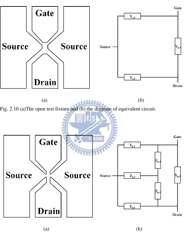
different dies of a wafer after trimming. ... 37 Fig. 2.4 In-line SEM image of patterned poly-Si lines located at different dies of a wafer after stripping off the trimmed PR. ... 38 Fig. 2.5 Cross-sectional TEM image of a n-type TFT device. ... 39 Fig. 2.6 The device design with interdigital gate structure. ... 39 Fig. 2.7 In-line SEM images of poly-Si gates patterned with (a) DR techniques with severe fluctuation and (b) SP techniques with greatly reduced fluctuation. .. 40 Fig. 2.8 Cumulative plots of measured dimensions of poly-Si gates patterned at different dies of a wafer with SP or DP methods with nominal gate length of 0.23μm. ... 41 Fig. 2.9 Equivalent circuit diagram used for the two-step correction including parasitic effect [2.2]. ... 41 Fig. 2.10 (a)The open test fixture and (b) the diagram of equivalent circuit. ... 42 Fig. 2.11 (a) The short test fixture and (b) the diagram of equivalent circuit. ... 42
Chapter3
Fig. 3.1 (a) Transfer and (b) output characteristics of n-type TFT with L/W = 0.2μm/8μm. ... 43 Fig. 3.2 (a) Transfer and (b) output characteristics of an SP n-type TFT with L/W = 0.2μm/64μm. ... 44 Fig. 3.3 Transfer characteristics of n-type TFTs at Vd = 0.1V patterned with SP and DP
ix
respectively. ... 45 Fig. 3.4 The flowchart of small-signal model setup. ... 46 Fig. 3.5 Small-signal equivalent circuit of an n-type TFT. ... 46 Fig. 3.6 (a) Cross-sectional view of n-type TFTs with a partially depleted channel under the zero condition and (b) the equivalent circuit model. ... 47 Fig.3.7 Method of extracting intrinsic Y-parameter matrix of the device. ... 48 Fig. 3.8 Intrinsic part of an n-type TFT. ... 49 Fig. 3.9 The cross section of an n-type TFT with corresponding small-signal equivalent circuit. ... 49 Fig. 3.10 Modeling results for extrinsic resistance extraction considering the neutral-body effect at cut-off condition for a device with channel thickness of 1000Å . (lines: Vd = 0V and Vg = -1V. symbols: Vd = Vg = 0V) ... 50
Fig. 3.11 Modeling results for extrinsic resistance extraction considering the neutral-body effect at cut-off condition for a device with channel thickness of 500Å ... 50 Fig. 3.12 Modeling results for Im(Y11+Y12), -Im(Y12), and Im(Y22+Y12) for a device
with channel thickness of 500Å . ... 51 Fig. 3.13 Modeling results for gm, and ro for a device with channel thickness of 500Å .
... 51 Fig. 3.14 Modeling results for τ for a device with channel thickness of 500Å . ... 52 Fig. 3.15 Measured results of ft and fmax for a device with channel thickness of 500Å .
... 52 Fig. 3.16 Modeling results of (a) S11 and S22 and (b) S12 and S21 at Vd = 2V and Vg = 4V.
(lines for measurements, symbols for models, channel thickness = 500Å ,and L/W = 0.22μm/8μm) ... 53 Fig. 3.17 Modeling results for extrinsic resistance extraction considering the neutral-body effect at cut-off condition for a device with channel thickness = 1000Å ... 54 Fig. 3.18 Modeling results of Im(Y11+Y12), -Im(Y12), and Im(Y22+Y12) for a device
x
Fig. 3.19 Modeling results of gm, and ro for a device with channel thickness = 1000Å
... 55 Fig. 3.20 Modeling results of τ for a device with channel thickness = 1000Å ... 55 Fig. 3.21 Measured results of ft and fmax for a device with channel thickness = 1000Å
... 56 Fig. 3.22 Modeling results of (a) S11 and S22 and (b) S12 and S21 at Vd = 2V and Vg = 2V.
(lines for measurements, symbols for models, channel = 1000Å ,and L/W = 0.22μm/8μm) ... 57 Fig. 3.23 ft measured at Vd = 1V and 2V for a device with channel thickness of 1000Å .
... 58 Fig. 3.24 Small-signal parameters extracted at Vd = 2V and various Vg for a device
with channel thickness of 1000Å . ... 59 Fig. 3.25 The ft and fmax measured at Vd = 2V and various Vg for a device with channel
thickness of 1000Å . ... 60 Fig. 3.26 Comparisons between analytical calculation (lines) and measured ft and fmax
(symbols) versus gate voltage for a device with channel thickness of 1000Å . ... 60
xi
Table Captions
Table 3.1 Summary of basic electrical characteristics of n-type TFTs with various channel thicknesses and widths. ... 25 Table. 3.2 Measured dimensions of poly-Si gates patterned with SP or DP method with nominal gate length of 0.22μm. ... 25 Table 3.3 Summary of the small-signal parameters of n-type poly-Si TFTs with various channel thickness and width. ... 26
1
Chapter 1
Introduction
1-1 Overview of Thin-Film Transistor Technology
Dr. Paul K. Weimer invented and contributed to the development of thin-film
transistors (TFTs) as he was employed at Radio Corporation of America in Princeton
in 1962 [1.1]. In this work cadmium sulfide was used as the active channel, while
source, drain, and gate were made of metals [1.1]. Since then several alternative
materials have been explored and used as the channel layer, such as hydrogenated amorphous silicon (α-Si:H) [1.2], and polycrystalline silicon (poly-Si) [1.3] [1.4].
The α-Si TFTs were developed much earlier than the poly-Si counterparts
because the α-Si:H material can be deposited on glass substrates at a low temperature
with plasma-enhanced chemical vapor deposition (PECVD). However, α-Si TFTs are
not feasible for high-performance circuits because of the low carrier mobility which is
typically less than 1cm2/V.s. Until Fa and Jew developed the first poly-Si TFT [1.2],
the demerits of α-Si TFTs were not appropriately addressed. Electron mobility of
2
processes are incompatible with the manufacturing of the liquid-crystal displays (LCD)
with low-cost glass substrates, hence, low-temperature polycrystalline silicon (LTPS)
techniques are developed. LTPS TFTs not only cost less, but also make the resolution
of active-matrix liquid-crystal displays (AMLCDs) higher [1.5]. However, the
occurrence of the kink effect may limit the application to analog circuits [1.6].
The grain size of poly-Si is one of the major factors influences the carrier
mobility. The effective mobility increases as the grain size is expanded. The grain size
of as-deposited poly-Si is smaller than that with the poly-Si re-crystallized from α-Si.
There are 3 popular methods for re-crystallization, including solid phase
crystallization (SPC), excimer laser crystallization (ELC) and metal-induced lateral
crystallization (MILC). However, properties of the re-crystallized materials are
strongly dependent on the technique employed and the conditions used in the process.
Firstly, the SPC process usually takes longer time, roughly 24-48 hours if processed
under 600℃. This requirement certainly affects the throughput and thermal budget.
Secondly, the ELC process takes much less time to fabricate, and the substrate does
not have to be subjected to high temperature environment. However, the surface of the
re-crystallized film is not smooth at all and protruding regions appear near the grain
boundaries [1.7]. Lastly, the MILC process which adds a little metal into α-Si is also
3
budget [1.8]. Usually poly-Si films produced with ELC or MILC schemes are with
much larger grains as compared with those produced with SPC.
Nowadays, LTPS TFT has the potential to become a widely applied technique for
related applications. For instance, AMLCD [1.6][1.9],
metal-oxide-nitride-oxide-polysilicon (MONOS) [1.10], and fingerprint scanning
array [1.11].
1-2 Overview of Radio Frequency Techniques
With the thriving in technology development, wireless transmission among
electronics gears doubtlessly prevails throughout our daily life. In early days the
transmission was mostly limited to the audio communication. Nowadays, accessing
data of other formats like texts or video images and a much larger capacity of data
transmission has been greatly demanded. Thus, speeding the speed of transmission is
a paramount issue to put focus on.
Over past decades, transistors have been widely used and continually developed
due to its mature technique. Moreover, operation frequency of the circuits
continuously improves thanks to the scaling down of devices. Many kinds of
4
divider, phase-locked loop (PLL), voltage-controlled oscillator (VCO), and low-noise
amplifier (LNA). Among them, the PLL is used for precisely controlling and
automatically modulating frequency [1.12]. VCO is another kind of oscillation
circuits which controls the oscillation frequency with voltage [1.13]. The purpose of a
LNA is to receive signal by antenna with high gain and sensitivity. In order to reduce
loss, LNA is usually put in the front of antenna [1.14].
Major factors for improving the electrical performance of transistors applied for
radio frequency (RF) circuits include high electron mobility, high transconductance,
high current drive, low parasitic resistance, low parasitic capacitance, and high
frequency response characteristics. By achieving those mentioned above, we could
improve cut-off frequency (ft) and maximum oscillation frequency (fmax). By properly
shrinking the dimensions of TFTs, the devices’ RF performance is expected to
improve significantly and becomes feasible for RF IC application. Additionally, the Si
TFTs fabricated on a flexible polymer substrate for construction of large-area RF
systems for applications in aerospace, such as phased array antennas for
communication, remote sensing, and surveillance [1.15]. The system-on-panel (SoP)
can be used to upgrade the displays and advance the function of many products. For
example, it could be integrated into a cell phone which is capable of doing transaction
5
1-3 Overview of Silicide Technology
The major metal silicides adopted today are developed from titanium (Ti), cobalt
(Co), and nickel (Ni), in that order. There materials offer a few advantages, such as
low resistivity, low contact resistance, good process compatibility, and can be formed
in a self-aligned manner. However, there also exist a few issues which have been
studied in numerous publications, like bridging, stress, thin film agglomeration, etc.
Ti-salicide was developed as the first salicide material. The early issue is the
severe bridging occurring over spacers due to lateral diffusion of Si atoms which react
with Ti on the spacers. The formed silicide forms conduction bridges connecting the
gate and source/drain regions. Applying a two-step annealing in N2 is capable of
overcoming the problem [1.17]. Specifically, the first step is performed at a relative
low temperature (650-700℃) to form C49 TiSi2 with higher resistivity. In this stage
bridging would not occur due to the low temperature. Then a wet etching is employed
to selectively remove the un-reacted Ti film on the wafer surface, including that on the
spacers. The second anneal is then done at a higher temperature ( > 800℃) to transfer
the C49 TiSi2 into C54 TiSi2 [1.18]. But the problem of a large thermal budget still
exists. Besides, the sheet resistance of silicide increases anomalously when the
devices are scaled down ( < 0.25μm). This phenomenon is called the
6
sub 0.25 micron-node.
Co-silicide succeeded Ti-silicide at 0.18um technology node and beyond. To
avoid bridging, a two-step anneal procedure is still used to form low-resistivity CoSi2
at a high temperature ( > 700℃) from high-resistivity CoSi of the first annealing done
below 500℃ [1.20]. Before the aforementioned process, a TiN capping layer is
usually deposited onto the Co layer and serves as a barrier to avoid oxidation during
the following annealing in N2, because Co-salicide process is sensitive to
contamination of the ambient, especially oxygen [1.21]. The major disadvantages of
Co-salicide are the narrow-line-width effect (occurring as line width smaller than
100nm) and a mass of Si consumption.
The Ni-salicide technology was proposed in 1991. The NiSi salicide for
0.4μm-CMOS exhibited nice characteristics [1.22]. The advantages of Ni-silicide
include less narrow-line-width effect, lower resistivity, lower contact resistance, lower
thermal budget, and less Si consumption [1.23][1.24]. Ni-salicide usually demands
only one step of anneal at a temperature ranging between 350℃ and 700℃ to form
low-resistivity NiSi. At such a temperature, Ni-salicide can be free from the bridging
issue. Besides, doping with 5% Pt-incorporation was found to increase the phase
transformation temperature [1.25]. From the application point of view, Ni-salicide
7
nodes owing to the fact that several properties mentioned above are superior to those
of Ti- and Co-salicide technologies.
1-4 Motivation
Displays have been widely-used in our daily life and it wouldn’t surprise us that
the hot products recently discussed and focused are the flat-panel types. Looking
inside them, TFTs are usually used as the switch of pixels in the AMLCDs. Besides,
the performance of TFTs has greatly improved in recent years and should be capable
of serving as the basic building blocks on ICs manufactured on the panel of displays.
For SoP purpose, ICs of different functions, like central processing unit (CPU),
memory, and RF, are demanded to be integrated on the same panel. Nonetheless, few
works are reported on studying the RF characteristics of poly-Si TFTs, owing to their
relatively low mobility as compared with the bulk Si counterparts, as well as the
rather large device size in modern manufacturing (e.g., channel length > 3μm).
However, considering the low-temperature processing and the capability of being
manufactured on glass or flexible substrates, this subject is worthy of exploration.
Several ways can be adopted to improve the RF performance of poly-Si TFTs. One is
to scale down the channel length which can readily increase the on current and the
8
work. In this work we adopt these approaches in the device fabrication and study the
RF characteristics of the fabricated devices.
1-5 Organization of Thesis
In Chapter 2, the process for an n-type poly-Si TFT is described and evaluated.
Utilization of photoresist-trimming techniques for device fabrication is stated. The
characterization scheme and measurement setup are also introduced
In Chapter 3, the experimental results on characterizing the fabricated devices,
including the transfer and output current-voltage (I-V), small-signal parameters
9
Chapter 2
Device Fabrication and Measurements
2-1 Device structure and Process Flow
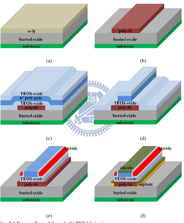
The process scheme is shown in Fig. 2.1. First of all, a wet oxide with thickness
of 1000 nm was formed on a six-inch silicon substrate as the buried oxide. An amorphous silicon (α-Si) layer was then deposited with low pressure chemical vapor deposition (LPCVD) to serve as the channel layer as shown in Fig. 2.1 (a). The
channel thickness was either 50 or 100nm. Solid phase crystallization (SPC) method,
which was performed at 600℃ in N2 ambient for 24 hours, was then used to transform
the film from α-Si into poly-Si in order to promote the electron mobility. The poly-Si layer was then defined to form active regions by an I-line lithographic and subsequent
anisotropic etching steps, as depicted in Fig. 2.1 (b). LPCVD tetraethylorthosilicate
(TEOS) oxide with thickness of 10nm was deposited as the gate oxide. Next, a 100nm
in-situ phosphorus doped poly-Si was deposited by LPCVD. Subsequently a 25nm
TEOS oxide was deposited to serve as the hard mask material by LPCVD as shown in
Fig. 2.1 (c). Afterwards, the gate was defined by a photolithographic step and etched
10
a 15nm nitride layer were deposited, and then etched by RIE for forming sidewall
spacers as shown in Fig. 2.1 (e). A 15nm-thick nickel layer was deposited and then
thermally processed at 450℃ by rapid thermal anneal (RTA) in N2 ambient to form
Ni-silicide on source, drain, and gate regions. Afterwards source/drain regions were
doped by a self-aligned implant with P31+ ions with energy of 10keV and dose of
5×1015cm-2 as shown in Fig. 2.1 (f). A 500nm-thick PECVD oxide layer was
deposited to act as the passivation layer in order to prevent the penetration of
humidity and impurity. Finally, a metallization process was performed to form metal
pads.
To effectively shrink the gate length, we used over exposure and
photoresist-trimming techniques to scale down the dimension of the PR patterns. The
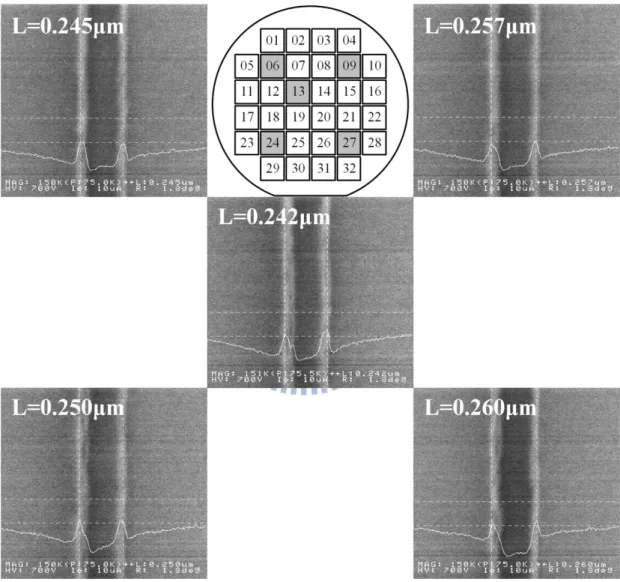
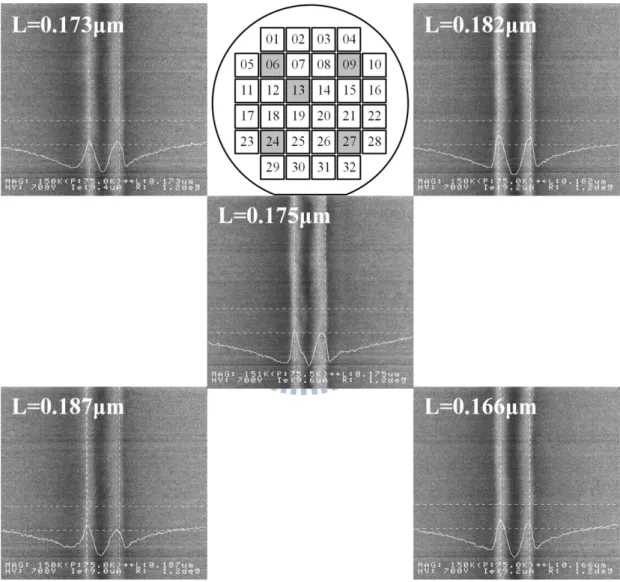
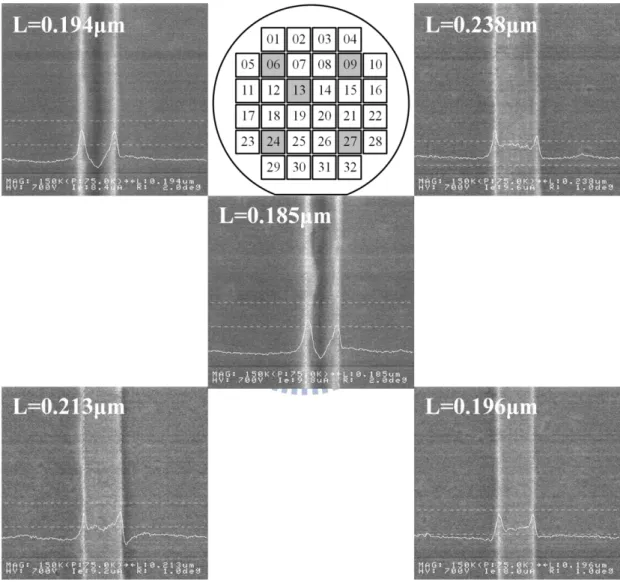
difference of patterned PR lines with Lmask of 0.25μm located at different dies
distributed on a wafer before and after trimming was inspected with the In-line
scanning electron microscope (SEM) and the results are shown in Figs. 2.2 and 2.3,
respectively. In this thesis, Lmask is the designed length of the structures on the mask,
and Lgate is the practical value measured with an In-line SEM. The results of poly-Si
line patterns with trimmed PR with Lmask of 0.25μm measured from five dies at
different location of a wafer are shown in Fig. 2.4. The measured Lgate ranges from
11
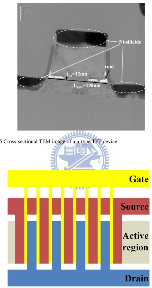
But the trimming method was found to have feet of clay, and the trimmed PR
would collapse when Lgate is further shortened. In this work we thus focus on devices
with channel length equals to or larger than 0.2μm. Cross-sectional transmission electron microscopy (TEM) image of a n-type TFT is shown in Fig. 2.5. The
unexpected voids seen in the picture were formed during the preparation of the TEM
sample by focus ion beam.
In order to promote ft, we hope hope that the fabricated devices provide high
transconductance. The feasible methods to increase transconductance include the
decrease in gate length, increase in gate width, and implementation of self-aligned
silicidation procedure to reduce the parasitic resistance. Interdigital gate-finger design
shown in Fig. 2.6 is adopted to avoid the current crowding phenomenon in the device.
In this work, in addition to the single patterning (SP) method mentioned above to
form the poly-Si gates, an additional split of samples with the poly-Si gates patterned
with a double patterning (DP) technique [2.1] was also fabricated and characterized.
However, because of the issues resulted from the overlay capability of the I-line
stepper and the dimension control of patterns during the manufacturing of the two
reticles used for the DP process, severe fluctuation in the dimensions of the final
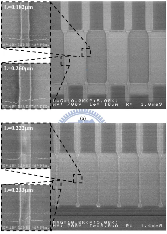
poly-Si gate patterns in the interdigital gate structures is observed. In-line SEM
12
shown in Figs. 2.7 (a) and (b). Severe gate pattern fluctuation can be identified in Fig.
2.7 (a), while the situation shown in Fig. 2.7 (b) is much better. The cumulative data
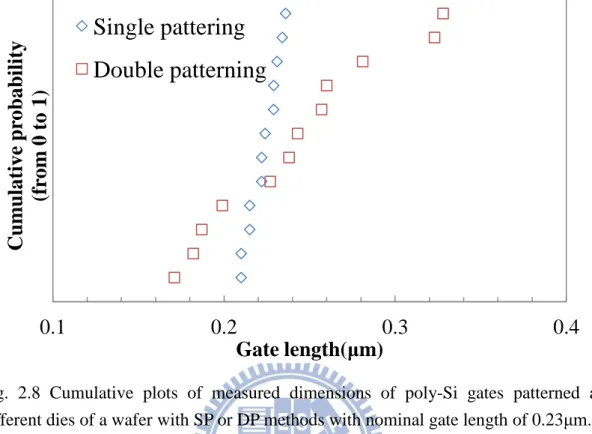
of the measured Lgate extracted from the two splits of devices with nominal gate length
of 0.22μm are shown in Fig. 2.8. In this picture, the measured data range from 0.21 to
0.238μm for the SP split, while the distribution for the DP split is widened from 0.171
to 0.328μm. The different outcome would draw impacts on the device characteristics
that are addressed in the next chapter. In this work the RF characterization focuses on
the fabricated devices with SP technique for the sake of superior and more uniform
device characteristics.
2-2 Measurement Setup
The electrical characteristics of poly-Si TFTs were characterized by an HP4156
semiconductor parameter analyzer. From the I-V curves measured, the characteristics
of poly-Si TFTs, such as subthreshold swing (SS), threshold voltage (Vth), leakage
current, on/off current ratio, driving current, etc., can be extracted.
The S parameters of poly-Si TFTs were characterized by an HP8510C network
analyzer. The measured S parameters were then used to acquire additional properties
13
2-3 De-embedded Process
In order to precisely measure the electrical parameters from devices, two steps
for correction procedure must be followed. First step is to calibrate the measurement
system. It is made by referring to the ideal condition and real outcome. The
calibration techniques, such as short-open-load-through (SOLT), through-reflect-line
(TRL), line-reflect-match (LRM), are usually employed to define S parameters on the
reference plane at the probe tip and promote the accuracy of the measurements [2.2].
Secondly, we have to consider the parasitic effect of the bonding pads and
interconnect, because the coupling effects between the metals are significant at high
frequency. The step used for taking away the parasitic effects is called “de-embedding”.
In this work, we use the SOLT method to calibrate and a two-step de-embedding
procedure to remove the parasitic effects via open test fixture and short test fixture.
The SOLT calibration models include short circuit inductance, open circuit
capacitance, matching load, and length of the through line [2.3]. The equivalent
circuit diagram shown in Fig. 2.9 includes the parallel parasitic capacitances (Yp,1,
Yp,2, Yp,3) and series parasitic impedances (Zp,1, Zp,2, Zp,3) surrounding the transistor.
The open test fixture and the diagram of the equivalent circuit equipped with parallel
14
fixture and the diagram of the equivalent circuit equipped with serial parasitic
impedances and parallel parasitic capacitances are shown in Figs. 2.11 (a) and (b),
respectively. Firstly, the matrix of parallel parasitic capacitances and serial parasitic
impedances is respectively calculated by a simple mathematics presented in Eqs. 2.1
and 2.2,
Yopen: Y-parameter matrix is measured from the open test fixture.
Yshort: Y-parameter matrix is measured from the open test fixture.
Ytransistor: Y-parameter matrix is measured from the transistor.
YDUT: Y-parameter matrix is measured from the transistor with parasitic effect.
, (2.1) , (2.2)
Then, the actual transistor’s Y-parameter matrix without parasitic effects could be
obtained using Eq. 2.3:
, (2.3)
Using this two-step procedure the influence of parasitic effects can be lifted and
15
Chapter 3
Results and Discussion
3-1 Basic Electrical Characteristics
In this work, we have fabricated symmetric n-type TFTs with various channel
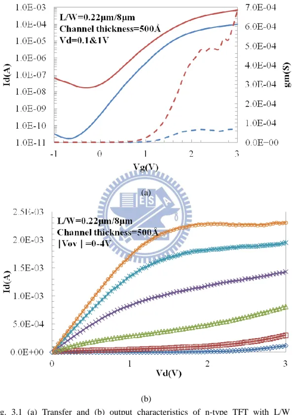
thicknesses and widths. Figures 3.1 and 3.2 show the transfer and output
characteristics of n-type TFTs with nominal gate length of 0.22μm and various gate widths of 8 and 64μm, respectively. The devices were patterned with the SP method mentioned in last chapter. The former device contains only one gate stripe, while the
latter is of interdigital type with eight gate stripes connected together. The on-to-off
current ratio (Ion/Ioff) at Vd = 0.1V is about 107, and the maximum transconductance
(gm) is about 0.68mS at gate voltage of 3V in saturation region for the device with
gate width of 8 μm as shown in Fig. 3.1 (a). Figure 3.2 (a) shows that the Ion/Ioff is
about 107 at Vd = 0.1V and the maximum gm is around 6 mS at gate voltage of 2.6V
with gate width of 64 μm. The output characteristics with different gate widths are shown in Fig. 3.1 (b) and 3.2 (b). Certainly, the more the gate width increases, the
more Ion and Ioff gain. However, the currents in Fig. 3.2 (b) are not exactly 8 times
16
dimensions. Nonetheless, the deviation from the dependency of the number of gates is
not huge as compared with the case with DP technique which will be shown in the
next paragraph.
Table 3.1 summarizes the current drive and gm of n-type TFTs with various
channel thicknesses and widths. Compared with channel thickness of 500Å , the value
of Id and gm become larger, in channel thickness of 1000Å structure, owing to the
effect of grain size of the channel thickness. The grain size is difference at different
channel thickness. The grain size is larger with channel thickness of 1000Å .
Figure 3.3 shows the transfer characteristics of devices fabricated with SP and
DP techniques at Vd = 0.1V. The SEM images of the two devices are shown in Fig. 2.7
and as mentioned in last chapter that the patterned gates show larger fluctuation with
the SP method. Summary of the measured gate length of the eight gate fingers of the
two devices with nominal gate length of 0.22μm is listed and compared in Table 3.2.
As can be seen in the Table that the finer gate patterns of the DP device can be even
shorter than 0.22μm. These “short” gates tend to increase the off-state current owing
to short channel effects, therefore the DP device exhibits an Ioff three orders of
magnitude higher than that of the SP one at Vd = 0.1V. Other major impact resulted by
the fluctuation in gate length is the degradation in the gm value, as shown in the figure.
17
3-2 Small-Signal Modeling
3-2-1 Modeling Setup Flowchart
The flowchart of complete small-signal model setup strategy [3.1] is shown in
Fig. 3.4. Following the flowchart, a complete small-signal model is established
successfully for our n-type poly-Si TFTs. In the next section, we will extract extrinsic
and intrinsic parameters step by step and compare them with the results of simulation.
3-2-2 Extrinsic Parameter Extraction
The small-signal equivalent circuit of an n-type TFT is shown in Fig. 3.5. First,
the parasitic resistances (Rg, Rd, Rs) were extracted through the cold model [3.2]-[3.5].
The small-signal equivalent circuit was transformed into the cold model when Vgs =
Vds = 0V. This bias condition causes the voltage-dependent current generator to
become zero and the output resistance (ro) to become infinite. Different from the bulk
MOSFET without substrate loss, partial depletion in the channel of the device
necessitates the consideration of the non-quasi-state effect [3.6]. The coupling path
formed between the source and drain through the quasi-neutral body region causes the
resistances expression to become frequency dependent. Cross-sectional view of an
n-type TFT with partial depletion under the zero condition and the equivalent circuit
18
is constituted by the source-side and drain-side junction capacitances (Cj,bs and Cj,bd),
and body conductances (Gbs and Gbd) [3.4][3.5]. Based on the equivalent circuit, the
parasitic resistances of the cold model can be measured by the real component of Z
parameters, which can be written as
, (3.1)
, (3.2)
, (3.3)
where Ag, As, Ad, and B are constant values at fixed bias. The existence of neutral
body may cause the parasitic resistances to become frequency dependent. It can
explain why the resistance-vs.-frequency curves are not the same as those for
conventional MOSFETs. When the frequency approaches infinity, the parasitic
resistance components can be extracted. After the extraction of extrinsic parameters,
this can be carried out using the following procedure as shown in Fig. 3.7 [3.3]. First,
the S parameters of the device are measured as shown in Fig 3.7 (a). The S parameters
are then transferred to Z parameters by subtracting Rg, Rd and Rs which are in series,
as shown in Fig 3.7 (b). The Z parameters are further transferred to Y parameters and
19
3-2-3 Intrinsic Parameter Extraction
The small-signal model of intrinsic Y parameters is shown in Fig. 3.8. The
analysis is based on the definition of Y parameters and it can be described as below:
, (3.4)
, (3.5)
, (3.6)
. (3.7)
The intrinsic parameters of small-signal model as a function of their Y parameter,
Yi, are shown below:
, (3.8) , (3.9) , (3.10) , (3.11) , (3.12) . (3.13)
20
of the imaginary part of Y parameters versus frequency multiplied by gm. The cross
section of an n-type TFT with the corresponding parasitic parameters of small-signal
equivalent circuit is shown in Fig. 3.9.
3-3 Experiment and Simulation Analyses
Theoretically extrinsic elements are bias-independent. When Vds = 0V and Vgs <
Vth, the TFT is in the cut-off state. In the cut-off state, as shown in Fig. 3.10, the real
parts of Z parameters for a device with channel thickness of 100 nm (L = 0.22μm, W
= 8μm) operated at Vds/Vgs = 0/0V and Vds/Vgs = 0/-1V are shown as a function of
frequency. The results decrease with increasing frequency and approach constant
values (i.e., Rd, Rs, and Rg), as predicted by Eqs. (3.1)-(3.3). Given the condition of
cut-off state, the values of extrinsic resistances gradually become stable as the
frequency increases. We also use this scheme to determine the extrinsic resistances for
a device with channel thickness of 50 nm (L = 0.22μm, W = 8μm) at Vds = Vgs = 0V
and the results are shown in Fig. 3.11. It is found that the extrinsic parameters are Rg =
120.33Ω, Rd = 129.41Ω, and Rs = 8.182Ω.
After subtracting extrinsic parameters, the intrinsic Y parameters can be
calculated. Intrinsic elements are theoretically bias-dependent and
21
(3.8)-(3.10). The imaginary part of the experimentally measured Y parameters linearly
increases with angular frequency as shown in Fig. 3.12 The imaginary part of Y
parameters increases with increasing frequency and the slopes of the curves approach
constant values (i.e., Cgs, Cds, and Cgd), as predicted by Eqs. (3.8)-(3.10). The gm and
ro as a function of angular frequency are shown in Fig. 3.13. Since the variation of gm
with angular frequency is small, we can determine it as the mean value in low
frequency range, e.g., < 10GHz. From Eq. (3-11), the ro is inversely proportional to
and usually is very small. Thus, a small variation in will cause a dramatic change in ro. The following item determined from the imaginary part
of the experimentally measured Y parameters, , is divided by gm
(or ) and shown in Fig. 3.14 as a function of the angular frequency. From Eq.
(3-12), the slope of the curve is τ, which indicates the mean delay time when gate bias
and gm change asynchronously. According to the above procedure we obtain the
results of intrinsic parameters of the n-type poly-Si TFT (channel thickness = 500Å , L
= 0.22μm, W = 8μm) including Cgs = 6.668fF, Cgd = 2.479fF, Cds = 2.105fF, gm =
0.489mS, ro = 3663Ω, and τ = 1.314psec. Moreover, ft is 8.074GHz and fmax is
11.69GHz, obtained from the measurement of S parameters as shown in Fig. 3.15.
In order to verify the accuracy of the small-signal model, we use the software “Advanced Design System (ADS)” (Agilent Technologies) to simulate and compare
22
with the experimental results. The frequency range is set to be from 0.2GHz to 40GHz
at Vd = 2V and Vg = 4V. We apply the extracted parameters in the small-signal model
to simulate and compare the outcome with measured results of S parameters in Fig.
3.16. As can be seen in the figure that the simulation results correspond well with the
measured data, confirming that the small-signal model is accurate.
One thing should be noted in the above results is that Rd is obviously larger than
Rs. Considering the fact that the device is symmetrical in structure, Rs and Rd should
be identical. This weird trend is attributed to the layout of the test structure and the
measurement scheme. The layout of the test device is asymmetrical after the
de-embedding process as shown in Fig. 2.6. The error arisen during the de-embedding
process is also an issue. Additionally, the grain boundary of poly-Si should also affect
the resistance.
The above procedure is also applied to a device with channel thickness = 1000Å
(L = 0.22μm, W = 8μm) and the results are shown in Figs. 3.17-3.20. Similar trends
are observed for this device and the results are Rg = 107.93Ω, Rd = 119.932Ω, and Rs
= 7.879Ω for extrinsic parameters, and Cgs = 7.264fF, Cgd = 2.26fF, Cds = 2.413fF, gm
= 0.705mS, ro = 2207Ω, and τ = 1.189psec for intrinsic parameters. The ft is
11.159GHz and fmax is 15.856GHz from the measurement of S parameters at Vd = 2V
23
parameters is shown in Fig. 3.22.
Table 3.3 summarizes the small-signal parameters of the n-type poly-Si TFTs
with various channel thickness and width. Broadening the gate width is expected to
improve the ac characteristics. Although gm has been improved, the values of parasitic
resistance become smaller but the values of parasitic capacitance increase. The gain in
resistance components is balanced but the net effect is beneficial for improving ft and
fmax.
Both ft and fmax are bias-dependent. An example for ft is shown in Fig. 3.23. The
gm increases with increasing Vd, leading to an improved ft as Vd increases. Moreover,
as compared with Vg, Vd is much more influential to ft. As the extrinsic parameters (Rg,
Rd, and Rs) are ignored, ft and fmax can be respectively expressed as
, (3.14)
. (3.15)
Although the extrinsic resistances are large and may affect the practical ac
performance, the above analysis is confirmed with the simulation results and proved
to be reliable. Major small-signal parameters extracted at Vd = 2V and various Vg are
shown in Fig. 3.24. The corresponding ft and fmax were also measured and shown in
24
Vg = 1V and compares the experimental results with the theoretical predictions made
by Eqs. (3.14) and (3.15). It is observed that the trends of calculation agree well with
25
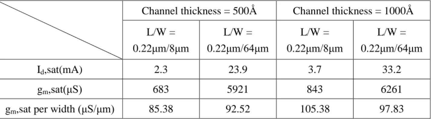
Table 3.1 Summary of basic electrical characteristics of n-type TFTs with various channel thicknesses and widths.
Channel thickness = 500Å Channel thickness = 1000Å L/W = 0.22μm/8μm L/W = 0.22μm/64μm L/W = 0.22μm/8μm L/W = 0.22μm/64μm Id,sat(mA) 2.3 23.9 3.7 33.2 gm,sat(μS) 683 5921 843 6261
gm,sat per width (μS/μm) 85.38 92.52 105.38 97.83
Table. 3.2 Measured dimensions of poly-Si gates patterned with SP or DP method with nominal gate length of 0.22μm.
The order of the gate in the
interdigital structure from left side DP SP
Number 1 gate 0.185μm 0.210μm Number 2 gate 0.260μm 0.233μm Number 3 gate 0.182μm 0.222μm Number 4 gate 0.253μm 0.234μm Number 5 gate 0.174μm 0.229μm Number 6 gate 0.259μm 0.215μm Number 7 gate 0.178μm 0.229μm Number 8 gate 0.260μm 0.231μm
26
Table 3.3 Summary of the small-signal parameters of n-type poly-Si TFTs with various channel thickness and width.
Vd = 2V, Vg = 4V Vd = 2V, Vg = 2V Channel thickness = 500Å L/W=0.22μm/8μm Channel thickness = 500Å L/W=0.22μm/64μm Channel thickness = 1000Å L/W=0.22μm/8μm Channel thickness = 1000Å L/W=0.22μm/64μm Rg(Ω) 120.33 18.25 107.93 19.68 Rd(Ω) 129.41 13.92 119.932 15.02 Rs(Ω) 8.182 1.092 7.879 1 Cgs(fF) 6.668 42.708 7.264 41.338 Cgd(fF) 2.479 17.777 2.26 17.756 Cds(fF) 2.105 8.1 2.413 10.576 gm(mS) 0.489 4.356 0.705 6.771 ro(Ω) 3663 171.891 2207 335 τ(psec) 1.314 1.043 1.189 0.893 ft(GHz) 8.074 11.499 11.159 17.123 fmax(GHz) 11.69 11.194 15.856 21.515
27
Chapter 4
Conclusion and Future Work
4-1 Summary and Conclusion
In this thesis, we have successfully fabricated and studied the RF characteristics
of n-type poly-Si TFTs. An I-line-based DP process was developed and used in the
fabrication of the devices. Resistances of source, drain, and gate were reduced with
the aid of Ni silicidation technique and implant-to-silicide scheme. RF characteristics
of the fabricated devices were characterized and a small-signal model was developed
to extract and analyze major parameters.
The characterized devices are with either single or interdigital gate pattern. For
devices with identical nominal gate length and various gate width, Ion and Ioff increase
reasonably with increasing gate width. However, the drain currents are not strictly
proportional to the gate width, owing to the effect of fluctuation of the gate
dimensions. The issue is postulated to be resulted from the poor dimension control of
the patterns on the two reticles used for the DP process. Severe fluctuation in the
dimensions of the final poly-Si gate patterns in the interdigital gate structures is
28
current owing to the short channel effects.
We’ve also successfully extract small-signal parameters by small-signal model. The simulation results of S parameters agree well with the measured data, confirming
that the small-signal model is accurate. We have also studied the variation of
parameters at different condition. As compared with the device with single-gate
pattern, the values of parasitic resistance become smaller but the values of parasitic
capacitance increase in the interdigital gate structure. In addition, the extrinsic
resistances are large and may affect the practical ac performance.
4-2 Future Work
There remain some issues to be addressed in this work. It has been demonstrated
that the parasitic components would affect RF characteristics and thus it is essential to
reduce these parasitic components. Further optimization of the silicidation process can
help. Adoption of low-resistance metallic gate materials or novel gate structures is
useful to reduce the gate resistance. Refining the re-crystallization to increase grain
size of the poly-Si films represents another useful approach for device performance
improvement.
29
parasitic parameters. The layout of the through test-structure is needed for
de-embedding procedure. The through test-structure can improve the accuracy of
de-embedding procedure. On the other hand, tighter CD control during the
manufacturing of the reticles for the DP process can help reduce the fluctuation in the
dimensions of the final poly-Si gate patterns in the interdigital gate structures. The DP
technique is also feasible for producing asymmetric S/D structure in the fabricated
n-type poly-Si TFTs. Extra freedoms offered by the asymmetric scheme in the
optimization of device structure should be a viable way for further boosting the RF
30
References
Chapter 1
[1.1] P. K. Weimer, “The TFT-a new thin-film transistor,” Proceedings of the IRE, vol. 50, no. 6, pp. 1462-1469, 1962.
[1.2] C. H. Fa, and T. T. Jew, “The poly-silicon insulated-gate field-effect transistor,” IEEE Transactions on Electron Devices,vol. 13, no. 2, pp. 290-291, 1966.
[1.3] Y. J. E. Chen, Y. J. Lee, and Y. H. Yu, “Investigation of polysilicon thin-film transistor technology for RF applications,” IEEE Transactions on Microwave
Theory and Techniques, vol. 58, no. 12, pp. 3444-3451, 2010.
[1.4] T. Serikawa, S. Shirai, A. Okamoto, and S. Suyama, “Low-temperature fabrication of high-mobility poly-Si TFTs for large-area LCD’s,” IEEE
Transactions on Electron Devices, vol. 36, no. 9, pp. 1929-1933, 1989.
[1.5] K. Werner, “The flowering of flat displays,” IEEE Spectrum, vol. 34, no. 5, pp. 40-49, 1997.
[1.6] S. Zhang, C. Zhu, J. K. O. Sin, J. N. Li, and P.K.T. Mok, “Ultra-thin elevated channel poly-Si TFT technology for fully-integrated AMLCD system on glass,”
IEEE Transactions on Electron Devices, vol. 47, no. 3, pp. 569-575, 2000.
[1.7] C. H. Tu,T. C. Chang, P. T. Liu, C. Y. Yang, L. W. Feng, C. C. Tsai, L. T. Chang, Y. C. Wu, S. M. Sze, and C. Y. Chang, “Improved performance of F-ions-implanted poly-Si thin-film transistors using solid phase crystallization and excimer laser crystallization,” Journal of Display Technology, vol. 3, no. 1, pp. 44-51, 2007.
31
fabrication by metal-induced lateral crystallization,” IEEE Electron Device
Letters, vol. 17, no. 4, pp. 160-162, 1996.
[1.9] K. Yoneda, R. Yokoyama, and T. Yamada, “Development trends of LTPS TFT LCDs for mobile applications,” IEEE Symposium on VLSI Circuits, pp. 85-90, 2001.
[1.10] S. I. Hsieh, H. T. Chen, Y. C. Chen, C. L. Chen, and Y. C. King, “MONOS memory in sequential laterally solidified low-temperature poly-Si TFTs,”
IEEE Electron Device Letters, vol. 27, no. 4, pp. 272-274, 2006.
[1.11] N. D. Young, G. Harkin, R. M. Bunn, D. J. McCulloch,.R. W. Wilks, and A. G. Knapp, “Novel fingerprint scanning arrays using polysilicon TFT’s on glass and polymer substrates,” IEEE Electron Device Letters, vol. 18, no. 1, pp. 19-20, 1997.
[1.12] I. A. Young, J. K. Greason, and K. L. Wong, “A PLL clock generator with 5 to 110 MHz of lock range for microprocessors,” IEEE Journal of Solid-State
Circuits, vol. 27, no. 11, pp. 1599-1607, 1992.
[1.13] J. Craninckx, and M. S. J. Steyaert, “A 1.8-GHz low-phase-noise CMOS VCO using optimized hollow spiral inductors,” IEEE Journal of Solid-State Circuits, vol. 32, no. 5, pp. 736-744, 1997.
[1.14] T. K. Nguyen, C. H. Kim, G. J. Ihm, M. S. Yang, and S. G. Lee, “CMOS low-noise amplifier design optimization techniques,” IEEE Transactions on
Microwave Theory and Techniques, vol. 52, no. 5, pp. 1433-1442, 2004.
[1.15] H. C. Yuan, G. K. Celler, and Z. Ma, “7.8-GHz flexible thin-film transistors on a low-temperature plastic substrate,” Journal of Applied Physics, vol. 102, no. 3, 034501, 2007.
[1.16] Y. H. Yu, Y. J. Lee, Y. H. Li, C. H. Kuo, C. H. Li, Y. J. Hsieh, C. T. Liu, Y. J. E. Chen, “An LTPS TFT demodulator for RFID tags embeddable on panel
32
displays,” IEEE Transactions on Microwave Theory and Techniques, vol. 57, no. 5, 1356-1361, 2009.
[1.17] S. L. Zhang, and M. Ö stling, “Metal silicides in CMOS technology: past, present, and future trends,” Critical Reviews in Solid State and Materials
Sciences, vol. 28, no. 1, pp.1-129, 2003.
[1.18] R. T. Tung, “Surface nucleation of Ti silicides at elevated temperatures,”
Applied Physics Letters, vol. 68, no. 14, pp. 1933-1935, 1996.
[1.19] G. G. Shahidi, J. Warnock, A. Acovic, P. Agnello, C. Blair, T. Bucelot, A. Burghartz, E. Crabbe, J. Cressler, P. Coane, J. Comfort, B. Davari, S. Fischer, E. Canin, S. Gittleman, J. Keller, K. Jenkins, D. Klaus, K. Kiewtniak, T. Lii, P. A. McFarland, T. Ning, M. Polcari, S. Subbana, J. Y. Sun, D. Sunderland, A. C. Warren, and C. Wong, “A high performance 0.25μm CMOS,” Symposium
VLSI Technology, pp. 93-94, 1993
[1.20] J. A. Kittl, A. Lauwers, O. Chamirian, M. V. Dal, A. Akheyar, M. D. Potter, R. Lindsay, and K. Maex, “Ni- and Co-based silicides for advanced CMOS applications,” Microelectronic Engineering, vol. 70, no. 2-4, pp. 158-165, 2003.
[1.21] A. Lauwers, P. Besser, T. Gutt, A. Satta, M. de Potter, R. Lindsay, N. Roelandts, F. Loosen , S. Jin , H. Bender , M. Stucchi , C. Vrancken , B. Deweerdt , and K. Maex, “Comparative study of Ni-silicide and Co-silicide for sub 0.25-μm technologies,” Microelectronic Engineering, vol. 50, no. 1-4, pp. 103-116, 2000.
[1.22] T. Morimoto, H. S. Momose, T. Iinuma, I. Kunishima, K. Suguro, H. Okano, I. Katakabe, H. Nakajima, M. Tsuchiaki, M. Ono, Y. Katsumata, and H. Iwai, “A NiSi salicide technology for advanced logic devices,” Technical
33
[1.23] H. Iwai, T. Ohguro, and S. I. Ohmi, “NiSi salicide technology for scaled CMOS,” Microelectronic Engineering, vol. 60, no. 1-2, pp. 157-169, 2002. [1.24] J. Luo, D. Wu, Z. Qiu, J. Lu, L. Hultman, M. Ö stling, and S. L. Zhang, “On
different process schemes for MOSFETs with a controllable NiSi-based metallic source/drain,” IEEE Transactions on Electron Devices, vol. 58, no. 7, pp. 1898-1906, 2011.
[1.25] A. Lauwers, J. A. Kittl,M. J.H. V. Dal, O. Chamirian, M. A. Pawlak, M. D. Potter, R. Lindsay, T. Raymakers, X. Pages, B. Mebarki, T. Mandrekar, and K. Maex, “Ni based silicides for 45nm CMOS and beyond,” Materials Science
and Engineering: B, vol. 114-115, pp. 29-41, 2004.
Chapter 2
[2.1] H. C. Lin, T. I. Tsai, T. S. Chao, M. F. Jian, and T. Y. Huang, “Fabrication of sub-100-nm metal-oxide-semiconductor field-effect transistors with
asymmetrical source/drain using I-line double patterning technique,” J. Vac.
Sci. Technol. B, vol. 29, no. 2, pp. 021007- 021007-7, 2011.
[2.2] A. Davidson, E. Strid, and K. Jones, “Achieving greater on-wafer S-parameter accuracy with the LRM calibration technique,” 34th ARFTG Conference
Digest-Winter, vol. 16, pp. 61-66, 1989.
[2.3] M. Nishimoto, M. Hamai, J. Laskar, andR. Lai, “On-wafer calibration techniques and applications at V-band,” IEEE Microwave and Guided Wave
Letters, vol. 4, nol. 11, pp. 370-372, 1994.
[2.4] M. C. A. M. Koolen, J. A. M. Geelen, and M. P. J.G. Versleijen, “An improved de-embedding technique for on-wafer high-frequency
characterization,” Bipolar Circuits and Technology Meeting, pp. 188-191, 1991.
34
Chapter 3
[3.1] S. H. M. Jen, C. C. Enz, D. R. Pehlke, M. Schroter, and B. J. Sheu, “Accurate modeling and parameter extraction for MOS transistors valid up to 10 GHz,”
IEEE Transactions on Electron Devices, vol. 46, nol. 11, pp. 2217-2227, 1999.
[3.2] D. Lovelace, J. Costa, and N. Camilleri, “Extracting small-signal model parameters of silicon MOSFET transistors,” IEEE MTT-S International
Microwave Symposium Digest, vol. 2, pp. 865-868, 1994.
[3.3] G. Dambrine, A. Cappy, F. Heliodore, and E. Playez, “A new method for determining the FET small-signal equivalent circuit,” IEEE Transactions on
Microwave Theory and Techniques, vol. 36, nol. 7, pp. 1151-1159, 1988.
[3.4] S. C. Wang, P. Su, K. M. Chen, C. T. Lin, V. Liang, and G. W. Huang, “On the RF extrinsic resistance extraction for partially-depleted SOI MOSFETs,” IEEE
Microwave and Wireless Components Letters, vol. 17, nol. 5, pp. 364-366,
2007.
[3.5] S. Lee, H. K. Yu, C. S. Kim, J. G. Koo, and K. S. Nam, “A novel approach to extracting small-signal model parameters of silicon MOSFET's,” IEEE
Microwave and Guided Wave Letters, vol. 7, nol. 3, pp. 75-77, 1997.
[3.6] A. Bracale, V. Ferlet-Cavrois, N. Fel, D. Pasquet, J. L. Gautier, J. L. Pelloie and J. du Port de Poncharra, “A new approach for SOI devices small-signal parameters extraction,” Analog Integrated Circuits and Signal Processing, vol. 25, nol. 2, 2000.
35
Figures
(a) (b)
(c) (d)
(e) (f)
36
Fig. 2.2 In-line SEM image of patterned PR lines with Lmask of 0.25μm located at
37
Fig. 2.3 In-line SEM image of patterned PR lines with Lmask of 0.25μm located at
38
Fig. 2.4 In-line SEM image of patterned poly-Si lines located at different dies of a wafer after stripping off the trimmed PR.
39
Fig. 2.5 Cross-sectional TEM image of a n-type TFT device.
40
(a)
(b)
Fig. 2.7 In-line SEM images of poly-Si gates patterned with (a) DR techniques with severe fluctuation and (b) SP techniques with greatly reduced fluctuation.
41
Fig. 2.8 Cumulative plots of measured dimensions of poly-Si gates patterned at different dies of a wafer with SP or DP methods with nominal gate length of 0.23μm.
Fig. 2.9 Equivalent circuit diagram used for the two-step correction including parasitic effect [2.2].
0.1
0.2
0.3
0.4
C
um
ul
a
ti
v
e
pr
o
ba
bi
li
ty
(fr
o
m
0
to
1)
Gate length(μm)
Single pattering
Double patterning
42
(a) (b)
Fig. 2.10 (a)The open test fixture and (b) the diagram of equivalent circuit.
(a) (b)
43
(a)
(b)
Fig. 3.1 (a) Transfer and (b) output characteristics of n-type TFT with L/W = 0.2μm/8μm.
44
(a)
(b)
Fig. 3.2 (a) Transfer and (b) output characteristics of an SP n-type TFT with L/W = 0.2μm/64μm.
45
Fig. 3.3 Transfer characteristics of n-type TFTs at Vd = 0.1V patterned with SP and
DP techniques. Nominal gate length and width are equal to 0.22μm and 64μm, respectively.
46
Fig. 3.4 The flowchart of small-signal model setup.
47
(a)
(b)
Fig. 3.6 (a) Cross-sectional view of n-type TFTs with a partially depleted channel under the zero condition and (b) the equivalent circuit model.
48
↓
S→Z
(a)↓
Z→Y
(b)
49
Fig. 3.8 Intrinsic part of an n-type TFT.
Fig. 3.9 The cross section of an n-type TFT with corresponding small-signal equivalent circuit.
50
Fig. 3.10 Modeling results for extrinsic resistance extraction considering the neutral-body effect at cut-off condition for a device with channel thickness of 1000Å . (lines: Vd = 0V and Vg = -1V. symbols: Vd = Vg = 0V)
Fig. 3.11 Modeling results for extrinsic resistance extraction considering the neutral-body effect at cut-off condition for a device with channel thickness of 500Å .
51
Fig. 3.12 Modeling results for Im(Y11+Y12), -Im(Y12), and Im(Y22+Y12) for a device
with channel thickness of 500Å .
52
Fig. 3.14 Modeling results for τ for a device with channel thickness of 500Å .
53
(a)
(b)
Fig. 3.16 Modeling results of (a) S11 and S22 and (b) S12 and S21 at Vd = 2V and Vg =
4V. (lines for measurements, symbols for models, channel thickness = 500Å ,and L/W = 0.22μm/8μm)
54
Fig. 3.17 Modeling results for extrinsic resistance extraction considering the neutral-body effect at cut-off condition for a device with channel thickness = 1000Å
Fig. 3.18 Modeling results of Im(Y11+Y12), -Im(Y12), and Im(Y22+Y12) for a device
55
Fig. 3.19 Modeling results of gm, and ro for a device with channel thickness = 1000Å
56
57
(a)
(b)
Fig. 3.22 Modeling results of (a) S11 and S22 and (b) S12 and S21 at Vd = 2V and Vg =
2V. (lines for measurements, symbols for models, channel = 1000Å ,and L/W = 0.22μm/8μm)
58
Fig. 3.23 ft measured at Vd = 1V and 2V for a device with channel thickness of
59
(a)
(b)
Fig. 3.24 Small-signal parameters extracted at Vd = 2V and various Vg for a device
60
Fig. 3.25 The ft and fmax measured at Vd = 2V and various Vg for a device with channel
thickness of 1000Å .
Fig. 3.26 Comparisons between analytical calculation (lines) and measured ft and fmax