國立交通大學
電子工程學系 電子研究所碩士班
碩士論文
使用
I-Line 雙重曝光技術實現非對稱 0.1μm P 型
金氧半場效電晶體與相關可靠度問題之研究
A Study of Double-Patterning Technique with
i-line Stepper to accomplish 0.1μm PMOSFETs
and Its Related Reliability Issues
研 究 生:張博翔
指導教授:林鴻志 博士
黃調元 博士
使用
I-Line 雙重曝光技術實現非對稱 0.1μm P 型金
氧半場效電晶體與相關可靠度問題之研究
A Study of Double-Patterning Technique with i-line
Stepper to accomplish 0.1μm PMOSFETs and Its
Related Reliability Issues
研 究 生:張博翔 Student: Po-Hisang Chang
指導教授:林鴻志 博士 Advisors: Dr. Horng-Chih Lin
黃調元 博士 Dr. Tiao-Yuan Huang
國立交通大學
電子工程學系 電子研究所碩士班
碩士論文
A Thesis
Submitted to Department of Electronics Engineering and Institute of Electronics College of Electrical and Computer Engineering
National Chiao-Tung University
in Partial Fulfillment of the Requirements for the Degree of Master in Electronics Engineering
September 2010
Hsinchu, Taiwan, Republic of China
使用
I-Line雙重曝光技術實現非對稱0.1μm P型
金氧半場效電晶體與相關可靠度問題之研究
研究生:張博翔 指導教授:林鴻志 博士
黃調元 博士
國立交通大學
電子工程學系 電子研究所碩士班
摘要
本篇論文使用i-line光學步進機,應用雙重微影成像法之技術,製
作出遠優於i-line光學步進機解析度極限(~0.3μm) 的次0.1微米的閘極
圖形;並搭配新設計的光罩,改進先前研究遭遇到元件過度蝕刻造成
缺陷的問題[1]。這技術包含了兩次光學微影以及後續蝕刻製程。此
技術可應用在非對稱金氧半場效電晶體的結構設計與製作,其電晶體
可以比傳統的對稱結構有更大的最佳化空間。本研究調變了汲極延伸
區域的接面深度與源極/汲極邊緣的局部摻雜(halo implant),來驗
證其對於驅動電流、短通道效應的影響,最後再進行元件負偏壓溫度
不穩定性的分析研究。
A Study of Double-Patterning Technique with
i-line Stepper to accomplish 0.1μm PMOSFETs
and Its Related Reliability Issues
Student : Po-Hisang Chang Advisors : Dr. Horng-Chih Lin
Dr. Tiao-Yuan Huang
Department of Electronics Engineering & Institute of Electronics
National Chiao Tung University
Abstract
In this thesis, we developed a novel double patterning technique, which consists of two exposures with an i-line stepper and two etch steps, to define poly-Si gates with line width down to sub-100nm regime, far beyond the resolution limit of the conventional i-line lithographic method (~0.3 μm). The double patterning process has also been employed in fabrication of sub-100 nm p-channel devices. During the course, we addressed an unexpected etch-induced recess phenomenon encountered in the study of our group in previous year [1] with ingenious modification in the mask design. We’ve also demonstrated the capability of the developed double patterning method in fabricating MOSFETs with asymmetrical S/D. The basic electrical
characteristics of the PMOSFET devices with symmetrical and asymmetrical S/D were measured and compared. The results confirm the enhancement of immunity to the short-channel effects with asymmetrical S/D design. Finally, we also explored the negative-bias-temperature-instability (NBTI) of the fabricated devices.
誌謝
在碩士生涯兩年中,首先由衷地感謝我的兩位指導教授林鴻志博士以及黃 調元博士。感謝林老師的諄諄教誨指導了我研究的方法,以及正確的求學態度, 此外老師孜孜不倦的研究精神與不忮不求的處世風範,給了我在研究上應有的態 度和熱誠的典範;而黃老師廣博的知識領域以及學術上所累積的寶貴經驗,拓展 了我的視野,也給了我許多啟發。兩位老師對學術的嚴格把關與要求,熱心且不 斷的教導與提攜,促使我成長,而兩位老師認真地批改我的論文使得論文的內容 更加的精實,若沒有兩位老師的幫忙,今天不可能完成這篇論文。 在實驗方面要感謝國家奈米元件實驗室提供的環境以及資源,同時對製程 實驗中提供意見以及幫忙的人員敬上最大的感謝,讓實驗能夠順利進行。再來是 感謝蔡子儀學長帶領者我進行製程、量測以及分析,無私的分享經驗令人獲益良 多。 在求學期間,感謝交大先進元件技術實驗室(ADTL)其他成員的幫助,與 他們共事是我的福分,因為有你們在生活上、實驗上的扶持與協助,使得我在這 間實驗室唸書兩年的路上充滿了歡樂、溫暖而不孤單。另外還要感謝李振銘、王 昭龍、章緯等其他實驗室的博班學長,給予我在論文研究上的協助,萬分慶幸有 如此多的貴人相助,在此奉上最真心的感激與祝福。 最後要深深地感謝我親愛父母親,張朝安先生以及邱金月女士,感謝他們 二十餘年來的栽培,讓我今日能夠挑戰自己,感謝他們和我分享情緒,讓我能夠 堅持到底;有了他們的全力支持,才可以讓我毫無後顧之憂地在研究上衝刺。張博翔
誌於新竹交通大學
Contents
Abstract (in Chinese)………i
Abstract (in English)………ii
Acknowledgement (in Chinese)………... iv
Contents………..….v
List of Figure Captions...vii
List of Table Captions...xi
Chapter 1 Introduction
...11-1 Background
...11-2 Double Patterning Technique
...31-3 Halo Implantation and Source/drain Extension Structure
...41-4 Motivation and Objectives of this Thesis
...61-5 Organization of This Thesis
...7Chapter 2 Device Structure, Process Flow and
Measurement Setup ...
102-1 Device Fabrication and Process Flow
...102-2 Feasibility of the Double Patterning Technique
...12Chapter 3 Results and Discussion
...163-1 Nano-Scale Device Performance and End-Point-Detection
Issue
...163-2 Basic Electrical Characteristics
...173-2-1 Electrical Characteristics of P-channel MOSFETs with
Asymmetric S/D Extension...18
3-2-2 Electrical Characteristics of P-channel MOSFETs with
Halo-implant...19
3-3 Negative Bias Temperature Instability Characteristics
...21Chapter4 Conclusion and Future Work
...254-1 Conclusions
...254-2 Future Work
...26References
... 28Figures
...33Figure Captions
Chapter 1
Fig. 1.1 Cross sectional view of a device with nominal gate length (Lmask) of 0.2 μm
fabricated with I-line DP process developed by our group in previous year [1]. Si recess resulted in the 2nd poly etch step was found at one side of the gate.. ……….33
Chapter 2
Fig. 2.1 Process flow of asymmetric extension PMOSFETs with drain-side halo-implantation.. ………35 Fig. 2.2 Design of the double-patterning masks, (a) Top view and (b) Cross-sectional
view.. ………36 Fig. 2.3 Top-view SEM images of poly-Si gates formed by single patterning
process……….37 Fig. 2.4 SEM image of a poly-Si gate with 32 nm in line width, formed by DP process
with designed line width of 50 nm.. ………..38 Fig 2.5 Top-view SEM image of a poly-Si gate with designed line width of 50 nm
formed by double patterning process.. ………..38 Fig. 2.6 Top-view SEM image of a poly-Si gate with designed line width of 60 nm
formed by double patterning process.. ………..38 Fig. 2.7 Top-view SEM image of a poly-Si gate with designed line width of 80 nm
formed by double patterning process.. ………...39 Fig. 2.8 Top-view SEM image of a poly-Si gate with designed line width of 0.1 μm
Fig. 2.9 Top-view SEM image of a poly-Si gate with designed line width of 0.12 μm formed by double patterning process. ………..…..….………..39 Fig. 2.10 Top-view SEM image of a poly-Si gate with designed line width of 0.14 μm
formed by double patterning process. ………..…40 Fig. 2.11 Top-view SEM image of a poly-Si gate with designed line width of 0.2 μm formed by double patterning process. ………..…………40 Fig. 2.12 Top-view SEM image of a poly-Si gate with designed line width of 0.3 μm
formed by double patterning process.. ……….…………40 Fig. 2.13 Practical gate length (Lgate) extracted by top-view SEM images versus the
designed gate length (Lmask). The error bar indicates the standard deviation
(1-σ) of the measured data.. ………41 Fig. 2.14 Measurement setup……….. ………42
Chapter 3
Fig. 3.1 Cross sectional view of the DP gate with designed gate length Lmask = 0.1
μm. ………...…….43 Fig. 3.2 Transfer characteristics of (a) Id-Vg and (b) Id-Vd with practical gate length of
85 nm and width of 10 μm. ……….……….43 Fig. 3.3 Schematic illustrations of the DP gate patterns formed after G1 and G2
etching steps with (a) old and (b) new G1 mask design..………..44 Fig. 3.4 Cross-sectional view of the fabricated MOSFET showing the damaged region caused by the second (G2) etching. [1]…...………..45 Fig. 3.5 (a) Type A device serves as the control samples with symmetric S/D. (b) Type
B device with shallower drain extension.………..46 Fig. 3.6 (a) Type C device with drain-side-only halo. (b) Type D device with
symmetrical halo.. ………46 Fig. 3.7 The CV curve of an asymmetric PMOSFET with DP process. The
measurement frequency is 100 kHz……..……….……….…..46 Fig. 3.8 (a) Typical transfer and (b) output characteristics of Type A and Type B
devices with channel length of 0.1 μm and channel width of 10 μm……….………47 Fig. 3.9 Transconductance (Gm) of Type A and Type B devices with channel length of
0.1 μm and channel width of 10 μm.………..……..48 Fig. 3.10 Threshold voltage of Type A and Type B devices as a function of channel
length……… …..……….….48 Fig. 3.11 Extracted values of external S/D resistance of (a) Type A and (b) Type B
devices are 170 Ω and 240 Ω, respectively………..49 Fig. 3.12 Transfer characteristics of Type A devices with various channel length
ranging from 0.08 to 10 μm. All devices have the same width of 10 μm. (a)
Vd =-1.5 V. (b) Vd = -0.05 V………50
Fig. 3.13 Transfer characteristics of Type C devices with various channel length ranging from 0.08 to 10 μm. All devices have the same width of 10 μm. (a)
Vd =-1.5 V. (b) Vd = -0.05 V. ……..………..………51
Fig. 3.14 Transfer characteristics of Type D devices with various channel length ranging from 0.08 to 10 μm. All devices have the same width of 10 μm. (a)
Vd =-1.5 V. (b) Vd = -0.05 V……….………...……….52
Fig. 3.15 Threshold voltage shift as a function of channel length for Types A, C, and D samples. ……….…...53 Fig. 3.16 DIBL as a function of channel length for Types A, C, and D
Fig. 3.17 On-current at Vg-Vth = -2V as a function of channel length for Types A, C,
and D samples……….………..54 Fig. 3.18 Schematic structure of the SiO2/Si interface [29].………...……….55
Fig. 3.19 Vth shift-versus-stress time curves for Type A devices with various channel
length 0.14 μm, 1 μm and 10 μm at 125 o
C…….…….……….55 Fig. 3.20 A proposed scheme for passivation of interface states with F from the S/D
extension of PMOSFET devices with (a) long-channel length and (b) short-channel length………..56 Fig. 3.21 Subthrehold characteristics measured and 25 o
C or 125 o
C for Type A devices with channel length of 0.14 μm and 10 μm before and after NBTI stress with gate voltage of -3.3 V………... ………56 Fig. 3.22 Vth shift-versus-stress time curves for Type A device with channel length
0.14 μm at 25 o
C, 75 o
C and 125 o
C……...……….... ……….57 Fig. 3.23 Vth shift-versus-stress time curves for Type A device channel length 0.14
μm at 125 o
C and with various stress gate voltage -2.3 V, -2.8 V, and -3.3 V……….. ……….57 Fig. 3.24 Vth shift-versus-stress time curves for Type A and Type D devices with
channel length 0.14 μm at 25 o
C, 75 o
C and 125 o
C.…………..……….58 Fig. 3.25 Vth shift-versus-stress time curves for Type A and Type D devices at 125o
C and channel length 0.14 μm with various stress gate voltage -2.3 V, -2.8 V, and -3.3 V. ……….58
Table Captions
Table 1.1 Lithographic-Field and Wafer Size Trends [3]………..…9 Table 2.1 Split conditions of the PMOSFETs fabricated with the DP process…….…15 Table 2.2 Other major implantation conditions used in the PMOSFET fabrication.. .15 Table 2.3 Specifications of Canon FPA-3000i5+ Stepper………. …………..…15
Chapter 1 Introduction
1-1 Background
With the first commercial Si transistor announced by Texas Instruments (TI) in 1954 [2], Si quickly replaced Ge as the most important semiconductor for manufacturing. In 1970s, the “Si-based” technology had been well established. To increase the device density and reduce the fabrication cost, the IC industry had concentrated on scaling down the devices’ dimensions and enlarging the wafer size since the early 1960s. Today, the mainstream of wafer diameter has been shifted from 8 inch (200 mm) to 12 inch (300 mm), and the microprocessor unit (MPU) physical gate length of device has scaled down to nano era (< 29 nm) according to the International Technology Roadmap for Semiconductors (ITRS) 2009 (Table. 1-1) [3]. Moreover, the physical gate length of device is scaling down to 22 nm for the requirements of high-performance logic technology in 2012 [3].
Major purposes of shrinking the Metal-Oxide-Semiconductor Field-Effect Transistor (MOSFET) dimension are to enhance the driving capability and increase the device density. However, as the MOSFET dimensions are reduced, there are many issues obstructing the progress of the semiconductor device. The most well known issue is the occurrence of short channel effects (SCE) that cause the threshold voltage
(Vth) roll-off, drain-induced barrier lowing (DIBL), and bulk punch-through, etc
[4]-[16]. These effects become more difficult to suppress as the channel length decreases continuously.
Another issue is related to the lithography techniques for generating the fine patterns. Current 45 and 32 nm nodes of manufacturing need water-based 193nm immersion (193i) lithography to generate the most critical patterns. However, the cost of 193i lithography machine is above 60 million U.S. dollars [17] which is too high and not affordable for most academic organizations. Concurrently, although e-beam exposure technique is feasible to scale device gate length down to 0.1 μm, it suffers from the low throughput. To relieve these concerns, recently our group proposed the use of double patterning technique (DPT) with an i-line stepper to realize the fabrication of sub-0.1 μm devices [1] which could take advantage of much reduced cost as compared to the 193i techniques and much faster throughput as compared to the e-beam counterparts.
To alleviate the SCEs and other degradation effects caused by scaling, many researchers have devoted themselves to inventing new device structures to enhance the device performance. For example, devices with lightly-doped drain (LDD) [18] structures were utilized to decrease the hot-carrier effects (HCEs). Even with the scaled supply voltage nowadays, LDD structures are still important in input/output
(I/O) devices. Other devices with double implanted LDD (DI-LDD) [18] structures, which are also called “halo implant” structures [10]. Such structures are added with an oppositely type of dopants located near the channel and underneath the source and drain junctions to meliorate the SCEs. Thanks to the development of those structures, great advancement in semiconductor technology has been achieved and the progress is still going.
Furthermore, in order to lower process cost and simplify device fabrication, standard manufacture schemes are devised with the symmetric structure. That is, the source and drain doping profiles are the same. However, theoretically symmetric structures are not ideal for device performance, and, with an appropriate design, asymmetric structures should outperform the symmetrical counterparts.
1-2 Double Patterning Technique
As mentioned above, 193i lithography is being used for 45 nm and 32 nm nodes of manufacturing [3]. The Rayleigh equation applicable for immersion lithography can be written as IF K HP N NA ,
where HP is the minimum printable half pitch feature size, NIF is the immersion fluid
index of refraction at the lithographic wavelength, NA is the numerical aperture of the (1-1)
stepper lens, λ is the lithographic wavelength, and K is a measure of the lithographic process capability. Since the NIF of a liquid (e.g., water) is much larger than that of air,
the resolution can be improved with the wet lithographic techniques.
However, it’s very difficult for 193i to push further into 22 nm node and beyond, so finding a succeeding technique is urgent. One of the possible solutions is extreme ultra-violet (EUV) method which uses a much shorter wavelength of 13.4 nm with an NA of ~0.25. Another way is the 3rd generation immersion 193 nm system which has ~1.55 NA requiring higher refractive index (RI) (RI > 1.8) fluids, lens and photo-resists materials. Nevertheless, none of these techniques are ready for production yet to this date [20].
Double patterning (DP) is a resolution improvement technique that can potentially cut the pitch of patterns in half [21]. Double patterning lithography (DPL) has already shown its feasibility to the 22nm node [22]. Consequently, DP is viewed as a bridge to EUV lithography technology, which is not expected to be available for volume production until approximately 2011 or later.
1-3 Halo Implantation and Source/drain Extension Structure
For the purposes of performance enhancement and cost reduction, MOSFET scaling is inevitable. Certainly there are a number of critical problems lying ahead that
need to be carefully addressed [23]-[24].
Nowaday the most general method to restrain the SCE-induced drain-induced barrier lowing (DIBL), Vth roll-off, and bulk punch-through, is to perform the halo implantation (also called the pocket implantation) [19], which was first presented in 1985 and also called DI-LDD [18].
Halo implantation structure is formed using a titled angle implantation to form the high counter doping regions at the drain/substrate and source/substrate junctions and below the channel. The dopant type is the same as that of the substrate. Because of the relatively high doping concentration, the depletion regions of both source and drain extensions can be suppressed efficiently, resulting in a significant reduction in the subthreshold leakage current and the bulk punch-through, hence alleviating the SCE-induced degradations.
LDD structure [18] is used to improve HCE for devices working under a high operation voltage (e.g., I/O devices). As the applied drain voltage is sufficiently high that the maximum electric field along the channel exceeds a certain value, significant impact ionization may occur near the drain side. Fortunately, we can utilize the LDD structures to relieve the concern somewhat by decreasing the peak electric field in the channel of the MOSFET [25]. Actually LDD structures [18] have been commonly used to improve hot-carrier reliability [26]-[28] for MOSFETs operated under a high
voltage.
However, when MOS devices are scaled to nano-scale regime, the LDD regions will contribute more parasitic resistance and result in drain current degradations. Moreover, operation voltage of the core devices in most advanced chips has been lowered to around 1V. This means the HCEs is no longer a major concern for these devices. Therefore the doping concentration of the regions is increased to a level comparable to that in the deep source/drain S/D regions for reducing the parasitic resistance but the junction depth is retained ultra-shallow for good control of the SCEs. In those nano-scale devices the previous “LDD” regions are renamed as “extension” since they are no longer “lightly doped.” Furthermore, the use of asymmetric source/drain (S/D) extension (i.e., the two extensions have different doping concentration and/or junction depth) structures can be adopted for optimizing the current-drive capability, SCE control, and hot-carrier reliability [26]-[28].
1-4 Motivation and Objectives of this Thesis
As mentioned in Sec. 1-2, our group proposed the implementation of double patterning technique (DPT) into the i-line photolithographic process to realize the fabrication of nano-scale devices [1]. Basically the concept has been proved to be useful and feasible for generating patterns with critical dimension (CD) down to 0.1
μm. However, most of the devices fabricated in the previous work were found to be with poor performance and leaky. Origins for such outcome are found to be related to the etch-induced recess occurring at one side of the gate during the second gate etch step. An example is shown in Fig. 1-1. Occurrence of such phenomenon is due to the failure of end point detection during the second gate etch step. This issue has been addressed [1] and is expected to be solvable with a modified mask design. In this study, we examine the feasibility of the DP process with aforementioned modification in mask layout design and aim at fabrication and characterization of p-channel devices with channel length down to 0.1 μm and even shorter.
1-5 Organization of This Thesis
This thesis is divided into four chapters and each chapter is introduced briefly as below.
In Chapter 1, we show a brief overview of the background and the motivation. In Chapter 2, we describe and evaluate the DP process developed in this work, and then we describe the DP technique for device fabrication. Finally, we present the measurement setup and characterization scheme.
In Chapter 3, we present the experimental results on characterizing the fabricated PMOSFET devices. Transfer and output current-voltage (I-V), and
capacitance-voltage (C-V) characteristics are examined and discussed. We also explore the effects of the halo-implant, symmetric and asymmetric extension structures on the device characteristics, device reliability issue like NBTI performance.
Chapter 2 Device Structure, Process
Flow and Measurement Setup
All the device fabrications mentioned in this thesis were accomplished at the National Nano Device Laboratories (NDL).
2-1 Device Fabrication and Process Flow
In this chapter, we take the asymmetric PMOSFET with drain-side only halo as an example to illustrate the process flow in Fig. 2.1.
The devices were fabricated on 6-inch n-type bare Si wafers with resistivity of 15~25 ohm-cm. N-type well was formed by phosphorus ion (P+) implantation (at 120
keV, 7.5E12 cm-2), Vth was adjusted by arsenic ion (As+) implantation (at 80 keV,
1E13 cm-2), anti-punchthrough implantation was formed by P+ implant (at 120 keV,
4E12 cm-2), and channel stop implantation for local oxidation of silicon (LOCOS)
isolation was done by As+ implant (at 120 keV, 3E12 cm-2).
After the above standard MOSFET LOCOS and n-well processes, thermal gate oxide with a thickness of 3 nm was grown in N2O ambient, followed by a 170
nm-thick undoped polycrystalline silicon (poly-Si) deposition performed in a vertical furnace by low-pressure chemical vapor deposition (LPCVD). Subsequently, undoped
poly-Si was implanted with boron-fluoride ion (BF2+) at 15 KeV, 5E15 cm-2. Then a
50 nm-thick LPCVD TEOS oxide was deposited as a hard mask layer.
The DP technique uses two masks denoted as G1 and G2, respectively, as shown in Fig. 2.2 to define the gate. During fabrication the gate etching steps were done with a Lam-TCP9400 operated with end point detection mode. An annealing was employed using rapid thermal anneal (RTA) at 900 o
C for 10 second (s) after the G1 formation process. Then asymmetric source and drain extensions were formed separately after G1 and G2 definitions, respectively. Meanwhile, according to the demand of experimental conditions, the 45 o
tilted angle halo-implantation was done with As+ (at 15 to 30 keV, 5E12 cm-2) at drain side only, as shown in Fig. 2.1. For the
split with source-side-only halo, such implant was done immediately after the source-side extension implant. Additional split with symmetrical halo structure was also fabricated. For that split and control samples which was with symmetric S/D extension and no halo implemented, the S/D extension and halo (optional) implants were done together after G2 gate definition.
After halo implantation, 100 nm sidewall spacer was formed with LPCVD TEOS oxide, followed by deep S/D implant with BF2+ (at 40 keV, 5E15 cm-2).
Afterwards, the regions of substrate windows were formed and implanted with P+ (at
(SRTA) at 1000 o
C to activate the dopants in the preceding implantation processes. Finally, standard backend flow was executed to complete the fabrication.
The major split conditions explored in this work are listed in Table 2.1. Other implant conditions, including well implantation, threshold voltage adjustment implantations, channel stop implantation, and anti punch-through implantation are shown in Table 2.2.
2-2 Feasibility of the Double Patterning Technique
After finishing the G1 and G2 gate etching steps, we employed in-line scanning electron microscope (SEM), and focused ion-beam (FIB) SEM imaging techniques to check the test structures as well as the practical gate electrodes which were formed by either DP or single patterning technique. For all lithographic steps, we used an I-line stepper to generate the photoresist (PR) patterns, and the design of the DP masks is shown in Fig. 2.2. In this figure, the G1 mask covers the right side of the active region which is capped with the poly-Si as the gate material, and then the G2 mask covers the left side of the active region. After the two-step gate mask processes, the overlapped region of the G1 and G2 masks defines the gated region, and the gate length can be smaller than the resolution limit of single patterning technique (~0.35 μm) with conventional I-line steppers.
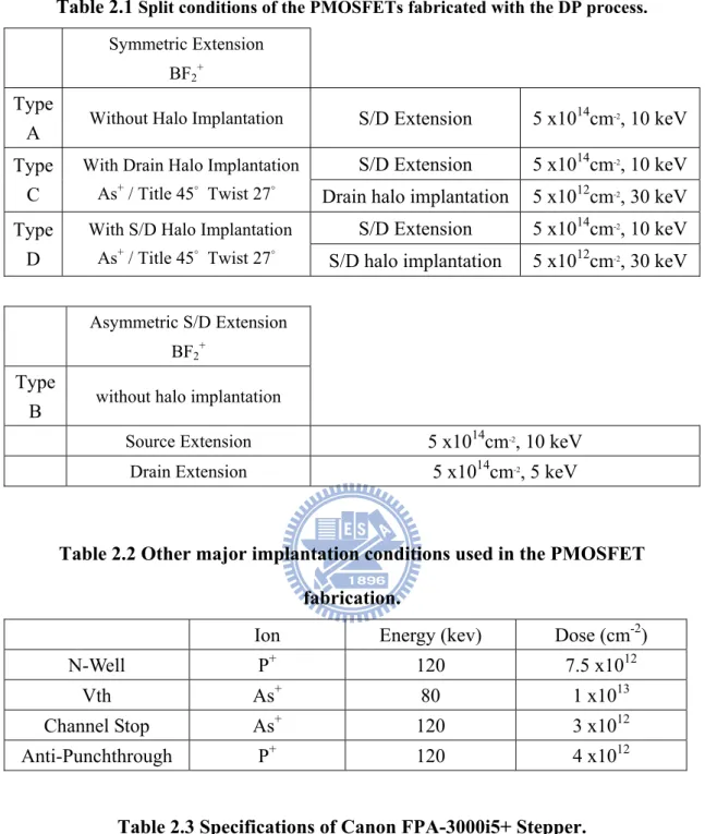
Figure 2.3 shows the gate length images which were formed by conventional single patterning technique. In the pictures, in order to evaluate the gate length error caused by the process and instrumental factors, we compare the difference between the designed or nominal length (Lmask) on mask and the practical physical length (Lgate)
of the etched poly-Si gate measured by the in-line SEM.:
mask gate ErrorL L , | | % mask gate 100% mask L L Error L .
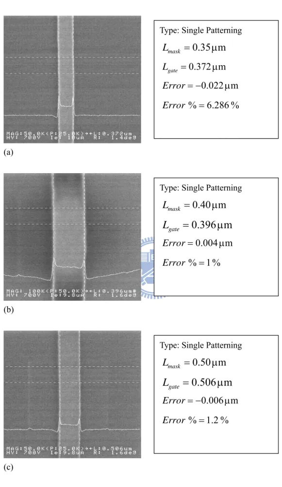
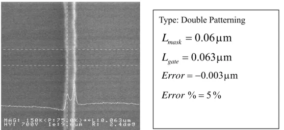
In Fig. 2.3, it is observed that the error of gate length formed with conventional I-line scheme is less than 10 %. Nonetheless, the feature size of the line is larger than 0.3 m. Figure 2.4 shows that the shortest gate length is around 32 nm with designed length of 50 nm. Figures 2.5 ~ 2.12 show the in-line SEM images of the etched poly-Si gates formed with the DP method with Lmask ranging from 60 to 300 nm. From
these figures it is confirmed that the DP can significantly shrink the feature size of the poly-Si gate down to sub-100 nm regime. Generally, the error percentage increases with decreasing Lmask. Such trend is reasonable as far as the overlay accuracy of the
i-line stepper is concerned. As shown in Table 3, the overlay accuracy is larger than 45 nm. This implies that the gate length designed below 80 nm is out of control and difficult to reproduce. Anyway, the present DP method is useful for generation of line patterns down to 80 nm with reliable control of critical dimensions, as shown in Fig. (2-1) (2-2)
2.13.
2-3 Electrical Measurement Setup
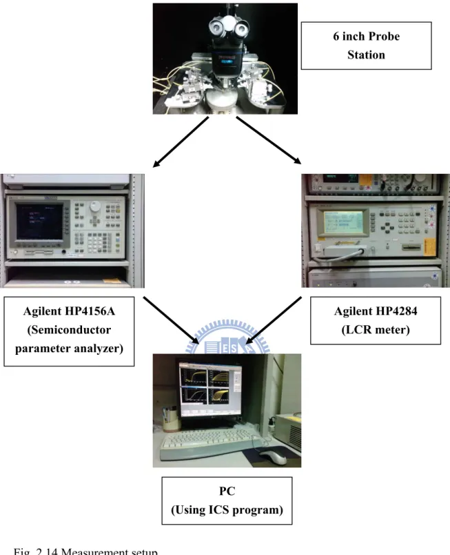
In this study, the electrical characteristics of the fabricated devices were evaluated by using a precision semiconductor parameter analyzer HP 4156A for I-V measurements and an LCR meter HP 4284 for C-V measurements. The device characteristics were measured on the 6 inch probe station at various gate voltages (Vg
= 1 ~-2V) and drain voltages (Vd = 0 ~ -2V). Fig. 2.14 shows the measurement setup
used in this experiment.
In addition to basic electrical measurements, we also analyze the device degradation and reliability, including test on static negative-bias-temperature instability. Details about the test conditions are given in the thesis as the results are presented.
Table 2.1 Split conditions of the PMOSFETs fabricated with the DP process.
Symmetric Extension BF2+
Type
A Without Halo Implantation S/D Extension 5 x10
14cm-2, 10 keV
S/D Extension 5 x1014cm-2, 10 keV Type
C
With Drain Halo Implantation As+ / Title 45° Twist 27°
Drain halo implantation 5 x1012cm-2, 30 keV S/D Extension 5 x1014cm-2, 10 keV Type
D
With S/D Halo Implantation As+ / Title 45° Twist 27°
S/D halo implantation 5 x1012cm-2, 30 keV
Asymmetric S/D Extension BF2+
Type
B without halo implantation
Source Extension 5 x1014cm-2, 10 keV
Drain Extension 5 x1014cm-2, 5 keV
Table 2.2 Other major implantation conditions used in the PMOSFET fabrication.
Ion Energy (kev) Dose (cm-2)
N-Well P+ 120 7.5 x10¹²
Vth As+ 80 1 x10¹³
Channel Stop As+ 120 3 x10¹²
Anti-Punchthrough P+ 120 4 x10¹²
Table 2.3 Specifications of Canon FPA-3000i5+ Stepper. (Data are courtesy of NDL)
Chapter 3 Results and Discussion
3-1 Nano-Scale Device Performance and End-Point-Detection
Issue
Figure 3.1 shows the cross-sectional view of a poly-Si gate with Lmask of 0.1 μm. The figure shows that the practical gate length Lgate is measured to be 85 nm. Figure
3.2 shows the characteristics of electrical measurements performed on this device. The device was fabricated with source extension formed with BF2+ implant (at 10 keV,
5E14 cm-2), drain extension formed with BF
2+ implant (at 5 keV, 5E14 cm-2), and
drain-side-only halo formed with As+ implant (at 30 keV, 5E12 cm-2, 45 degree).
With the aid of the proposed DP method, well-behaved characteristics are demonstrated in the nano-scale device.
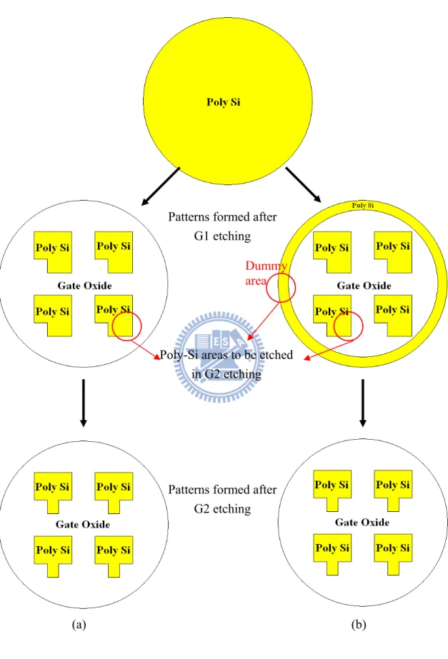
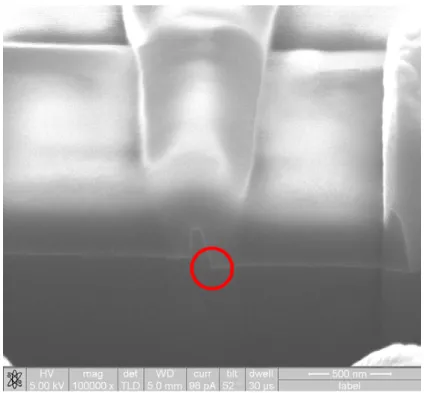
One issue encountered in our previous work [1] is illustrated in Fig. 3.3(a), which schematically shows the layout of original device design regarding G1 and G2 masks mentioned in Chap. 2. Figure 3.4 shows the cross-sectional view of a device taken in the prior study [1]. In the figure we can observe the substrate recess at the right side of the poly-Si gate. Such a phenomenon was induced during the second poly-Si etching step (with G2 mask) and had been identified to be caused by the ineffectiveness of end-point detection (EPD) technique. In the original mask design
shown in Fig. 3(a), most of the poly-Si film area will be removed during the first etching step. Therefore the EDP signal is too weak to be detected in the second etching step. The mismatch in etched profile results in high series resistance and low driving current [1]. To address this issue, in this work we modify the G1 mask by adding additional dummy regions, as shown in Fig. 3.3(b), so the total area of the poly-Si film present during the second etching step is sufficiently large for effective EPD. As the new scheme in mask design is implemented, the above issue is well resolved as evidenced in Fig. 3.1.
3-2 Basic Electrical Characteristics
Basic electrical characterization was performed on four types of devices fabricated with the DP process, as shown in Figs. 3.5 and 3.6 and denoted as Types A, B, C, and D, respectively. Details about the implant conditions of extension and halo for the four splits of devices are listed in Table 2.1. In brief, Type A has symmetrical S/D extensions, Type B has asymmetrical S/D extensions, Types C and D both have the same symmetrical S/D extensions as that of Type A, but Type C has on-side-only halo while Type D has symmetrical halo.
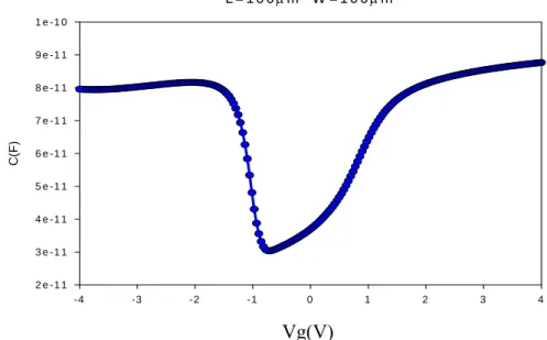
Figure 3.7 shows the CV curves of the PMOSFET measured at 100 kHz. The electrical effective oxide thickness (EOT) is 4.2 nm as estimated from the inversion
capacitance, in good agreement with the physical thickness of 3.5 nm. The result also indicates that the poly depletion effect is negligible.
3-2-1 Electrical Characteristics of P-channel MOSFETs with
Asymmetric S/D Extension
In this section, we analyze and compare the electrical characteristics of Type A and Type B shown in Figs. 3.5 (a) and (b), respectively.
As transistors are made smaller, the junctions that form the source and drain regions of the transistor must be made shallower in order to improve performance and provide adequate breakdown characteristics. In particular, the region known as the drain extension must be extremely shallow to suppress the short-channel effects. Figures 3.8(a) and (b) show and compare the transfer and output characteristics, respectively, of Type A and Type B devices with channel length of 0.1 μm and width of 10 μm. With a shallower drain extension in the Type-B device, we can see in Fig. 3.8(a) that subthreshold swing of this device is slightly improved as compared with the Type-A sample. Nonetheless, the shallower drain also introduces additional resistance, resulting in degraded drive current performance illustrated in Fig. 3.8(b). Impact of the increased series resistance also reflects on the transconductance (gm) performance, as shown in Fig. 3.9.
(W/L).10nA, where L is the channel length and W is the channel width. The figure shows that one of the familiar short-channel effects, the Vth roll-off
phenomenon, owing to the charge sharing at source and drain junctions [25]. While the drain extension becomes shallower for the Type B split as compared with the Type A, the roll-off is improved due to the decreased depletion region which reduces the charge sharing effect.
Figure 3.11 shows the extracted external S/D resistance of the two types of devices. Extraction of the parameter is based on the method proposed and developed previously [25]. From the results, we confirm that the shallower junction indeed results in a larger parasitic resistance,.
3-2-2 Electrical Characteristics of P-channel MOSFETs with
Halo-implant
In this section, we compare and analyze the electrical characteristics of Type A, Type C, and Type D devices shown in the Fig. 3.5(a), Fig. 3.6(a), and Fig. 3.6(b), respectively. Major differences among those types of devices are the implementation of halo.
Figures 3.12, 3.13, 3.14 show the transfer characteristics of Types A, C, and D devices, respectively, with various channel length ranging from 80 nm to 10 μm. When the channel length scales down to 80 nm, although the use of halo
becomes obvious and results in degradation of subthreshold characteristics in the devices This indicates the S/D extension condition used in the fabrication of these types of devices needs further optimization. The device characterized in Fig. 3.2 was fabricated with a shallower drain extension as compared with the Types, A, C, and D devices, and drain-side-only halo. As a result, the bulk punchthrough is dramatically suppressed.
Figure 3.15 shows and compares the Vth roll-off characteristics of the three
splits of devices with channel length ranging from 0.1 to 10 μm. We can observe that devices with halo shows improved control over short-channel effect, especially for the Type D devices which have symmetrical halo. This is reasonable since halo increases the substrate doping locally near the edge of the channel. Figure 3.16 shows the DIBL effects. While a high drain bias is applied to the short-channel device, the depletion region of the drain junction further penetrates into the channel, leading to lowering of potential barrier height at channel surface [25]. In the figure it is clearly seen that the implementation of halo can reduce DIBL significantly, especially for the Type-D split. Nonetheless, the halo may degrade the drain current due to degradation carrier mobility in the channel [25]. Figure 3.17 shows that the on-current of devices as a function of the channel length. It can be seen that the Type D and Type A devices have the lowest and the
highest current, respectively. With one-side-only halo, Type C devices show improved performance as compared with the Type D ones.
3-3 Negative Bias Temperature Instability Characteristics
Negative Bias Temperature Instability (NBTI) in PMOS transistors has become a significant reliability concern in present day digital circuit design, because of the use of ultra-thin gate oxides as well as the rise in operation temperature.
In general, the standard reaction-diffusion (R-D) model [29] is used to explain NBTI phenomenon. The physical model is based on modification in structure of the SiO2/Si interface due to electrochemical reactions during the stress, as schematically
depicted in Fig. 3.18. The mechanism of NBTI electrochemical reactions is given as follows: + * + 3 3 Si SiH + p Si Si + H , + 3 3 O SiH + p O Si + H ,
where ≣SiH is a hydrogenated trivalent silicon, p+ is a hole at the silicon surface, and Si3≣Si* is an interface trivalent silicon atom (Nit) with an unsaturated (unpaired)
valence electron (a dangling bond) at the Si–SiO2 interface, H+ is a positively charged
interstitial hydrogen ion, and O3≣Si+ is a positive fixed oxide charge (Nox) in the
oxide. Therefore, Equation (3-1) is used to explain for Nit generation while Equation (3-1) (3-2)
(3-2) for Nox generation. It should be noted here that (3-1) and (3-2) are reversible.
NBTI effect damages the PMOSFETs by causing the shift of Vth, and the degradation
of saturation current and transconductance. Vth shifts during NBT stress are modeled
by considering the generation of interface defects [30] and the generation of positive charges relating to the diffusion of released hydrogen into the gate dielectric [31], induced by the injection of holes presenting at the interface. NBT stress causes a negative shift of Vth (ΔVth) that shows a power-law dependence on stress time:
n th
V A t
,
where A is a constant and t is the stress time. The exponential value, n, of the power-law equitation is around 0.25 when diffusion-controlled electrochemical reactions are considered [32, 33].
In this thesis we also investigate the static NBTI of the fabricated p-MOS devices. Figure 3.19 shows and compares the Vth shift-versus-stress time curves at 125 oC for
Type A devices with various channel length of 0.14 μm, 1μm and 10 μm. We can observe that, at a fixed stress time, the Vth shift is larger for the device with a longer length. For the above channel length-dependent NBTI phenomenon, fluorine atom incorporation may play a role. Note that, in these devices, gate and S/D were doped with BF2+ implant. It has been shown previously that improvement in interfacial
stability can be achieved with F incorporation, attributing to relaxation of the strain at (3-3)
the interface or replacement of the Si–H bonds with the more robust Si–F bonds [34]. Moreover, additional fluorine atoms diffusing from the gate-S/D extension overlap regions to the channel region alleviate the distortion of the strained Si–O–Si or Si–N–Si bonds and reduce the interface states and fixed oxide charges in the fabrication process [35]. Consequently, the short-channel devices may have more Si-F bonds at Si/SiO2 interface in the channel as compared with the long-channel ones, as
indicated in Fig 3.20, because of the shorter distance between the channel center and the S/D extension. Figure 3.21 shows that subthrehold characteristics for Type A devices with channel length of 0.14 μm and 10 μm measured at 125 o
C, 25 o
C, before and after stress under gate voltage -3.3 V for 5000 seconds. As shown in Fig. 3.21, we can see that the SS is slightly smaller for the short-channel device before stress, while the difference becomes even larger after stress. This evidences the effect of fluorine atoms from S/D extension in reducing the interface states and improving the NBTI immunity for the short-channel device as compared with the long-channel one. As a result, long-channel devices have more interface states, which the distance between the channel center and the S/D extension of device is too long to generate more Si-F bonds at Si/SiO2 interface in the channel, exhibit a larger value of ΔVth under NBTI
stressing.
device with channel length of 0.14 μm stressed at 25 o
C, 75 o
C and 125 o
C. Figure 3.23 shows and compares the Vth shift-versus-stress time curves for Type A device at 125o
C and channel length 0.14 μm with various stress gate voltage -2.3V, -2.8V, and -3.3V. We can observe that a higher temperature or gate voltage shows higher Vth shift.
While NBT stress at higher temperature, it may accelerate the release of hydrogen from the interface by breaking the Si-H bonds and form H+ (see (3-1)) [29]). It may
also accelerate the hydrogen ions diffusion away from the interface into the oxide bulk where some are trapped, causing more Vth shift. Figure 3.24 shows and compares
theΔVth-versus-stress time curves for Type A and Type D devices with channel length
of 0.14 μm at 25 o
C, 75 o
C and 125 o
C. Figure 3.25 shows and compares the Δ Vth-versus-stress time curves for Type A and Type D devices at 125 oC and channel
length of 0.14 μm with various stress gate voltage -2.3V, -2.8V, and -3.3V. Basically the difference between the two splits of devices is small, indicating that the implementation of the halo in the devices would not results in a great impact.
Chapter4 Conclusion and Future
Work
4-1 Conclusions
In this thesis, we have successfully fabricated and studied p-channel MOSFETs with channel length down to 85 nm with an I-line double patterning process. Evaluation and comparison of device characteristics among different splits of devices having symmetric or asymmetric S/D extension and halo structures have also been done. Several results are summarized as follows:
1. Capability of the developed double patterning process in forming asymmetrical S/D structure is demonstrated. Devices with a shallower extension depth can help alleviate the short-channel effects such as Vth roll-off and bulk
punchthough. Nonetheless, it may also introduce additional resistance, resulting in degraded drive current performance.
2. Devices with halo-implanted structures can improve DIBL effect as well as bulk punchthough. This is reasonable since halo increases the substrate doping locally near the edge of the channel to suppress the depletion region of the drain junction and thus prevent further penetration of electric field into the channel. However, the halo may degrade the drain current due to degraded carrier
mobility in the channel.
3. PMOSFETs’ NBTI results show that NBT stress aggravates characteristics of devices. While stress at a higher temperature, it may accelerate the release of hydrogen from the interface by breaking the Si-H bonds. It may also accelerate the hydrogen ions diffusion away from the interface into the SiO2 where some
are trapped, causing more Vth shift. However, as compared with the
long-channel devices, the short-channel devices show less ΔVth under NBTI
stressing. This is attributed to the formation of more Si-F bonds at Si/SiO2
interface in the channel due to the diffusion of fluorine atoms from the S/D extension, thus reducing the interface states and improving the NBTI immunity. Because of a much shorter distance for the above diffusion process, the short-channel devices exhibit a much improved immunity than the long-channel ones. Furthermore, a comparison has been made between the devices with and without halo implemented. The results indicate that the implementation of the halo in the devices would not result in a great impact as long as NBTI stressing is concerned.
4-2 Future Work
1. In order to reduce the bulk punchthrough and DIBL effects, it is important to optimize the conditions of halo implantation and S/D junction regions by using TCAD simulation.
2. To raise the output current, we can use silicide to decrease junction resistance. 3. Beside NBTI, we can measure channel hot carrier (CHC) and drain avalanche
References
[1] K. L. Chang, “Fabrication of Asymmetric PMOSFETs with Double-Patterning Technique”, unpublished master dissertation, Department of Electronics Engineering and Institute of Electronics College of Electrical and Computer Engineering National Chiao-Tung University, 2009.
[2] R. G. Arns, “The Other Transistor: Early History of The
Metal-Oxide-Semiconducor Field-Effect Transistor,” Engineering Science and Education Journal 7 (5): 233–240.
[3] International Technology Roadmap for Semiconductors, 2009 (from the World Wide Web: http://www.itrs.net/ )
[4] J. S. Park, S. Y. Lee, H. Shin, and R. W. Dutton, “Analytical Analysis of Short-Channel Effects in MOSFETs for Sub-100nm Technology,” IEE Electronic Letters, Vol. 38, No. 20, pp. 1222-1223, 2002.
[5] A. Chaudhry, and M. J. Kumar, “Controlling Short-Channel Effects in Deep-Submicron SOI MOSFETs for Improved Reliability: A Review,” IEEE Trans. on Devices and Materials Reliability, Vol.4, No.1, pp.90-109, 2004.
[6] H. Iwai, M. R. Pinto, C. S. Rafferty, J. E. Oristian, and R. W. Dutton, “Analysis of Velocity Saturation and Other Effects on Short-Channel MOS Transistor Capacitances,” IEEE Trans. On Computer-Aided design, Vol. CAD-6, No.2, pp.173-184, 1987.
[7] T. Numata, T. Mizuno, T. Tezuka, J. Koga, and S. I. Takagi, “Control of Threshold-Voltage and Short-Channel Effects in Ultrathin Strained-SOI CMOS Devices,” IEEE Trans. on Electron Devices, Vol. 48, No. 12, pp. 1780-1786, 2005.
[8] I. De, and C. M. Osburn, “Impact of Super-Steep-Retrograde Channel Doping Profiles on The Performance of Scaled Devices,” IEEE Trans. on Electron Devices, Vol. 46, No. 8, pp. 1711-1717, 1999.
[9] T. N. Nguyen, and J. D. Plummer, “Physical Mechanisms Responsible for Short Channel Effects in MOS Devices,” IEDM Tech. Dig., pp. 596-599, 1981.
[10] E. Rauly, and F. Balestra, “Short Channel Effects in Sub-0.1μm Thin Film SOI-MOSFETs,” IEE Electronic Letters, Vol. 34, No. 7, pp. 700-701, 1998. [11] W. K. Henson, N. Yang, S. Kubicek, E. M. Vogel, J.J. Wortman, K. D. Meyer,
and A. Naem, “Analysis of Leakage Currents and Impact on Off-State Power Consumption for CMOS Technology in The 100-nm Regime,” IEEE Trans. on Electron Devices, Vol. 47, No. 7, pp. 1393-1400, 2000.
[12] S. Slefa, and Y. Taur, “The Influence of Source and Drain Junction Depth on The Short-Channel Effect in MOSFETs,” IEE Electronic Letters, Vol. 52, No. 12, pp. 2814-2816, 2005.
[13] G. G. Shahidi, “Challenges of CMOS Scaling at Below 0.1μm,” The 12th
International Conference on Microelectronics, pp. 5-8, 2000.
[14] Y. Taur, “CMOS Scaling Beyond 0.1 μm: How Far Can It Go?” VLSI Symp. Tech. Dig., pp. 6-9, 1999.
[15] Y. Taur, D. A. Buchanan, W. Chen, D. J. Frank, K. E. Ismail, S. H. Lo, G. A. Sai-Halasz, R. G. Viswanathan, H. J. C. Wann, S. J. Wind, and H. S. Wong, “CMOS Scaling into the Nanometer Regime,” Proc. of IEEE, Vol. 85, No. 4, pp. 486-504, 1997.
[16] P. M. Zeitzoff, “MOSFET Scaling Trends and Challenges Through The End of The Roadmap,” Proc. of IEEE Custom Integrated Circuit Conference, pp. 233-240, 2004.
[18] S. Ogura, P. J. Tsang, W. W. Walker, D. L. Critchlow, and J. F. Sherpard, “Design and Characteristics of The Lightly Doped Drain Source (LDD) Insulated Gate Field Effect Transistor,” IEEE Trans. Electron Devices, Vol. ED-27, p. 1359, 1980.
[19] C. F. Codella and S. Ogura, “Halo Doping Effects in Submicron DI-LDD Device Design,” IEDM Tech. Dig., pp. 230-233, 1985.
[20] M. Drapeau, V. Wiaux, E. Hendrickx, and S. Verhaegen, “Double Patterning Design Split Implementation and Validation for The 32nm Node,” Proc. of SPIE, Vol. 6521, 652109, 2007.
[21] A. Vanleenhove, and D. V. Steenwinckel, “A Litho Only Approach to Double Patterning,” Proc. of SPIE, Vol. 6520, 65202F, 2007.
[22] B. Haran, L. Kumar, L. Adam, J. Chang, S. Basker Kanakasbapathy, D. Horak, S. Fan, J. Chen, “22nm Technology Compatible Fully Functional 0.1 μm2 6T-SRAM Cell,” IEDM Proc., p. 625, 2008.
[23] M. Lundstrom, “Device Physics at The Scaling Limit: What Matters?” in IEEE Int. Electron Devices (IEDM) Tech. Dig. , pp. 789-792, 2003.
[24] W. Y. Choi, B. Y. Choi, D. S. Woo, J. D. Lee, and B. G. Park, “Reverse-Order Source/Drain Formation with Double Offset Spacer (RODOS) for Low-Power and High-Speed Application,” IEEE Transactions on Nanotechnology, Vol. 2, Issue 4, pp. 210-216, Dec. 2003.
[25] Yuan Taur, Tak h. Ning, “Fundamentals of modern VLSI devices”, Cambridge, First published 1998, Reprinted 1999, 2000.
[26] C.-Y. Wei, J. M. Pimbley, and Y. Nissan-Cohen, “Buried and Graded/Buried LDD Structure for Improved Hot-Electron Reliability,” IEEE Electron Device Lett., Vol. EDL-7, p. 380, June 1986.
Submicron LDD NMOSFET’s with Buried-As n Impurity Profiles,” in IEDM Tech. Dig., p. 246, 1985.
[28] G. Krieger, R. Sikora, P. Cuevas, and M. Misheloff, “Moderately Doped NMOS (M-LDD)—Hot Electron and Current Drive Optimization,” IEEE Trans. Electron Devices, vol. 38, p. 121, Jan. 1991.
[29] C. H. Liu, M. T. Lee, C. Y. Lin, J. Chen, Y. T. Loh et al., “Mechanism of Threshold Voltage Shift (ΔVth) Caused by Negative Bias Temperature Instability
(NBTI) in Deep Submicron PMOSFETs,” Jpn. J. Appl. Phys. Vol. 41, pp. 2423-2425, 2002.
[30] K. O. Jeppson, C. M. Svensson, “Negative Bias Stress of MOS Devices at High Electric Field and Degradation of MNOS Devices,” J. Appl. Phys. Vol. 48, pp.2004-2014, 1997.
[31] S. Tsujikawa, K. Watanabe, R. Tsuchiya, K. Ohnishi, and J. Yugami, “Experimental Evidence for The Generation of Bulk Traps by Negative Bias Temperature Stress and Their Impact on The Integrity of Direct-Tunneling Gate Dielectrics,” Symp. VLSI Tech. Dig., pp.139-140, 2003.
[32] N. Kimizuka, T. Yamamoto, T. Mogami, K. Yamaguchi, K. Imai, and T. Horiuchi, “The Impact of Bias Temperature Instability for Direct-Tunneling Ultra-Thin Gate Oxide on MOSFET Scaling,” Symp. VLSI Tech. Dig., pp.73-74, 1999.
[33] S. Ogawa, M. Shimaya et al., “Interface-Trap Generation at Ultrathin SiO2 (4-6
nm)-Si Interfaces During Negative-Bias Temperature Aging,” J. Appl. Phys., Vol.77, pp.1137-1148, 1995.
[34] T. P. Ma, “Metal–Oxide–Semiconductor Gate Oxide Reliability and The Role of Fluorine,” J. Vac. Sci. Technol. A, Vol.10, Issue 4, pp.705-712, 1992.
Charge-to-Breakdown Distribution by Fluorine Incorporation into Thin Gate Oxides,” IEEE Trans. Electron Devices, Vol.50, Issue 11, pp.2221-2226, 2003.
Fig.1.1. Cross sectional view of a device with nominal gate length (Lmask ) of 0.2 μm fabricated with I-line DP process developed by our group in previous year [1]. Si recess resulted in the 2nd poly etch step was found at one side of the gate.
Silicon
Undopand Poly-Si (170nm)
Oxide (3nm)
Silicon Poly-Si (BF2 doping, unannealing)
Oxide
Hard mask Oxide (50nm)
Silicon Poly-Si Oxide
Hard mask Oxide
Silicon
Poly-Si (after annealing ) Oxide
Hard mask Oxide
Silicon
Poly-Si Oxide Hard Mask Oxide
BF2 doping
PR
Silicon Poly-Si
Oxide Hard mask Oxide
BF2 doping
Poly-Si
Silicon
Oxide
Hard Mask Oxide
BF2 doping
PR
Poly-Si
Silicon
Oxide Hard Mask Oxide
BF2 doping PR BF2 doping As+doping Poly-Si Silicon Oxide Hard Mask Oxide
BF2 doping BF2 doping As+doping Poly-Si Silicon Oxide Oxide (100nm) BF2 doping BF2 doping As+doping Poly-Si Silicon Oxide Oxide BF2 doping BF2 doping As+doping Poly-Si Silicon Oxide Oxide BF2+ doping BF doping As+ doping BF2+ doping
Fig.2.2. Design of the double-patterning masks, (a) Top view and (b) Cross-sectional
(a) Top view (b) Cross-section view
Hard Mask Oxide Poly -Si Gate Oxide
Silicon
PR (defined by G1 mask) Hard Mask Oxide
Poly -Si Gate Oxide
Silicon
PR (defined by G2 mask)
Hard Mask Oxide Poly -Si Gate Oxide Silicon
Hard Mask Oxide
Poly -Si Gate Oxide Silicon G1 edge G1 edge G2 edge G1 edge G2 edge
Type: Single Patterning
Type: Single Patterning
Type: Single Patterning (a)
(b)
(c)
Fig. 2.3. Top-view SEM images of poly-Si gates formed by single patterning process.
0.35 m
maskL
0.372 m
gateL
0.022 m
Error
% 6.286 %
Error
0.40 m
maskL
0.396 m
gateL
0.004 m
Error
% 1 %
Error
0.50 m
maskL
0.506 m
gateL
0.006 m
Error
% 1.2 %
Error
Type: Double Patterning
Type: Double Patterning
Fig 2.4. SEM image of a poly-Si gate with 32 nm in line width, formed by DP process with designed line width of 50 nm.
Fig. 2.5. Top-view SEM image of a poly-Si gate with designed line width of 50 nm formed by double patterning process.
Fig. 2.6. Top-view SEM image of a poly-Si gate with designed line width of 60 nm formed by double patterning process.
0.05 m
maskL
0.056 m
gateL
0.006 m
Error
% 12 %
Error
0.06 m
maskL
0.063 m
gateL
0.003 m
Error
% 5 %
Error
Type: Double Patterning
Type: Doble Patterning
Type: Double Patterning
Fig. 2.7. Top-view SEM image of a poly-Si gate with designed line width of 80 nm formed by double patterning process.
Fig. 2.8. Top-view SEM image of a poly-Si gate with designed line width of 0.1 μm formed by double patterning process.
Fig. 2.9. Top-view SEM image of a poly-Si gate with designed line width of 0.12 μm formed by double patterning process.
0.08 m
maskL
0.081 m
gateL
0.001 m
Error
% 1.25 %
Error
0.10 m
maskL
0.10 m
gateL
0 m
Error
% 0 %
Error
0.12 m
maskL
0.117 m
gateL
0.003 m
Error
% 2.5 %
Error
Type: Double Patterning
Type: Double Patterning
Type: Double Patterning
Fig. 2.10. Top-view SEM image of a poly-Si gate with designed line width of 0.14 μm formed by double patterning process.
Fig. 2.11. Top-view SEM image of a poly-Si gate with designed line width of 0.2 μm formed by double patterning process.
Fig. 2.12. Top-view SEM image of a poly-Si gate with designed line width of 0.3 μm formed by double patterning process.
0.14 m
maskL
0.142 m
gateL
0.002 m
Error
% 1.428 %
Error
0.20 m
maskL
0.193 m
gateL
0.007 m
Error
% 3.5 %
Error
0.30 m
maskL
0.302 m
gateL
0.002 m
Error
% 0.667 %
Error
Fig. 2.13. Practical gate length (Lgate) extracted by top-view SEM images versus the
designed gate length (Lmask). The error bar indicates the standard deviation (1-σ) of
Fig. 2.14 Measurement setup.
PC
(Using ICS program)
Agilent HP4284 (LCR meter) Agilent HP4156A (Semiconductor parameter analyzer) 6 inch Probe Station
Fig.3.1. Cross sectional view of the DP gate with designed gate length L mask = 0.1 μm.
(a)
(b)
Fig.3.2. Transfer characteristics of (a) Id-Vg and (b) Id-Vd with practical gate length of
85 nm and width of 10 μm.
85nm
Vg(V) -2.0 -1.5 -1.0 -0.5 0.0 0.5 1.0 Id (A ) 1e-14 1e-13 1e-12 1e-11 1e-10 1e-9 1e-8 1e-7 1e-6 1e-5 1e-4 1e-3 1e-2 1e-1 Id at Vd=-0.05V Id at Vd=-1.5V Id=10nA*W/L Vd=-0.05V , Vt_lin-0.3416 Vd=-1.5V , Vt_sat-0.0362 DIBL(mV)=305.4354 SS=-93.5937 Vd(V) -2.0 -1.5 -1.0 -0.5 0.0 Id (A ) -0.006 -0.005 -0.004 -0.003 -0.002 -0.001 0.000 Vgs-Vt = 0~-2V step = -0.5V(a) (b) Fig. 3.3. Schematic illustrations of the DP gate patterns formed after G1 and G2
etching steps with (a) old and (b) new G1 mask design. Poly-Si areas to be etched
in G2 etching
Dummy area
Patterns formed after G1 etching
Patterns formed after G2 etching
Fig. 3.4. Cross-sectional view of the fabricated MOSFET showing the damaged region caused by the second (G2) etching. [1].
L = 1 0 0 m W = 1 0 0 m V (V ) -4 -3 -2 -1 0 1 2 3 4 C( F ) 2 e -1 1 3 e -1 1 4 e -1 1 5 e -1 1 6 e -1 1 7 e -1 1 8 e -1 1 9 e -1 1 1 e -1 0
Fig. 3.5. (a) Type A device serves as the control samples with symmetric S/D. (b) Type B device with shallower drain extension.
Fig. 3.6. (a) Type C device with drain-side-only halo. (b) Type D device with symmetrical halo.
Fig. 3.7. The CV curve of an asymmetric PMOSFET with DP process. The measurement frequency is 100 kHz.
(a) Type A (b) Type B
(a) Type C (b) Type D
Vg(V) -2.0 -1.5 -1.0 -0.5 0.0 0.5 1.0 Id(A) 1e-15 1e-14 1e-13 1e-12 1e-11 1e-10 1e-9 1e-8 1e-7 1e-6 1e-5 1e-4 1e-3 1e-2 Id at Vd=-0.05V (Type A) Id at Vd=-1.5V (Type A) Id at Vd=-0.05V (Type B) Id at Vd=-1.5V (Type B) ( ) Vd(V) -2.0 -1.5 -1.0 -0.5 0.0 Id( A ) -0.005 -0.004 -0.003 -0.002 -0.001 0.000 0.001 Vgs-Vt = -2V (Type A) Vgs-Vt = -2V (Type B) (a) (b)
Fig. 3.8. (a) Typical transfer and (b) output characteristics of Type A and Type B devices with channel length of 0.1 μm and channel width of 10 μm.
Lmarsk(m) 0.1 1 10 Vth (mV) -200 0 200 400 Type A Vt_lin (Vd=-0.05V) Type B Vt_lin (Vd=-0.05V)
Fig. 3.9. Transconductance (Gm) of Type A and Type B devices with channel length of 0.1 μm and channel width of 10 μm.
Fig. 3.10. Threshold voltage of Type A and Type B devices as a function of channel length.
L
mask(μm)
Vg(V) -2.0 -1.5 -1.0 -0.5 0.0 0.5 1.0 Gm ( s) -20 0 20 40 60 80 100 120 140 160 180 200 Type A Type B Vg(V)(a)
(b)
Fig. 3.11. Extracted values of external S/D resistance of (a) Type A and (b) Type B devices are 170 Ω and 240 Ω, respectively.
R
sd≒
170Ω
(a)
(b)
Fig. 3.12. Transfer characteistics of Type A devices with various channel length ranging from 0.08 to 10 μm. All devices have the same width of 10 μm. (a) Vd =-1.5 V.
(b) Vd = -0.05 V. Vg(V) -2.0 -1.5 -1.0 -0.5 0.0 0.5 1.0 Id( A) 1e-15 1e-14 1e-13 1e-12 1e-11 1e-10 1e-9 1e-8 1e-7 1e-6 1e-5 1e-4 1e-3 L=10m W=10m L=0.2m W=10m L=0.12m W=10m L=0.1m W=10m L=0.08m W=10m Type A Vd=-0.05V Vg(V) Id (A) Vg(V) -2.0 -1.5 -1.0 -0.5 0.0 0.5 1.0 Id (A ) 1e-14 1e-13 1e-12 1e-11 1e-10 1e-9 1e-8 1e-7 1e-6 1e-5 1e-4 1e-3 1e-2 1e-1 L=10m W=10m L=0.2m W=10m L=0.12m W=10m L=0.1m W=10m L=0.08m W=10m Type A Vd=-1.5V Vg(V) Id (A)
(a) (a)
(b)
Fig. 3.13. Transfer characteristics of Type C devices with various channel length ranging from 0.08 to 10 μm. All devices have the same width of 10 μm. (a) Vd =-1.5
V (b) Vd = -0.05 V. Id (A) Vg(V) -2.0 -1.5 -1.0 -0.5 0.0 0.5 1.0 Id(A ) 1e-15 1e-14 1e-13 1e-12 1e-11 1e-10 1e-9 1e-8 1e-7 1e-6 1e-5 1e-4 1e-3 L=10m W=10m L=0.2m W=10m L=0.12m W=10m L=0.1m W=10m L=0.08m W=10m Type C Vd=-0.05V Id (A) Vg(V) Vg(V) -2.0 -1.5 -1.0 -0.5 0.0 0.5 1.0 Id(A) 1e-14 1e-13 1e-12 1e-11 1e-10 1e-9 1e-8 1e-7 1e-6 1e-5 1e-4 1e-3 1e-2 1e-1 L=10m W=10m L=0.2m W=10m L=0.12m W=10m L=0.1m W=10m L=0.08m W=10m Type C Vd=-1.5V Id (A) Vg(V)
(a)
(b)
Fig. 3.14. Transfer characteristics of Type D devices with various channel length ranging from 0.08 to 10 μm. All devices have the same width of 10 μm. (a) Vd =-1.5
V (b) Vd = -0.05 V. V g (V ) -2 .0 -1 .5 -1 .0 -0 .5 0 .0 0 .5 1 .0 Id(A ) 1 e -1 5 1 e -1 4 1 e -1 3 1 e -1 2 1 e -1 1 1 e -1 0 1 e -9 1 e -8 1 e -7 1 e -6 1 e -5 1 e -4 1 e -3 L = 1 0m W =10m L = 0 .2m W =10m L = 0 .1 2m W =10m L = 0 .1m W =10m L = 0 .0 8m W =10m T yp e D V d = -0 .0 5 V Id (A) Vg(V) V g (V ) -2 .0 -1 .5 -1 .0 -0 .5 0 .0 0 .5 1 .0 Id(A) 1 e -1 4 1 e -1 3 1 e -1 2 1 e -1 1 1 e -1 0 1 e -9 1 e -8 1 e -7 1 e -6 1 e -5 1 e -4 1 e -3 1 e -2 1 e -1 L = 1 0m W =10m L = 0 .2m W =10m L = 0 .1 2m W =10m L = 0 .1m W =10m L = 0 .0 8m W =10m T yp e D V d = -1 .5 V Id (A) Vg(V)
Fig. 3.15. Threshold voltage shift as a function of channel length for Types A, C, and D samples.
Fig. 3.16. DIBL as a function of channel length for Types A, C, and D samples.
Lm a rs k(m ) 0 .1 1 1 0 V th (mV ) 0 1 0 0 2 0 0 3 0 0 4 0 0 T yp e A V t_ lin (V d = -0 .0 5 V ) T yp e C V t_ lin (V d = -0 .0 5 V ) T yp e D V t_ lin (V d = -0 .0 5 V )
L
mask(μm)
Lm a rs k(m ) 0 .1 1 1 0 DIBL (m V/V ) 0 5 0 1 0 0 1 5 0 2 0 0 2 5 0 3 0 0 T yp e A T yp e C T yp e DL
mask(μm)
Fig. 3.17. On-current at Vg-Vth = -2V as a function of channel length for Types A, C, and D samples. Lm a rs k(m ) 0 .1 1 1 0 ABS( n(mA )) 0 1 2 3 4 5 6 T yp e A T yp e C T yp e D V g -V th = -2 V V d = -2 V
L
mask(μm)
Fig. 3.18. Schematic structure of the SiO2/Si interface [29].
Fig. 3.19. Vth shift-versus-stress time curves for Type A devices with various channel
(3-1)
(3-2)
ΔV
th
(V)
Fig. 3.20. A proposed scheme for passivation of interface states with F from the S/D extension of PMOSFET devices with (a) long-channel length and (b) short-channel length.
Fig. 3.21. Subthrehold characteristics measured and 25 or 125 o
C for Type A devices with channel length of 0.14 μm and 10 μm before and after NBTI stress with gate voltage of -3.3 V.
(a) (b)
X: Si–F bonds formed by the fabrication process 田: fixed-positive oxide charge
V g(V ) -1.0 -0.8 -0.6 -0.4 -0.2 0.0 Id(A) 1e-13 1e-12 1e-11 1e-10 1e-9 1e-8 1e-7 1e-6 1e-5 1e-4 1e-3 125oC (fresh) 125oC (stress) 125oC (fresh) 125oC (stress) 25oC (fresh) 25oC (fresh) N B T I stress 5000s @ V g=-3.3V Id at V d= -1.5V SS=-89.57mV/dec SS=-86.43mV/dec SS=-128.06mV/dec SS=-126.18mV/dec SS=-153.24mV/dec SS=-159.02mV/dec W/L=10/10μm W/L=10/0.14μm Vg(V) Id (A)
Fig. 3.22. Vth shift-versus-stress time curves for Type A device with channel length
0.14 μm at 25 o
C, 75 o
C and 125 o
C.
Fig. 3.23. Vth shift-versus-stress time curves for Type A device channel length 0.14
μm at 125 o
C and with various stress gate voltage -2.3 V, -2.8 V, and -3.3 V.
ΔV
th
(V)
Stress Time (sec)
ΔV
th
(V)
Fig. 3.24. Vth shift-versus-stress time curves for Type A and Type D devices with
channel length 0.14 μm at 25o
C, 75 o
C and 125 o
C.
Fig. 3.25. Vth shift-versus-stress time curves for Type A and Type D devices at 125 oC
and channel length 0.14 μm with various stress gate voltage -2.3 V, -2.8 V, and -3.3 V. Stress Time (sec)
ΔV
th
(V)
Stress Time (sec)
ΔV
th
Vita
姓名:張博翔 Po-Hisang Chang 性別:男 生日:1986/08/09 籍貫:台灣省台南市 現址:台南市東區崇德二街101 號 學歷:私立長榮中學 2001 年 9 月 ~ 2004 年 6 月 國立彰化師範大學機電工程學系 2004 年 9 月 ~ 2008 年 6 月 國立交通大學電子研究所碩士班固態組 2008 年 9 月 ~ 2010 年 6 月 碩士論文題目: 使用I-Line 雙重曝光技術實現非對稱 0.1μm P 型金氧半場效電晶體與相關可靠度 問題之研究A Study of Double-Patterning Technique with i-line Stepper to accomplish 0.1μm PMOSFETs and Its Related Reliability Issues