使用 HS-CPS 架構的微型電感器設計及在振盪器電路上的應用
85
0
0
全文
(2) 使用 HS-CPS 架構的微型電感器設計 及在振盪器電路上的應用. Miniature Inductor Design Utilizing the HS-CPS structure and Its Application to VCO circuit. 研 究 生:馬健嘉. Student:Chien-Chia Ma. 指導教授:郭建男. Advisor:Chien-Nan Kuo 國 立 交 通 大 學 電子工程學系 碩 士 論 文 A Thesis. Submitted to Department of Electronics Engineering & Institute of Electronics College of Electrical Engineering and Computer Science National Chiao Tung University In Partial Fulfillment of the Requirements For the Degree of Master of Science In Electronic Engineering January 2005 Hsinchu, Taiwan, Republic of China. 中 華 民 國 九十四 年 一 月.
(3) 使用 HS-CPS 架構的微型電感器設計 及在振盪器電路上的應用 學生 : 馬健嘉. 指導教授: 郭建男教授. 國立交通大學 電子工程學系 電子研究所碩士班 摘要 本篇論文主旨在於提出一種可適用於標準 CMOS 製程的新式平面電感器架 構—使用高慢波係數共平面帶線之微型電感器,並將其運用在壓控震盪器的電路 上。 此微型電感器,在相同有效電感值的前提下,面積僅有平面螺旋電感器的 87 %。此成果主要導因於本設計使用高慢波係數共平面帶線,利用增加傳輸線單 位長度電容值的方式,可以調整傳輸線的特性阻抗與傳播常數,藉此可降低設計 電感器時所需要的傳輸線長度。此外根據傳輸線理論去分析,可設計品質因素最 大值發生於所需的工作頻段,作最有效的利用 。 此外,本文也利用此微型電感器應用在 5GHz 壓控震盪器的設計上,特點 在使用較小的面積,並適用於標準 CMOS 製程,將不需額外的後製程,進而節 省了製造成本.。. i.
(4) Miniature Inductor Design Utilizing the HS-CPS Structure and Its Application to VCO circuit Student: Chien-Chia Ma. Advisor: Prof. Chien-Nan Kuo. Department of Electronics Engineering & Institute of Electronics National Chiao-Tung University ABSTRACT The aim in this thesis is to develop a new planar miniature inductor utilizing high slow-wave-factor coplanar stripline (HS-CPS) in standard CMOS process, and to exploit the new structure to oscillator applications. The proposed miniature inductor occupies only 87% of the area of the conventional spiral inductor with the same inductance. This size reduction results from the adoption of the HS-CPS line. With the theoretical analysis from the viewpoints of transmission line theory, the peak Q-factor can be designed to occur at desired frequency span. The characteristic impedance Zo and propagation constant β can be adjusted artificially by virtue of the enhancement of distributed capacitance per unit length in HS-CPS. Such approach benefits the overall length reduction of inductor design. Also, the peak Q-factor can be designed to occur at desired frequency span. Moreover, a 5 GHz CMOS voltage-controlled oscillator (VCO), which adopts the proposed miniature inductor, has been implemented. The VCO features in smaller size in the standard CMOS technology. There is no further post processing needed. Consequently, the size and cost of the radio frequency (RF) chip can be reduced.. ii.
(5) 誌謝 首先我要感謝我的指導教授郭建男博士在這兩年半來給我的指導,尤其是在做 研究上的方法,態度,以及邏輯觀念,都讓我成長很多。雖然我並不是一個優秀 的學生,但老師仍然很有耐心地教導著我,在這裡向老師獻上最深最深的敬意。 此外,感謝前指導教授顏順通博士寬容地讓我選擇自己想走的路,讓我轉換研 究的方向。感謝傅昶綜學長在我遇到困難時,不論是生活或是研究上,給了我很 多很棒的想法和建議。感謝柯鈞琳學長在口試期間對於投影片的修改提供很多建 議。感謝快速電子實驗室的王聖懿學長在量測晶片時給我很多的幫忙。還有實驗 室的好夥伴們:已經畢業的卓宏達、鳥逸、泰國貓、小柏之以及小洪學長、馬修、 詹董、仰鵑、岡田、傻強、子倫、岱原、達道、Jerry Ho、Eric Lo,大家一起 努力做研究、唸書、考試、打球、出遊、聯誼,就如同一家人一般,有了你們, 讓我在這兩年半的碩士生活中,留下了非常豐富而美好的回憶,也很感謝 307 實 驗室的騰毅、偉信、家華,也是我兩年的好室友,在我需要幫忙的,毫不吝惜地 伸出援手。 最後還要感謝我父母親對我的體諒與關心,尤其是在我研究遇到困境時,仍然 支持著我替我打氣。過程有很多認識或不認識的朋友,給了我很多的幫忙,在此 一併謝過。. 馬健嘉 九十四年一月. iii.
(6) CONTENTS ABSTRACT (CHINESE) …..........................................i ABSTRACT (ENGLISH) .............................................ii ACKNOWLEDGEMENT ………………….………..iii CONTENTS……...........................................................iv TABLE CAPTIONS.....................................................vii FIGURE CAPTIONS.................................................viii Chapter 1 Introduction………………………………..1 1.1 Motivation……………….………………………………….1 1.2 Thesis Organization……….……………………..…………2. Chapter 2 Basic concepts of the monolithic spiral inductors.................................................4 2.1 Monolithic inductor...……………………............................4 2.1.1 0.18 um CMOS Process ..............…..…………………......4 2.1.2 Inductor Categories….…………………………………….5. 2.2 Loss mechanism of the monolithic inductor……………….6 2.2.1 Conductor losses………………….........................................7 iv.
(7) 2.2.1.1 DC resistive loss...................................................................7 2.2.1.2 Skin effect influence.............................................................8. 2.2.2 Substrate losses…………………………………………….9 2.2.2.1 The substrate of CMOS process...........................................9 2.2.2.2 Substrate parasitic ................................................................9. 2.3 Definition of Inductor Quality factor ………..………...…13. Chapter 3 Theoretical analysis and structure of the miniature inductor……………..16 3.1 Theoretical analysis and design considerations…….........16 3.2 Proposed Miniature Inductor Structure ……………...….18 3.3 Inductor design…………………………………………..22 3.3.1 Simulation results………………………….......................22 3.3.2 The effect of the metal shunting …………………………28 3.3.3 The influence of the arrangement of MIM capacitors …...30 3.3.4 The performance of the inductor consists of different phase constant (β) HS-CPS ………………………………….…33 3.3.5 The influence of folded HS-CPS………………………….35. Chapter4. Experimental results and application of the proposed miniature inductor ……48. 4.1 Measurement results and discussions………….…….....48 v.
(8) 4.1.1 Measurement setup…………………………......................48 4.1.2 De-embedding method…………………………………….48 4.1.3 Measurement results and discussions……………………...52. 4.2 Circuit Application………………………………….…….59 4.2.1 Design flow and simulation results …………....................59 4.2.2 Experiment results ………………………………………..67. Chapter5 Summary and Future Works......………..70 5.1 Summary………………………………….……………...70 5.2 Future Works………………………….……………….…70. REFERENCES......………………………………......72 VITA………………………………………………….73. vi.
(9) TABLE CAPTIONS Table 3.1 Inductor Comparison………………………………………..……….27 Table 4.1 Summary of simulated and measured results of proposed miniature inductor and conventional spiral inductor………………………..….58 Table 4.2 The measurement and simulation results of input impedance for three inductor patterns……………………………………………….58 Table 4.3 Simulation results of HS-CPS and single-turn spiral inductor………64 Table 4.4 Performance of LC-VCO utilizing the proposed miniature inductor...66 Table 4.5 Summary of VCO parameters………………………………………..69. vii.
(10) FIGURE CAPTIONS Fig.2.1 The cross section of the 0.18 um CMOS process……………………………..4 Fig.2.2 Typical asymmetric and symmetric inductor………………………………….5 Fig.2.3 Quality factors of symmetric inductors for single-ended /differential Excitation……………………………………………………………………6 Fig.2.4 Two types of CMOS substrate (a) P-substrate (b) P-epi layer on top of P-substrate………………………………………………………………10 Fig.2.5 Patterned Ground Shield (PGS) ………………………………………..……11 Fig.2.6 The substrate lumped circuit model …………………………………………12 Fig.2.7 Schematic representation of magnetically induced current …………………13 Fig.2.8 The quality factor of monolithic inductor ………………………...…………15 Fig.3.1 Transmission line with short circuit terminal as the inductive element …......17 Fig.3.2 Monolithic coplanar stripline (a) Top view of the conventional CPS and HS-CPS. Cross-sectional view of (b) the conventional CPS (c) HS-CPS...19 Fig.3.3 Design flow of miniature inductor patterns…………………….……….…...21 Fig.3.4 The design flowchart of the proposed miniature inductor……………...……23 Fig.3.5 Layout of (a) the spiral symmetric inductor, (b) the crossed and (c) the shifted miniature inductor…………………………………………………………24 Fig.3.6 Effective inductance (Leff) and quality factors (Q) of the spiral and the shifted miniature inductors………………………………………………….……..26 Fig.3.7 Effective inductances (Leff) and quality factors of the crossed and the shifted miniature inductors………………………………………………………...26 Fig.3.8 Quality factor comparison of shunting of three (M6/M5/M4), two (M6/M5), and the top metal layer (M6)………………………………………………29. viii.
(11) Fig.3.9 Real part of the input impedance for the shunting of three (M6/M5/M4), two (M6/M5), and the top metal layer (M6)…………………………………...29 Fig.3.10 The miniature inductors of (a) two 6.32x6.32 um2 MIM capacitors and (b) eight 3.16x3.16 um2 MIM capacitors………………………………..……31 Fig.3.11 Effective inductance comparison of 2 cell, 5 cell, and 8 cell MIM capacitors distribution…………………………………………………………………32 Fig.3.12 Quality factor comparison of 2 cell, 5 cell, and 8 cell MIM capacitors distribution…………………………………………………………………32 Fig.3.13 Three HS-CPS structures of (a) 3 µm strip width (b) 8 µm strip width (a) 13 µm strip width……………………………………………………………..37 Fig.3.14 phase constant of the HS-CPS structures with different strip width……….38 Fig.3.15 (a) quality factor, (b) imaginary part of characteristic impedance (c) overall attenuation (Neper) of the HS-CPS structures with different phase constant…………………………………………………………………….39 Fig.3.16 Three HS-CPS structures of different spacing between MIM capacitors (a) per 32µm (b) per 64 µm (a) per 128 µm……………………………...40 Fig.3.17 phase constant of the HS-CPS structures with different spacing between MIM capacitors……………………………………………………………41 Fig.3.18 (a) real part of characteristic impedance (b) quality factor for the 1nH inductor of the HS-CPS structures with different phase constant………...42 Fig.3.19 (a) unfolded (b) folded HS-CPS structures………………………………..43 Fig.3.20 (a) Inductance (b) capacitance (c) resistance (d) conductance per mm of the unfolded and folded HS-CPS……………………………………………..45 Fig.3.21 (a) real part (attenuation constant) (b) imaginary part (phase constant) of propagation constant of two HS-CPS structures………………………….46. ix.
(12) Fig.3.22 (a) real part (b) imaginary part of characteristic impedance of two HS-CPS structures………………………………………………………………….47 Fig.4.1 Experimental set up for measurement………………………………………..49 Fig.4.2 Coplanar GSG RF probes and the DUT…………………...…………………49 Fig.4.3. (a) The equivalent circuit model of the DUT and the parasitics of the pads and interconnects (b) the input impedances and (c) the photo of the short, open, and thru pads………………………………………………………...51. Fig.4.4 Micrograph of test chip………………………………...…………………….52 Fig.4.5 (a) Effective inductance (b) Quality factor of the proposed crossed miniature inductor…………………………………………………………………….55 Fig.4.6 (a) Effective inductance (b) Quality factor of the proposed shifted miniature inductor…………………………………………………………………….56 Fig.4.7 (a) Effective inductance (b) Quality factor of the conventional spiral inductor…………………………………………………………………….57 Fig.4.8 The measured resistance of through parasitics………...……………………..58 Fig.4.9 Schematic of 5GHz LC-VCO circuit utilizing the proposed miniature inductor…………………………………………………………………….60 Fig.4.10 C-V and Q-V of the G3 varactor at 5 GHz…………………………………61 Fig.4.11 (a) dimensions (b) effective inductance (c) quality factor of the single turn and the proposed miniature inductor………………………………………63 Fig.4.12 (a)Tuning range (b) Phase noise of the oscillator utilizing a single-turn inductor and a miniature inductor………………………………………..65 Fig.4.13 Micrograph of 5GHz LC-VCO circuit……………………………………...67 Fig.4.14 (a) Tuning range (b) output spectrum of VCO circuit ……………………...68. x.
(13) CHAPTER 1 INTRODUCTION 1.1 Motivation As soon as the cost and the integration of different circuitry, which includes digital, analog and radio frequency (RF) circuits, are concerned, CMOS technology seems to be an attractive candidate as the solution of single-chip system. While CMOS devices have been smoothly applied to RF integrated circuits, the passive devices, especially the on-chip inductors and transformers, still suffer from the energy loss due to the lossy substrate as well as the large occupied area. Consequently, it becomes an important issue to improve the poor characteristics of the passive components in standard CMOS technology. It can be found that the employment of monolithic inductors is quite popular in CMOS RF circuits, such as the low-noise amplifier (LNA), voltage-controlled oscillator (VCO), and power amplifier. One of the most essential characteristics of the inductors is the quality factor Q. The Q-factor of the inductor shows the dramatic influences on how the RF circuits perform, such as the noise figure of the LNA and the phase noise of the VCO Therefore, considerable research has been conducted in the area of monolithic inductor design [1]-[3]. It was demonstrated that as compared to an equivalent single-ended configuration, a differentially excited symmetric inductor offer a 50 % greater Q factor and a broader range of operating frequencies [4]. Moreover, the planar spiral inductor often occupies a large die area in the RF IC, and this unavoidably puts some constraints on placement and routing (P & R). Stacked inductors can be used to shrink the die area but they also deteriorate Q factor [1]. That is, 1.
(14) an on-chip inductor with high quality factor and small area will largely benefit CMOS RF integrated circuit design Therefore, a new monolithic inductor structure that utilizing HS-CPS is presented in this thesis. As compared to the conventional spiral inductor, it features in lower substrate loss, smaller size, and easy fabrication (without any extra post processing). Since the inductor with compact size is available, the area of RF and microwave circuits aforementioned can be reduced. Thus, in order to quantify this achievement, this thesis exploits the miniature inductor to LC-VCO applications as well.. 1.2 Thesis Organization In the Chapter 2 of the thesis, two typical layouts of the monolithic inductor and the fabrication parameters of commercial 0.18 um process are reviewed. In addition, the simplified lumped-element circuit model and the definition of inductor quality factor are shown and explained shortly. Finally, the loss mechanisms of the on-chip inductor in typical CMOS technology are analyzed. In Chapter 3, the theoretical analysis of the proposed miniature inductor is shown. From the viewpoints of the transmission line theory, the expressions of effective inductance and quality factor are derived and some design considerations are mentioned as well. Besides, the novel transmission line structure suited to monolithic integration, HS-CPS, is introduced. Lastly, the design flow of the proposed miniature inductors structure, which includes two different patterns, is illustrated. In Chapter 4, the proposed miniature inductors with two patterns are designed and implemented in UMC 0.18 technology. The occupied area, Q-factor, and self-resonant frequency are compared with the symmetric spiral inductor. Moreover, the circuit application, a fully monolithic CMOS 5GHz VCO, is shown and the 2.
(15) inductor size, phase noise, and tuning range are displayed for the comparison with the single turn spiral inductor. In the last chapter, a summary of the thesis is made and some future works about the proposed miniature inductor are provided simultaneously.. 3.
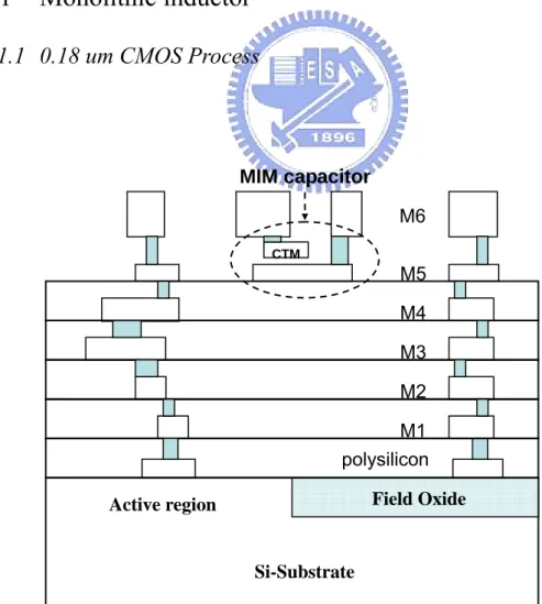
(16) Chapter 2 Basic concepts of the monolithic spiral inductors In this Chapter, some information of the commercial 0.18 um CMOS process used in this thesis is given in section 2.1. In addition, two typical layouts of monolithic inductors, asymmetric and symmetric patterns, are presented. They are very common in single-ended and differential excitation circuits, respectively. Section 2.2 summarizes the loss mechanisms of the on-chip inductors and section 2.3 analyzes the definition of the inductor quality factor.. 2.1. Monolithic inductor. 2.1.1 0.18 um CMOS Process. MIM capacitor M6 CTM. M5 M4 M3 M2 M1 polysilicon Field Oxide. Active region. Si-Substrate. Fig. 2.1. the cross section of the 0.18 um CMOS process 4.
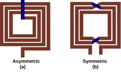
(17) As depicted in Fig. 2.1, the 0.18 process provides six metal layers (M1-M6) for interconnect and one polysilicon layer for the gate oxide of MOS transistor. Each of the first five metal layer has a thickness about 0.5 um and the top metal layer (M6) is thicker ALCu metal (physical thickness: 2 um) in order to lower the sheet resistance and to enhance the quality factor of on-chip spiral inductor. The dielectric constant, ε r between the metal layers is about 4. The Metal-Insulator-Metal (MIM) formed by the special metal layer (CTM) between the M6 and M5 has the unit capacitance of about 1 fF/um2. Besides, the resistivity of the Si-substrate is about 10 Ω-cm.. 2.1.2 Inductor Categories Fig. 2.2(a) (b) shows the two typical layout of the on-chip spiral inductor. In Fig. 2.2(a), the asymmetric inductor layout is shown and it consists of a rectangular spiral metal track wound on the silicon substrate, using one or two of the available standard metal layers. If the routing angle larger than 45-degree is allowed in the corresponding process, octagonal or circular spiral can be used. Octagonal or circular has lower series resistance than the traditional rectangular spiral with the aid of more smooth shape. Consequently, the better quality factor of octagonal or circular inductor. Asymmetric (a). Symmetric (b). Fig. 2.2 Typical asymmetric and symmetric inductor 5.
(18) can be achieved. On the other hand, the symmetric inductor pattern is shown in Fig.2.2 (b). Without being wound as a continuous metal spiral, the structure of the symmetric coil is connected to the inner turn by the different metal level. The symmetric inductors provide not only the area-saved solutions to the differential circuits but the higher quality factor, while it is differentially-driven, as shown in Fig. 2.3.[4]. Furthermore, the symmetric-shape layout is useful for the balanced circuit applications to show better common-mode noise rejection.. 2.2. Loss mechanism of the monolithic inductor In order to ease the latch-up issue in circuit designs, the CMOS process has been. a highly doped substrate. However, it leads to the more severe losses of monolithic inductors. The on-chip inductor losses can be categorized to two parts: conductor losses and substrate losses. The conductor losses contain the DC resistive losses and skin effect influence.. Quality factor (Q). 15. Qdifferential Qsingle-ended. 10. 5. 0. -5. 0. 2. 4. 6. 8. Frequency (GHz). Fig.2.3 Quality factors of symmetric inductors for single-ended /differential excitation 6. 10.
(19) Besides, the substrate losses include the substrate parasitic and eddy current effect. The following section will study these loss mechanisms related to the on-chip inductors.. 2.2.1 Conductor Loss 2.2.1.1 DC resistive loss The monolithic inductors are constructed by different layers of metal strip, typically aluminum. Even though the interconnect which is made of copper or gold is available, the finite conductivity of metal strip still causes resistive loss significantly. The resistance of a uniform slab of metal strip can be expressed as. ⎛ ρ ⎞⎛ l ⎞ R = ⎜ ⎟⎜ ⎟ ⎝ t ⎠⎝ w ⎠. (ohms ). ( 2.1). where ρ and t represent the resistivity and thickness of the metal strip. The area of the conductor is the same as the product of the conductor length (l) and width (w). The expression may be denoted as. ⎛l⎞ R = Rsh ⎜ ⎟ ⎝ w⎠. (ohms ). ( 2.2). where Rsh is the sheet resistance having units of Ω/square. From (2.2), the lower metal strip resistance of the inductor can be achieved with the reduced sheet resistance. In modern CMOS process, different layer metals have individual sheet resistance. Especially for RF application, the top metal layer is thicker in order to lower the sheet resistance and to enhance the on-chip inductor performance. For TSMC 0.18 um 1P6M standard process as example, the thickness of the sixth metal layer is 2um and that of other layers is 0.5um. Consequently, the sheet resistance of the top metal layer can be reduced to 0.018Ω but that of other layer metals is 0.078 Ω.. 7.
(20) From (2.1), another way to shrink the resistive loss is to make the width of metal track wider. Though it is an easy way to reduce the resistance without the process limitations, the too wider track width introduces large parasitic capacitance to enlarge the capacitive coupling to lossy substrate and to degrade self-resonant frequency. In general, in RF applications, the optimal width is ranged from 10um to 20um. Above all, it is still not possible to eliminate the resistive losses in standard process. Nevertheless, in case the wider and thicker metal track made of the high conductivity material like copper or gold is adopted, the issues of DC resistive losses can be alleviated. 2.2.1.2 Skin effect influence At low frequencies, the series resistance of the inductor is dominated by the DC resistive losses. At high frequencies, the current in the metal track tends to shift to the surface of the conductor, resulting in a non-uniform current distribution. This phenomenon is called skin effect. Thus, the series resistance of the inductor is no longer determined by the DC metal track resistance. The parameter of evaluating the skin effect is the skin depth which is defined as. δ=. ρ πµf. ( 2.3). where ρ is the resistivity of the metal strip, μ is the permeability of the metal material, and f is the operating frequency. The skin depth is also known as the figure of penetration since it describes the degree of the penetration by electric field and magnetic flux into the metal track at high frequency. The severity of the skin effect is judged by the ratio of the skin depth and the conductor thickness. Generally speaking, the skin effect is insignificant in case the skin depth is much larger than the conductor thickness.. 8.
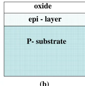
(21) 2.2.2 Substrate losses In this section, we will study the substrate losses, which include the substrate parasitic effects and the losses caused by eddy current. 2.2.2.1 The substrate of CMOS Process The cross section of the two typical substrates is shown in Fig. 2.4. The substrates include the lightly doped (1~30 Ω-cm) substrate shown in Fig. 2.4(a) and heavily doped substrate (10-20 mΩ-cm) shown in Fig. 2.4(b). The lightly doped substrate consists of a lightly doped bulk (P-bulk) and a thin layer of oxide. However, the high impedance substrate may cause latch-up problem in digital circuits. Thus, the typical epi substrate is composed of a lightly doped epitaxial layer grown on a degenerately doped. It is very low impedance but lossy substrate. 2.2.2.2 Substrate parasitic A main drawback of CMOS process is the conductive substrate. It degrades the performance of an on-chip inductor by three different coupling. In this section, we will study these coupling mechanisms individually. The first kind is the resistive coupling. For a doped semiconductor, the conductivity can be calculated as. σ = q • (nµn + pµ p ). ( 2.5). where q is the electric charge, n , p are the carrier concentration of the donor and acceptor, respectively. The μn and µp represent the mobility of the n type and p type carriers respectively. Due to the finite conductivity of the substrate, the electric. 9.
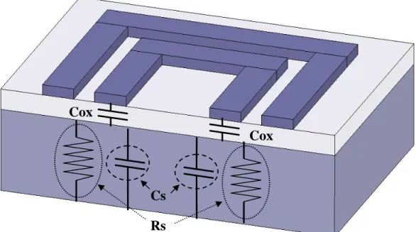
(22) oxide. oxide. epi - layer P- substrate. P- substrate. (a). (b). Fig. 2.4 Two types of CMOS substrate (a) P-substrate (b) P-epi layer on top of P-substrate. field leaking to the substrate produces the potential drop. As the operating frequency increases, the undesired energy dissipation in the substrate becomes more severe. Consequently, the loss reduction methodology like patterned ground shielding (PGS), as illustrated in Fig. 2.5, is proposed to block the electric field from entering silicon substrate. The second type is the capacitive coupling. For an on-chip inductor, the substrate parasitic has resistive and capacitive effect. The substrate effects can be modeled by a three-element network comprised of Cox, Rsi, and Csi, as shown in Fig. 2.6. The typical length of the on-chip inductor can be several hundred micro-meters. Therefore, large parasitic capacitances which consist of the capacitance between adjacent strips and strips to substrate are introduced. The capacitance between inductor and substrate can be calculated as : .. 10.
(23) metal-poly contact. poly. Fig. 2.5 Patterned Ground Shield (PGS). 11.
(24) Cox Cox. Cs Rs. Fig. 2.6 The substrate lumped circuit model. ε Cox = l • w • ox tox. ( 2.4). where єox and tox denote the effective dielectric constant and thickness of the oxide layer between the inductor and substrate. The l and w represent the length and width of the inductor. Apparently, the more turns the inductor is, the more significant capacitive parasitic effect will be. By virtue of the increased spacing to p substrate, using the higher level metal layer is effective to reduce the capacitance. As far as the penetration of the electric field into the semiconductor is concerned, the capacitance of the substrate can be neglected at low frequency but the high frequency capacitive effect is compatible to the resistive effect in the bulk. Both of the capacitive effects create the equivalent parallel capacitor that resonates with the inductor. The LC combination represents the upper useful frequency limit of the inductor. 12.
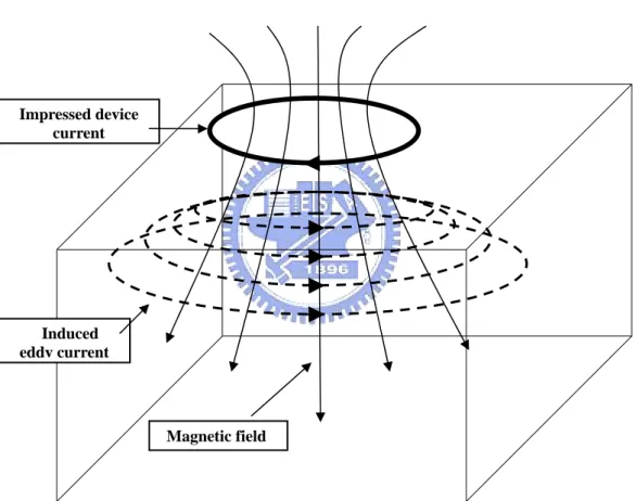
(25) Finally, the inductive coupling is also called “eddy currents”. That is, as the magnetic field penetrates into the conductive substrate, the opposite current will be introduced, as shown in Fig. 2.7. The induced current not only lowers the inductance but deteriorates the quality factor, especially at high frequency. It is noted that the magnetic coupling to the substrate can be neglected for lightly doped substrate since the substrate conductivity is typically low.. Impressed device current. Induced eddy current. Magnetic field. Fig. 2.7 Schematic representation of magnetically induced current. 2.3 Definition of Inductor Quality factor ………………….. The quality of an inductor is determined by its Q, quality factor. Several definitions are proposed to define the quality factor of an inductor. In these definitions, 13.
(26) the fundamental one is: Q = 2π •. energy stored energy loss in one oscillation cycle. ( 2.6). However, (2.6) also defines the Q of an LC tank. In a sense, (2.6) provides the physical insight but does not specify what stores or dissipates the energy. The main distinction is based on the form of energy storage. As far as an inductor is concerned, the energy stored in the magnetic field is of interest. Any energy stored in the electric field, due to the unavoidable parasitic effects in an on-chip inductor, is counterproductive. Thus, the energy stored can be interpreted as the difference between peak magnetic energy and electric energy. In contrast, for a LC tank, the energy stored is equal to the sum of the average electric and magnetic energy. Provided that an inductor is initially modeled as a simple parallel RLC circuit, it can be shown that [2]: Q = 2π •. peak magnetic energy − peak electric energy energy loss in one oscillation cycle. ( 2.7). 2 R ⎡ ⎛ω ⎞ ⎤ ⎢ ⎟ ⎥ = • 1− ⎜ ωL ⎢ ⎜⎝ ωo ⎟⎠ ⎥ ⎦ ⎣ Im(Z in ) = Re(Z in ). where R, L are the equivalent parallel resistance and inductance, respectively, and ω0 is the resonant frequency. Alternatively, the quality factor can be derived by the. ratio of imaginary and real part of the input impedance. The expression is valid for two different excitations. If the inductor is single-ended driven, one terminal of the spiral inductor is excited by the ac source while the other terminal is connected to the common reference port (e.g. the supply voltage or ground). The corresponding input impedance is the impedance seen at one terminal as the other terminal is connected to the ground. On the other hand, for the differential-driven (i.e., voltages and currents at 14.
(27) two terminals are 1800 out of phase), the differential input impedance is the impedance seen between two terminals. Moreover, Inductor quality factor is a frequency-dependent function and it is vital to introduce some indexes used in the thesis. An inductor is at self-resonance as the peak magnetic and electric energy is equal. Thus, the quality factor will vanish to zero at the self-resonant frequency (FSR), as shown in Fig. 2.8. Above the resonant frequency, no energy is available from an inductor to the external circuit. Besides, the frequency where the maximal quality factor (QMAX )is attained is called as fQMAX... 10. QMAX 8 6. Q. 4 2. 0. 0 -2 -4 0. fQmax3. fSR 9 freq, GHz Frequency 6. 12. Fig. 2.8 The quality factor of monolithic inductor. 15. 15.
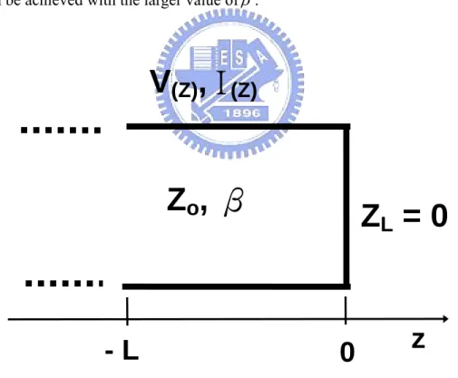
(28) CHAPTER 3 Theoretical analysis and structure of the miniature inductor In this chapter, the proposed miniature inductors utilizing a high slow-wave-factor coplanar stripline (HS-CPS) are presented. The design flow of the proposed miniature inductors, which include the two patterns, shifted and folded inductors, is demonstrated. Some design equations and considerations are shown from the transmission line theory. They provide useful design guidelines to optimize the proposed inductor. Finally, the simulation results are shown and the effects of the metal shunting, the arrangement of the MIM capacitors, different phase constant, and folded structures are also studied.. 3.1 Theoretical Analysis and Design Considerations Fig. 3.1 shows the common single stub matching with a short circuit terminated transmission as the inductive element. The input impedance of a lossy line of length l can be expressed:. Z in = Z o ⋅ tanh (γ l ) = (R + jX ) ⋅ tanh ((α + β j )l ). (3-1). The effective inductance and quality factor below the first resonant frequency is defined respectively by: Leff =. imag ( Z in ) 2πf. =. imag ( Z in ) real ( Z in ). Q. (3-2). (3-3). 16.
(29) From (3-1), (3-2) and (3-3), we have. Leff =. Q. R tan (βl ). (3-4). ω. sin 2 β l X + sinh 2 α l R = X sin 2 β l 1− R sinh 2αl. (3-5). According to the transmission line theory, the propagation constant of a lossless transmission line is given as β = ω LC. where L and C are the distributed. inductance and capacitance per unit length along the transmission line. Eq. (3-4) shows that in case the β l product keeps constant, the shorter length of transmission line can be achieved with the larger value of β .. V(Z), I (Z). Zo, β. -L. ZL = 0. 0. z. Fig. 3.1 Transmission line with short circuit terminal as the inductive element. Coplanar Stripline (CPS) is an attractive uniplanar transmission line for on-chip interconnects, as shown in Fig.3.2 (a), (b). As compared to the conventional 17.
(30) microstrip structure, CPS is insensitive to the properties of substrate and is simple implementation of open- or short- ended strips. Especially for standard CMOS process, its balanced structure is useful for the ease of substrate loss. Furthermore, HS-CPS is proposed to decrease the occupied area and total attenuation as compared to the conventional coplanar stripline [5]. The structure of HS-CPS is depicted in Fig. 3.2 (a), (c). With the aid of enhanced β in HS-CPS structure, the overall length of inductor can be shorter, as above elucidated. According to (3-5), the Q factor can be optimized with the lower α and the appropriate βl product. Energy dissipation mainly arises from the lossy Si substrate and the resistivity due to non-ideal conductors. Not only the nature of differentially excitation, but the additional MIM capacitors alleviate the energy coupling to the substrate. That is to say, electric field is largely confined near the region of MIM capacitors. Only a fraction of electric field penetrates into the silicon. Thus, the issue of substrate loss is insignificant. As to the metal loss, the Metal 6 and Metal 5 are shunted to obtain the lower line resistance. On the other hand, from (3-5), it can be observed that the sinusoid function included in Q expression approaches the maximum as the product of βl goes to 45o. It is favorable to optimize Q at a given frequency by tuning the βl product up to 40o~45o.. 3.2 Proposed Miniature Inductor Structure. The design flow of the proposed miniature inductors, which contains two patterns, is illustrated in Fig.3.3. Since the length of the proposed miniature inductor will be as long as several hundred micrometers, the inductors are folded to save the. 18.
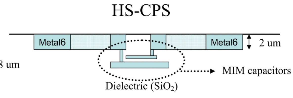
(31) CPS. HS-CPS (a). CPS Metal6. 8 um. 450 um. Metal6. Dielectric (SiO2). Si Substrate. (b). 19. 2 um.
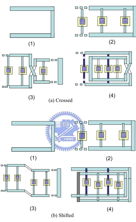
(32) HS-CPS Metal6. Metal6. 8 um. 2 um. MIM capacitors Dielectric (SiO2). 450 um. Si Substrate. (c) Fig. 3.2 Monolithic coplanar stripline (a) Top view of the conventional CPS and HS-CPS. Cross-sectional view of (b) the conventional CPS and (c) HS-CPS. occupied area. Thanks to the mutual coupling between two paralleled HS-CPS, the distributed inductance per unit length (L) and phase constant (β) are enhanced, and it leads to more length reduction. The crossed pattern consists of the HS-CPS which is crossed and folded in the center as shown in Fig.3.3 (a)-(3), (4) respectively. Besides, the other inductor pattern is the shifted of Fig.3.3 (b).The conventional CPS is shifted and folded orderly as the depiction in Fig.3.3 (b)-(3), (4). As compared with the crossed pattern, the shifted can achieve the higher quality factor and self-resonant frequency due to the removal of the underpass between two metal layers.. 20.
(33) (2). (1). (3). (a) Crossed. (4). (1). (2). (3). (4) (b) Shifted. Fig. 3.3.Design flow of miniature inductor patterns. 21.
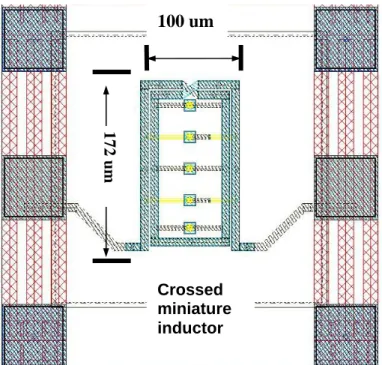
(34) 3.3 Inductor design In this section, the simulation results of three inductor configurations, the symmetric spiral, the crossed miniature, and the shifted miniature inductors, are shown for comparisons. A commercially available, 2.5 D EM simulation software, ADS Momentum, is used to extract the S-parameters and corresponding electrical parameters in all the patterns.. 3.3.1 Simulation results In order to quantify the improvement in area reduction, two inductor patterns, the crossed and the shifted miniature inductor, (with nominal inductance 1nH) have been designed and implemented in UMC 0.18um CMOS technology. The total length of these inductors is expected to be shorter than 200 um (folded). Furthermore, the maximal quality factor is designed near 10 G-Hz to manifest the facility in Q tuning, as mentioned in section 3.1 From (3-4), the propagation constant β and the real part characteristic impedance R of the miniature inductor are derived as 1.8 (rad/mm) and 75 Ω for the required inductance (1nH) and βl product. The HS-CPS line consists of 8um-wide traces separated by 75um gap. Five MIM capacitors, each of 16 fF, are needed to be distributed in the CPS to meet the sufficient β. The total length of the miniature inductors is 172 um and the spacing between MIM capacitors, 64 um, can be decided by the quotient (2*172 /5). The design flow of the proposed miniature inductor is shown in Fig. 3.4. Fig. 3.5 shows the layout of one spiral and two proposed miniature inductor. The. 22.
(35) Start. Decide a configuration width. Choose a strip width. Add MIM capacitors between CPS. Remove a few MIM capacitors Zo < 75. Zo > 75. Zo= 75 Ω. Derive the required length for 1nH. Acceptable overall length. No. Yes Proper quality factor Q. Q < needed. END. Fig. 3.4 The design flowchart of the proposed miniature inductor. 23.
(36) 115um. 172 um Spiral symmetric inductor. (a). 100 um. 172 um Shifted miniature inductor. (b). 24.
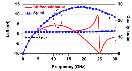
(37) 100 um. 172 um Crossed miniature inductor. (c) Fig. 3.5 Layout of (a) the spiral symmetric inductor, (b) the crossed and (c) the shifted miniature inductor sizes of the spiral inductor and miniature inductors are 172µm by 115µm and, 172µm by 100µm. respectively. In the case for the conventional spiral inductor, the. spacing(s) between conductors is 2 um, and the strip width is similarly chosen as 8 um for comparison. In this example, the miniature inductors uses only 87 % of the area to achieve the same inductance as the spiral inductor and the peak Q of the miniature inductor occurs approximately near 10GHz, as shown in Fig. 3.6. However, the miniature inductor decreases self-resonance frequency to 25.5 GHz with 18.6 % degradation of the quality factor, from 22.8 to 17.2. Moreover, Fig. 3.7 displays the effective inductance and quality factor of the crossed and the shifted miniature inductors with the same area. The shifted miniature inductor increases the quality factor by 6 %, from 16.2 to 17.4, without any degradation of self-resonance frequency. Note that the improvement in Q benefits. 25.
(38) 15. 20. 5 0. 10. -5. Quality factor. 10 Leff (nH). 30. Shifted miniature Spiral. 0. -10 0. 5. 10. 15. 20. 25. 30. Frequency (GHz). Fig. 3.6 Effective inductance (Leff) and quality factors (Q) of the spiral and the shifted miniature inductors. 15. 20. Leff (nH). 15. 5 10 0 5. Shifted miniature crossed miniature. -5 -10. Quality factor. 10. 0 0. 5. 10. 15. 20. 25. 30. Frequency (GHz). Fig. 3.7 Effective inductances (Leff) and quality factors of the crossed and shifted miniature inductors.. 26.
(39) Table 3.1 Inductor Comparison Symmetric spiral. Shifted Miniature. Crossed Miniature. Qmax. 28.5 @ 19GHz. 17.4 @ 10 GHz. 16.2 @ 13GHz. Self-resonance Frequency. >30GHz. 25.5 GHz. 26GHz. 115*172. 100*172. 100*172. 1. 0.87. 0.87. Area (um2) Area ratio*. * Area ratio :. Area(Symmetric ; Shifted ; Crossed ) Area(Symmetric ). from the removed underpass of the shifted miniature inductor, as demonstrated previously. The performances of the symmetric spiral inductor and the miniature inductors are summarized and compared in Table 3.1. The reduction in Q is for the reason that the energy is saved in the MIM capacitors in the form of electric energy as the phase constant β is enlarged by the increased capacitance per unit length along the transmission line. The quality factor of an inductor is defined as [2]:. Qinductor =. peak magnetic energy − peak electric energy energy loss in one oscillatio n cycle. Namely, it will be counterproductive that any energy is stored in the inductor’s electric field.. 27.
(40) 3.3.2 The effect of the metal layer shunting As shown in equation (2.1) of section 2.2, the DC series resistance can be reduced by increasing the effective thickness of the metal strip. Shunting several metal layers is a simple solution in the commercial multilevel interconnects technology without any process modifications. However, shunting of metal layers will also reduce the oxide thickness between inductor and silicon substrate and the Cox, as shown in Fig.2.6, becomes larger. It degrades the quality factor at low frequency compared to a single-layer inductor built by using only the top metal. Therefore, the tradeoff between reducing the series resistance and minimizing the Cox should be concerned. In this thesis, the inductors of a single metal layer (M6), shunted M6/M5 layers, and shunted M6/M5/M4 layers are investigated (with nominal inductance 1nH). The quality factor of the three cases is illustrated in Fig. 3.8. It is found that the maximal quality factor can be achieved for the M6/M5 coil compared to the M6 and M6/M5/M4 inductors, especially at our design frequency (10GHz), without any degradation of self-resonant frequency. Since the M6/M5 inductor has the lowest real part of the input impedance, as depicted in Fig.3.9, the shunting of M6/M5 is the optimal choice for our design. Besides, according to the maximal quality factor of three cases, layer shunting is beneficial at lower frequencies (i.e. lower than 10 GHz in this case) where coil losses dominate but are less advantageous at higher frequencies where substrate losses are significant. The observation is also consistent with the published early work [3].. 28.
(41) Quality factor (Q). 25 M6 M6M5. 20. M6M5M4. 15 10 5 0. 0. 5. 10. 15. 20. 25. Frequency (GHz) Fig. 3.8 Quality factor comparison of shunting of three (M6/M5/M4), two (M6/M5), and the top metal layer (M6). real(Zin) (Ohms). 25 M6 M6M5. 20. M6M5M4. 15 10 5 0 0. 5. 10. 15. 20. 25. Frequency (GHz) Fig. 3.9 Quality factor comparison of shunting of three (M6/M5/M4), two (M6/M5), and the top metal layer (M6). 29.
(42) 3.3.3 The effect of the arrangement of MIM capacitors In order to find out the effect of the arrangement of MIM capacitors, the performance of two miniature inductors containing eight 3.16x3.16um2 and two 6.32x6.32 um2 MIM capacitors respectively, as shown in Fig.3.10, are compared with the aforementioned miniature inductor including five 16x16um2 MIM capacitors. That is, the total inserted capacitance remains the same but the number of MIM capacitors is different. Fig.3.11 and Fig.3.12 show the simulation results of the effective inductance and quality factor of three miniature inductors individually. It is found that there is no significant difference between three miniature inductors. In other words, the arrangement of MIM capacitors does not matter.. 30.
(43) 100 um. 6.32 um 172 um. 8 um (a) 100 um. 3.16 um 172 um. 8 um. (b). Fig. 3.10 The miniature inductors of (a) two 6.32x6.32 um2 MIM capacitors and (b) eight 3.16x3.16 um2 MIM capacitors 31.
(44) Leff (nH). 5 4. 2 cell 5 cell. 3. 8 cell. 2 1 0. 0. 5. 10. 15. 20. 25. Frequency (GHz) Fig. 3.11 Effective inductance comparison of 2 cell, 5 cell, and 8 cell MIM capacitors distribution. 25 2 cell 5 cell. Quality factor. 20. 8 cell. 15 10 5 0 0. 5. 10. 15. 20. Frequency (GHz) Fig. 3.12 Quality factor comparison of 2 cell, 5 cell, and 8 cell MIM capacitors distribution. 32. 25.
(45) 3.3.4 The performance of the inductor consists of different phase constant (β) HS-CPS In order to evaluate the relationship between phase constant (β) and inductor parameters, two analyses are conducted. First, this analysis is under the constraint that the inductor is made of constant characteristic impedance transmission line. The strip width of the HS-CPS can be reduced and the capacitance of MIM capacitors can be inserted for higher inductance and capacitance per unit length along the HS-CPS. Therefore, the higher phase constant (β) and shorter required length can be obtained. However, as the strip width shrinks, the series resistance of the HS-CPS would rise up leading to the degraded quality factor. That is, the trade-off between phase constant and series resistance should be made. Three HS-CPS structures of different strip width, 3μm, 8μm, and 13μm, as depicted in Fig.3.13, are investigated. Through the simulator, ADS momentum, MIM capacitors of different capacitance, 21.6fF, 16fF, and 13.1 fF are used in the three HS-CPS structures respectively to maintain the same characteristic impedance, 70 Ω at 10 GHz. Phase constant (β), quality factor of the inductors, and imaginary part of characteristic impedance, overall attenuation, i.e. the product of attenuation constant and inductor length, are given in Fig.3.14 and Fig. 3.15 (a), (b), (c). The corresponding phase constant at 10 GHz of HS-CPS of three strip width is 1.63, 1.38, and 1.14, respectively. According to equation (3.4), the inductors with effective inductance 1nH are designed and overall length of three configurations, 0.449 mm, 0.558 mm, and 0.643 mm, is required. As shown in Fig.3.14 and 3.15(a), the highest phase constant is obtained by the HS-CPS of 3µm strip width with value about 1.63 but the quality factor is the lowest one due to the increased series resistance of the narrowest strip width. The HS-CPS of 33.
(46) 13µm strip width has the least phase constant but the most superior quality factor. According to (3.5), the imaginary part of characteristic impedance of the HS-CPS of 13µm strip width reaches the highest value with 0.858 and compensates the significant overall attenuation, as given in Fig. 3.15(b), (c), Although the HS-CPS of 8µm strip width shows the least overall attenuation, the imaginary part of characteristic impedance is not large enough to maximize the quality factor. Second, the inductors are formed by the HS-CPS with different characteristic impedance and phase constant. Three HS-CPS structures of different MIM capacitors spacing, 32 μm, 64 μm, and 128 μm, depicted in Fig.3.16, are investigated. The strip width and spacing between strips is fixed at 8μm and 84 μm. The MIM capacitors are inserted for higher capacitance per unit length along the HS-CPS. Therefore, the higher phase constant (β) and shorter required length can be obtained. Through the simulator, ADS momentum, the phase constant (β), real part of characteristic impedance, quality factor is given in Fig.3.17 and Fig. 3.18(a), (b). As shown in Fig.3.17 and Fig. 3.18(a), the corresponding phase constant of three HS-CPS configurations is 1.78, 1.31, and 1.14, respectively. According to equation (3.4), the inductors with effective inductance 1nH are designed and the required length is 0.497 mm, 0.558 mm, and 0.6 mm, separately. The highest phase constant is obtained by the HS-CPS of 32 µm MIM capacitors spacing with value about 1.78 but the real part of characteristic impedance is the lowest one due to the increased distributed capacitance. The quality factor of the HS-CPS of 1.14 phase constant reaches the highest value about 16.9, as shown in Fig. 3.18(b). Above all, the trade-off between phase constant and quality factor (Q) should be made. By shrinking the strip width and inserting the MIM capacitors, the higher phase constant and size reduction will be available but the quality factor is degraded 34.
(47) simultaneously.. 3.3.5 The influence of folded HS-CPS In this section, the effect of the folded HS-CPS is studied. Two folded structures, crossed and shifted patterns, are proposed in this thesis and the crossed configuration is taken as an instance. Two HS-CPS structures, unfolded and folded, depicted in Fig.3.19 (a), (b), are analyzed. Both configurations have the same strip width, 8um, and MIM capacitors distribution (16 fF per 64μm). By 2.5D simulator, ADS momentum, distributed inductance (L), capacitance (C), resistance (R), and conductance (G) per mm of the two HS-CPS structures are given in Fig. 3.20(a), (b), (c), (d). According to Fig 3.20(a), (b), the folded structure has higher inductance per mm than unfolded one since magnetic flux of the folded structure is enhanced due to positive mutual inductive coupling. However, the folded structure would also show higher distributed capacitance due to the decreased spacing between strips from 84μm to 64μm and the capacitive effect of two adjacent HS-CPS. Besides, as depicted in Fig 3.20(c), (d), since the current distribution is disturbed and the induced eddy current in the inner HS-CPS, the series resistance per mm in the folded formation is increased. In addition, the folded structure shows better immunity to substrate due to the lower distributed conductance. From viewpoints of wave characteristics, the behavior of transmission line can be sketched with propagation constant (γ) and characteristic impedance (Zo). Real and imaginary part of propagation constant and characteristic impedance of the two HS-CPS structures is illustrated in Fig. 3-21(a),(b), and Fig. 3-22(a),(b). According to [6], the two HS-CPS structures satisfy the low-loss conditions and the propagation constant and characteristics impedance can be expressed as:. 35.
(48) γ = α + jβ where α ≅. 1⎛ C L⎞ ⎜R ⎟ + G 2 ⎜⎝ L C ⎟⎠. (3.6). β ≅ ω LC Z o = Ro + jX o where Ro ≅ L C Xo ≅ −. (3.7). L 1 ⎛R G⎞ ⎜ − ⎟ C 2ω ⎝ L C ⎠. where R, L, C, G are the distributed transmission line parameters. According to (3.6) and (3.7) and the observation on transmission line parameters as aforementioned, the trend and variation of propagation constant and characteristic impedance of unfolded and folded patterns can be explained sufficiently.. 36.
(49) 0.449 mm 3 um 100 um. 4.65 um. (a). 0.558 mm 8 um 100 um. 4.0 um. (b). 0.643 mm 13 um 100 um. 3.62 um. (c). Fig. 3.13 Three HS-CPS structures of (a) 3 μm strip width (b) 8 μm strip width (a) 13 μm strip width. 37.
(50) 4. Beta(rad/mm). width=13 um. width=8 um. 3. width=3 um. 2 1 0 0. 5. 10. 15. 20. 25. Frequency (GHz) Fig. 3.14 phase constant of the HS-CPS structures with different strip width. 20. Quality factor. β=1.14. β=1.31 β=1.63. 15 10 5 0 0. 5. 10 15 Frequency (GHz) (a). 38. 20. 25.
(51) Frequency (GHz) 0. 5. 10. 15. 20. 25. Imag(Zo) (ohms). 5. 0. β=1.14. -5. β=1.31 β=1.63 -10 (b). alpha*l (Neper). 0.060 0.045 0.030 β=1.14 β=1.31 β=1.63. 0.015 0.000 0. 5. 10. 15. 20. 25. Frequency (GHz) (c) Fig. 3.15 (a) quality factor, (b) imaginary part of characteristic impedance (c) overall attenuation (Neper) of the HS-CPS structures with different phase constant.. 39.
(52) 0.497 mm 8 um 100 um. 4.07 um. 32 um. (a). 0.558 mm 8 um 4 um. 100 um. 64 um. (b). 0.6 mm 8 um 100 um. 3.87 um. 128 um. (c). Fig. 3.16 Three HS-CPS structures of different spacing between MIM capacitors (a) per 32μm (b) per 64 μm (a) per 128 μm. 40.
(53) 5 spacing=128 um spacing=64 um spacing=32 um. Beta(rad/mm). 4 3 2 1 0 0. 5. 10. 15. 20. 25. Frequency (GHz) Fig. 3.17 phase constant of the HS-CPS structures with different spacing between MIM capacitors. 41.
(54) 100. real(zo) (ohms). 80 60 40 β=1.14. 20. β=1.31 β=1.78. 0 0. 5. 10. 15. 20. 25. Frequency (GHz) (a). 20. Quality factor. β=1.14 β=1.31. 15. β=1.78. 10 5 0 0. 5. 10 15 Frequency (GHz). 20. 25. (b) Fig. 3.18 (a) real part of characteristic impedance (b) quality factor for the 1nH inductor of the HS-CPS structures with different phase constant. 42.
(55) 344 um 8 um. 100 um. 4 um. (a). 172 um 8 um. 100 um 4 um. (b). Fig. 3.19 (a) unfolded (b) folded HS-CPS structures. 43.
(56) 3.0. L (nH/mm). 2.5 2.0 1.5 1.0. unfolded folded. 0.5 0.0 0. 5. 10. 15. 20. Frequency (GHz) (a). 500. C (fF/mm). 400 300 200 unfolded folded. 100 0 0. 5. 10 15 Frequency (GHz) (b). 44. 20.
(57) 10. R (ohms/mm). 8 6 4 2. unfolded folded. 0 0. 5. 10. 15. 20. Frequency (GHz) (c). 1500 unfolded folded. G (uS / mm). 1200 900 600 300 0 0. 5. 10 15 Frequency (GHz). 20. (d) Fig. 3.20 (a) Inductance (b) capacitance (c) resistance (d) conductance per mm of the unfolded and folded HS-CPS. 45.
(58) alpha(Neper/mm). 0.09 0.06 unfolded folded. 0.03 0.00 0. 5. 10. 15. 20. Frequency (GHz) (a). 5 unfolded folded. Beta(rad/mm). 4 3 2 1 0 0. 5. 10. 15. 20. Frequency (GHz) (b) Fig. 3.21 (a) real part (attenuation constant) (b) imaginary part (phase constant) of propagation constant of two HS-CPS structures. 46.
(59) real(zo) (ohms). 80 70 60 unfolded folded. 50 40 0. 5. 10. 15. 20. Frequency (GHz) (a). Imag(Zo) (ohms). 3 0 -3 -6. unfolded folded. -9. -12 0. 5 10 15 Frequency (GHz). 20. (b). Fig. 3.22 (a) real part (b) imaginary part of characteristic impedance of two HS-CPS structures. 47.
(60) CHAPTER 4 Experimental results and application of the miniature inductor In this chapter, the experimental results of the proposed miniature inductors which are fabricated in UMC 0.18 technology are presented. The measurement test structure and the de-embedding procedures used to extract the experimental results are described as well. Besides, the 5-GHz CMOS LC-VCO has also been fabricated in TSMC 0.18 technology to verify the functions of the miniature inductors.. 4.1 Measurement results and discussions 4.1.1 Measurement setup Figure 4.1 shows the measurement setup. The raw S-parameters of the device under test (DUT) were measured by HP 8510 Network analyzer and Cascade Microtech probe station. Measuring with the RF probes, as illustrated in Fig.4.2, GSG-pads consist of three 80μm by 80μm square pads where the DUT is the proposed miniature inductor in this thesis. The spacing between two pads from center to center is 150 μm.. 4.1.2 De-embedding method Since the parasitic effects of the GSG pads should be removed to acquire the intrinsic S-parameters of the DUT, a process called “de-embedding” should be performed for a complete two port calibration. A general procedure of de-embedding consists of open circuit, short circuit, and through circuit de-embedding (OSTD) and is used in this measurement. The equivalent circuit model of the parasitics of the pad 48.
(61) HP 8510 Network Analyzer. Coplanar GSG Probe. DUT. port1. port2. Fig. 4.1 Experimental set up for measurement. RF Probe. G. G. S. S. G. G. Fig. 4.2 Coplanar GSG RF probes and the DUT. 49. RF Probe.
(62) and interconnect (Zi ,yp,Zl) and DUT is depicted in Fig. 4.3(a). After the input impedances of the open (Zin, open), short (Zin,short), and through (Zin,through) pads, as depicted in Fig. 4.3 (b) are measured, the three parasitics (Zi ,yp,Zl) can be extracted from the following equations:. Z i = Z in ,short yp =. (Z. in ,open. (4.1) 1 − Z in ,short ). (4.2). ⎛ ⎞ ⎜ ⎟ 1⎜ 1 1 ⎟ − Zl = ⎟ 1 1 2⎜ − yp yp + ⎜ ⎟ Z in ,s + 50 ⎠ ⎝ Z in ,through − Z in ,short. (4.3). ⎡ A B⎤ The ABCD matrix of the DUT, ⎢ , can be derived: ⎥ C D ⎣ ⎦ DUT ⎡A B⎤ ⎡1 Z i ⎤ ⎡ 1 =⎢ ⎢C D ⎥ ⎥⎢ ⎣ ⎦ total ⎣0 1 ⎦ ⎢⎣ y p. 0 ⎤ ⎡1 Z l ⎤ ⎡ A B ⎤ ⎡1 Z l ⎤ ⎡ 1 ⎥ ⎢ ⎥ ⎢ ⎥ ⎢0 1 ⎥ ⎢ y 1⎥⎦ ⎣0 1 ⎦ ⎣C D ⎦ ⎦ ⎢⎣ p DUT ⎣ −1. ⎡ A B⎤ ⎡1 Z l ⎤ ⎡ 1 ⇒⎢ =⎢ ⎥ ⎥ ⎢ ⎣C D ⎦ DUT ⎣0 1 ⎦ ⎣ y p. −1. −1. 0 ⎤ ⎡1 Z i ⎤ 1⎥⎥⎦ ⎢⎣0 1 ⎥⎦ −1. 0⎤ ⎡1 Z i ⎤ ⎡ A B ⎤ ⎡1 Z i ⎤ ⎡ 1 1⎥⎦ ⎢⎣0 1 ⎥⎦ ⎢⎣C D ⎥⎦ total ⎢⎣0 1 ⎥⎦ ⎢⎣ y p. Therefore, the S-parameters of the DUT, [S ]DUT , can be derived from:. [S ]DUT. ⎡S = ⎢ 11 ⎣ S 21. S12 ⎤ where S 21 ⎥⎦ DUT. S11 =. A + B 50 − C * 50 − D A + B 50 + C * 50 + D. ,. S12 =. 2 * ( AD − BC ) A + B 50 + C * 50 + D. S 21 =. 2 A + B 50 + C * 50 + D. ,. S 22 =. − A + B 50 − C * 50 + D A + B 50 + C * 50 + D. 50. −1. 0⎤ ⎡1 Z i ⎤ 1⎥⎦ ⎢⎣0 1 ⎥⎦. −1.
(63) S. S. DUT. ZL. Zi. ZL. Zi yp. yp. G. G. (a). Zin,short. Zin,open. S. S Zi. Zi yp. G. G. Zen, through S. S Z. Zi. Z. Zi. yp. yp. G. G (b). Fig. 4.3 (a) The equivalent circuit model of the DUT and the parasitics of the pads and interconnects (b) the input impedances 51.
(64) Then, we can derive the differential one port S parameters (Sd) from the single-ended S-parameter ( [S ]DUT ) [4]: S + S 22 − S12 − S 21 S d = 11 2 and the corresponding input impedance for differential excitation ⎛ 1 + Sd Z d = 2 Z o ⎜⎜ ⎝ 1 − Sd. ⎞ ⎟⎟ ⎠. (4.4). As mentioned in section 2.3, the effective inductance and quality factor can be written in terms of Zd : Leff = Q=. 4.1.3. imag (Z d ) (2 * pi * freq ). imag (Z d ) real (Z d ). Measurement results and discussions. The micrograph of test chip is shown in Fig.4.4. The upper and lower hand corner. Fig. 4.4 Micrograph of test chip. 52.
(65) pattern is crossed and shifted inductor, respectively. The upper and lower right hand corner is de-embedding pattern and conventional spiral inductor. The measurement results of three patterns together with simulation results are shown in Fig. 4.5, 4.6, and 4.7 and are summarized in Table 4.1. The solid line shows the measured data and the curve with square marker presents the simulation data. For effective inductance, good agreement with the simulation is shown with only minus 0.06 nH that is nearly 6 % deviation, maximally for all three inductor patterns and the effective inductance is about 0.92 nH at 10 GHz. Moreover, the self resonant frequency of the crossed and shifted inductor is 27.5 and 26.2 GHz, respectively. The increment about 1~1.5 GHz is mainly due to the slight deviation of the inductance. The resonant frequency of spiral inductor is more than 40 GHz as expected. As shown in Fig.4.5 (b) and Fig.4.6 (b), the measured Q of the crossed, shifted and spiral inductor is 13.9, 13.3, and 16.9 at 10 GHz, individually. The measured Qmax is near 10GHz as we artificially designed. Besides, the measured Q of spiral inductor is 15.3 at 10 GHz. However, there is a discrepancy of measured and simulated Q observed during 5~15 GHz. Since there is no significant difference between measurement and simulation results in inductance, the degradation in quality factor implies the raising of input impedance according to the definition of quality factor. As shown in Table 4.2, the increment of input impedance ranges from 0.33 to 0.8 ohms. Even though the order of increment is lower than 1 ohm, that still puts the dramatic influence on quality factor especially near its maximal. This addition might source from the contact resistance during on-wafer probing and insufficient-deembedding of thru parasitics. First, the typical contact resistance of a probe is 0.03~0.15 ohms [7] in case the touchdown is regular and repeatable. As probing is not so perfect, the extra. 53.
(66) contact resistance is generated and the decrease of quality factor follows. Compared with the larger inductance measurement, the smaller inductor in our case is more sensitive to the increased contact resistance. Next, as depicted in Fig. 4.8 , the resistance of thru parasitics might be lower than usual during 5 ~ 15 GHz and it results in the insufficient deembeding for the interconnect between pad and inductor. This also raises the measured resistance of the inductor.. 54.
(67) 10 Measurement. Leff (nH). 5. Simulation. 0 -5 -10. 0. 5. 10. 15. 20. 25. 30. Frequency (GHz) (a). 25 Measurement. Quality factor. 20. Simulation. 15 10 5 0 0. 5. 10. 15. 20. 25. Frequency (GHz) (b) Fig. 4.5 (a) Effective inductance (b) Quality factor of the proposed crossed miniature inductor. 55. 30.
(68) 10 Measurement Simulation. Leff (nH). 5 0 -5 -10. 0. 5. 10. 15. 20. 25. 30. Frequency (GHz) (a). 25 Measurement Simulation. Quality factor. 20 15 10 5 0. 0. 5. 10. 15. 20. 25. Frequency (GHz) (b) Fig. 4.6 (a) Effective inductance (b) Quality factor of the proposed shifted miniature inductor. 56. 30.
(69) 3 Measurement. Leff (nH). Simulation. 2. 1. 0 0. 10. 20. 30. 40. Frequency (GHz) (a). 35 Measurement. Quality factor. 30. Simulation. 25 20 15 10 5 0. 0. 10. 20. 30. Frequency (GHz) (b) Fig. 4.7 (a) Effective inductance (b) Quality factor of the conventional spiral inductor. 57. 40.
(70) Table 4.1 Summary of simulated and measured results of proposed miniature inductor and conventional spiral inductor Shiftind Crossind Spiralind (mea. / sim. ) (mea. / sim. ) (mea. / sim. ) Leff [nH] 0.93 0.99 0.92 0.97 0.91 0.96 Q. 13.3. 17.3. 13.9. 15.9. 16.9. 21.6. FSR [GHz]. 26.2. 25. 27.5. 26. >40G. >40G. Area(um2). 172*100. 172*100. -13 %. -13 %. A.R.. * A.R. =. 172*115. Area dut −1 Area spiral. Table 4.2 The measurement and simulation results of input impedance for three inductor patterns Shiftind ( mea. / sim. ) 13.3 17.3. Q Real(Zin). 4.4. Offset. Crossind ( mea. / sim. ) 13.9 15.9. 3.6. 4.16. +0.8. 3.83. Spiralind (mea. / sim. ) 16.9 21.6 3.38. +0.33. 2.79 +0.59. Through resistance (ohm). * Offset = real (Z in )mea. − real (Z in )sim. 1.5. 1.0. 0.5. 0.0. 0. 5. 10. 15. 20. 25. Frequency (GHz) Fig. 4.8 the measured resistance of through parasitics. 58. 30.
(71) 4.2 Circuit application Differentially driven symmetric inductor is widely used in balance circuit applications, such as VCO. The 5-GHz LC-VCO utilizing the proposed miniature inductor is implemented in TSMC 0.18μm technology.. 4.2.1. Design Flow and Simulation Results. The schematic of oscillator circuit is depicted Fig. 4.9, which uses a complementary structure to omit a connection to the common-mode point of the inductor. It is possible to use only one symmetric inductor in this design. Besides, the crossed coupled pair formed by NMOS and PMOS transistors is used to generate a negative conductance and the output buffer is realized by a common-drain PMOS transistor. Providing the sufficient bias current for VCO, the current mirror comprises an N+ diffusion resistor (R2) and two PMOS transistors, which have larger channel width to suppress the thermal noise. The tank of LC-VCO consists of the proposed miniature inductor and group 3(G3) varactor available in TSMC process. The tunable capacitances range from 0.4pF to 1.8pF with different applied voltage at 5GHz, as shown in Fig.4.10. Accordingly, the single-turn inductor with the nominal inductance 0.7nH is needed to form a 5GHz resonator. Just as the design flow illustrated in Fig.3.4, there are several steps to design a miniature inductor. First, since the Q of resonator has significant effects on phase noise in a LC-tank VCO, the wider strip width (25μm) is adopted to improve the quality factor of the miniature inductor. Next, in order to satisfy the βl product (17o)and the expected length (300 μm), the required phase constant β and real part characteristic impedance R is 1.54 (rad/mm) and 27.9 ohms, respectively. Then, three MIM capacitors, each of 21.5 fF, are uniformly distributed. 59.
(72) Vdd. M5. M6 R2 M3. M4. Bias-T. Bias-T. M3. M7. M8 C1. C2 R1. M1. M2. Vcontrol. Fig. 4.9 Schematic of 5GHz LC-VCO circuit utilizing the proposed miniature inductor. 60.
(73) 25 20. 1.5. 15 1.0 10 0.5. 5. 0.0. Quality factor at 5 GHz. C_varactor (pF). 2.0. 0 -2. -1. 0. 1. 2. Varactor Bias Voltage. Fig.4.10 C-V and Q-V of the G3 varactor at 5 GHz within the CPS and the distance between two MIM capacitors can be estimated by the quotient of (300/3). Finally, finely tuning the spacing between the CPS is to have the sufficient effective inductance. The dimensions, effective inductance, and quality factor of the single-turn inductor and miniature inductor, for the same inductance, are shown at Fig.4.11(a),(b),and (c) individually and are summarized in Table 4.3. As expected, the proposed miniature inductor uses 90% of the area of the single turn inductor for the same inductance. Simulation results of phase noise and tuning range of the voltage-controlled oscillators, which adopt a single-turn and a miniature inductor respectively, are shown in Fig.4.12. According to above simulation results, the VCO with a miniature inductor achieve a 10% area reduction and the same tuning range as the VCO with a single-turn inductor without any process modifications. However, the phase noise of the proposed miniature inductor case is -92.9 dBc/Hz with 1MHz offset and it is higher than the single turn inductor case due to the degradation of quality factor. The performance and bias conditions of oscillator using the miniature inductor are summarized in Table 4.4.. 61.
(74) 345 um. 35 um. 25 um. 415 um. Single-turn inductor. 330 um 35 um 10.77 um. 25 um 400 um. 4.77 um. Proposed miniature inductor. (a). 62.
(75) Leff (nH). 4 3. HS-CPS. 2. Spiral. 1 0 -1 -2 -3 0. 10. 20. 30. 40. Frequency (GHz) (b). 40. Quality factor. HS-CPS. 30. Spiral. 20 10 0 0. 10. 20. 30. 40. Frequency (GHz) (c) Fig. 4.11 (a) dimensions (b) effective inductance (c) quality factor of the single turn and the proposed miniature inductor. 63.
(76) Table 4.3. Simulation results of HS-CPS and single-turn spiral inductor. A (HS-CPS) MiM Cap /period. 22.5 fF/102.5 um. B (Single Turn) NO. Q( 5GHz ). 24. 27.6. Qmax. 25.6. 30. 30 GHz. >40 GHz. 330 * 400. 345 * 415. Fsr Area(um2) A.R.. -10 %. * A.R.( Area reduction ) =. 64. Area dut −1 Area sin gle−turn.
(77) Oscillation Frequency (GHz). 7 HS-CPS Spiral. 6 5 4 0.0. 0.3. 0.6. 0.9. 1.2. 1.5. 1.8. Control Voltage (V) (a). -60. Phase Noise (dBc/Hz). HS-CPS Spiral. -70 -80 -90 -100 -110 1E5. 1E6. 3E6. Offset Frequency (Hz) (b) Fig. 4.12 (a) Tuning range (b) Phase noise of the oscillator utilizing a single-turn inductor and a miniature inductor. 65.
(78) Table 4.4 Performance of LC-VCO utilizing the proposed miniature inductor VCO parameters. This Work. Supply Voltage. 1.8 V. Bias Current of VCO core (without output buffer) Overall Power Consumption (with output buffer) Tuning Range. 7 mA. 4.26 ~ 6.5 GHz. VCO Gain. 1244 MHz / V. Phase-Noise @ 1 MHz Phase-Noise @3 MHz. -92.9 dBc/Hz. 14.3 mW. -106.5 dBc/Hz. 66.
(79) 4.2.2. Experimental Results. Fig. 4.13 Micrograph of 5 GHz LC-VCO circuit. The micrograph of the VCO circuit is depicted in Fig.4.13. The size of the test chip is 0.72 by 0.62 mm2. The RF input and output ports are placed in the opposite direction of the chip horizontally in order to enhance the port to port isolation. Standard Ground-Signal-Ground (GSG) configuration is used at input and output RF port for on-wafer probing. Besides, the DC and control voltage are supplied at the bottom of the chip with Power-Ground-Power (PGP) formation. The output of vco is measured by the HP 8563E Spectrum analyzer and Cascade Microtech probe station for on-chip measurement. The measured tuning range together with simulation results and output spectrum at 6.32 GHz is shown in Fig.4.14 (a), (b). The solid line presents the measured data and the curve with circle marker indicates the simulation results. The varactor control voltage was set to either 67.
(80) 6.5. Oscillation Frequency(GHz). 6. Measurement Simulation. 5.5. 5. 4.5. 4 0. 0.3. 0.6. 0.9 1.2 Control voltage(V). 1.5. 1.8. (a). (b) Fig.4.14 (a) Tuning range (b) output spectrum of VCO circuit. 68.
數據
+7
相關文件
了⼀一個方案,用以尋找滿足 Calabi 方程的空 間,這些空間現在通稱為 Calabi-Yau 空間。.
6 《中論·觀因緣品》,《佛藏要籍選刊》第 9 冊,上海古籍出版社 1994 年版,第 1
Robinson Crusoe is an Englishman from the 1) t_______ of York in the seventeenth century, the youngest son of a merchant of German origin. This trip is financially successful,
Wang, Solving pseudomonotone variational inequalities and pseudocon- vex optimization problems using the projection neural network, IEEE Transactions on Neural Networks 17
volume suppressed mass: (TeV) 2 /M P ∼ 10 −4 eV → mm range can be experimentally tested for any number of extra dimensions - Light U(1) gauge bosons: no derivative couplings. =>
Define instead the imaginary.. potential, magnetic field, lattice…) Dirac-BdG Hamiltonian:. with small, and matrix
• Formation of massive primordial stars as origin of objects in the early universe. • Supernova explosions might be visible to the most
Consistent with the negative price of systematic volatility risk found by the option pricing studies, we see lower average raw returns, CAPM alphas, and FF-3 alphas with higher
![TraditionalMLCalgorithmsmainlytacklethebatchMLCproblem,wheretheinputdataarepresentedinabatch[24,28].Nevertheless,inmanyMLCapplicationssuchase-mailcategorization[22],multi-labelexamplesarriveasastream.Onlineanalysisistherefore dimensionreducermotivatedbyma](data:image/gif;base64,R0lGODlhAQABAIAAAP///wAAACH5BAEAAAAALAAAAAABAAEAAAICRAEAOw==)