國
立
交
通
大
學
電機學院光電顯示科技產業研發碩士班
碩
士
論
文
低溫複晶矽薄膜電晶體在閘極交流電壓下的劣化研究
Study of LTPS TFTs Degradation Under Gate Pulse Stress
研 究 生:曹虹娟
指導教授:戴亞翔 博士
低溫複晶矽薄膜電晶體在閘極交流電壓下的劣化研究
Study of LTPS TFTs Degradation Under Gate Pulse Stress
研 究 生:曹虹娟 Student:Hung-Chuan Tsao
指導教授:戴亞翔 博士 Advisor:Dr. Ya-Hsiang Tai
國 立 交 通 大 學
電機學院光電顯示科技產業研發碩士班
碩 士 論 文
A Thesis
Submitted to College of Electrical and Computer Engineering National Chiao Tung University
in partial Fulfillment of the Requirements for the Degree of
Master in
Industrial Technology R & D Master Program on Photonics and Display Technologies
December 2006
Hsinchu, Taiwan, Republic of China
低溫複晶矽薄膜電晶體在閘交流電壓下的
劣化研究
學生:曹虹娟 指導教授:戴亞翔 博士
國立交通大學電機學院產業研發碩士班
摘
要
在這篇論文中,我們研究了低溫複晶矽薄膜電晶體在交流訊號下的劣化。對 N-type 而言,當閘極電壓是從-15V 掃到 15V 時,我們觀察到元件的劣化只會和閘極脈波下降 的時間有相關,和上升的時間不相關。然而,我們觀察到如果閘極電壓範圍都是小於臨 限電壓的話,元件的劣化會同時和閘極脈波上升的時間以及下降的時間有相關。對P-type 而言,當閘極電壓是從-15V 掃到 15V 時,我們觀察到元件的劣化只會和閘極脈波上升 的時間相關,和上升的時間不相關。當閘極電壓是從0V 掃到 15V 時亦是如此。另外,
由I-V 量測我們可以得知元件在 AC stress 後 channel 的情形,但針對劣化的位置及機制
等資訊卻不能觀察到,因此我們經由C-V 特性做進一步的研究,這能以 I-V 的變化為基
準而得到更多的証明。對N-type 而言,stress 後 C-V 曲線有微微延伸的情形,對 P-type
而言則是在Cmin 有微微上升的情形,我們知道 N-typ 和 P-type 的劣化機制是不同的。
元件的劣化程度會和靠近源極和汲極的橫向電場的大小以及通道載子數目變化有
關。我們提出了薄膜電晶體的Slicing Model,它是考慮了電晶體通道的電阻以及閘極氧
合理的對照之下,劣化的程度真的是會和靠近源極和汲極的橫向電場的大小以及載子數
目變化有關。此外,對N-type 和 P-type 而言,利用模擬的結果引入一個新的指標,它
和劣化的程度幾乎是呈正比,因此將這個model 應用在 LTPS TFTs 上可以幫助我們可靠
Study of LTPS TFTs Degradation Under
Gate Pulse Stress
student:Hung-Chuan Tsao Advisors:Dr. Ya-Hsiang Tai
Industrial Technology R & D Master Program of
Electrical and Computer Engineering College
National Chiao Tung University
ABSTRACT
In this thesis, the device degradation of LTPS TFT under AC (alternating current) stress has been investigated. It was discovered that for the N-type TFTs, as the gate voltage toggling between -15 V and 15 V, the degradation depends on the falling time (Tf) of the gate pulse but not on the rise time (Tr). However, for the gate voltage swinging from -15 V to 0 V, it is observed that the degradation is both influenced by Tr and Tf. As for the P-type ones, for the gate voltage swinging both from -15 V to 15 V and from 0V to 15V, it is observed that the degradation depends on the Tr of the gate pulse but not on Tf. In addition, the degradation mechanisms of AC stress are further studied by the C-V characteristics, which can give more evidences to explanations based on the I-V behaviors. It was found that the C-V curves for N-type devices show stretch out slightly after AC stress, while those for P-type devices somewhat increase in the depletion region.
electrical field near the source/drain and the flow of channel carriers. A slicing model is proposed to explain the degradation of poly-Si TFTs under gate pulse stress via circuit simulator, the voltage inside the channel can be calculated and the coupling effect is investigated. A reasonable agreement between the experiment data and the simulation results reveals that the degradation is related to the transient electrical field and the change of the charge number near the edges of the channel. In addition, for both N-type and P-type devices, an index which can be calculated using a slicing model is proposed. The index is almost proportional to the degree of degradation. The results are very helpful to the development of reliability model for LTPS TFTs.
誌
謝
首先我要感謝的是我的指導教授 戴亞翔博士,謝謝老師提供我們良好
的研究環境及資源,在這短短的兩年研究所生活中,老師總是很有耐心的
給予指導,在老師的引導下,讓我受益良多,也順利的完成了我的畢業論
文,讓我覺得自己很幸運選對了實驗室。在此要向戴老師致上最誠摯的敬
意及謝意。
除此之外,很感謝士哲學長和彥甫學長在我的研究方向及專業領域的指
導,以及之前畢業的建焜學長在當兵放假時還要回答我的問題,真的讓我
非常感動。另外,我要感謝我的同學子怡以及實驗室的學弟育德、偉倫,
謝謝你們在量測上給予的幫忙,讓我可以這麼順利完成實驗。
謝謝實驗室所有的學弟妹們,晉煒、振業、曉嫻、長龍、明憲、漢清、
允翔以及枷彬,還有之前畢業的鈺函、可青、國峰、琬萍、皓麟、承和以
及弘光,謝謝你們的主動與貼心,在課業上給予我許多的幫助。感謝我的
好朋友們,傑議、佩君、乙誠、聖中、以玹、靜宜、鴻俊、智超以及淑如,
感謝你們長久以來的扶持與關懷,不管在研究上、生活上都提供了我莫大
的幫助。
最後我要謝謝我的長官 陳崇永處長以及我的大學指導教授 劉宗平博
士,謝謝你們讓我有機會來唸書,最後,我還要感謝我所有的親朋好友們,
要感謝的人實在太多了,謹以此論文獻給你們。
虹娟 20061212
Contents
Abstract (Chinese)………i Abstract (English)………iii Acknowledgements………...v Contents………....vi Figure Captions………...…vii Chapter 1 Introduction...11.1 Overview of Low-Temperature Polycrystalline Silicon Thin Film Transistors ...1
1.2 Review of Degradation Model for TFT under AC Stress...2
1.3 Motivation ...6
Chapter 2 Experimental Procedures ...8
2.1 Procedures of Fabrication of LTPS TFTs ...8
2.2 AC Stress Conditions...9
2.3 Parameter Extraction Method... 11
2.4 C-V Measurements ...12
Chapter 3 N-type Poly-Si TFT under Gate Pulse Stress...14
3.1 Behavior of I-V curve after stressing ...14
3.1.1 Rising Time and Falling Time for Vg of ON and OFF Region...14
3.1.2 Rising Time and Falling Time for Vg in the OFF Region...16
3.2 Behavior of C-V curve after stressing ...18
3.2.1 Rising Time and Falling Time for Vg of ON and OFF Region...18
3.2.2 Rising Time and Falling Time for Vg in the OFF Region...20
3.3 Experimental Results and Discussion...21
3.3.1 Simulation result of Using TFT’s Slicing Model ...21
3.3.2 Slight Stretch out phenomenon of C-V curve...25
3.4 Summary...30
Chapter 4 P-type Poly-Si TFT under Gate Pulse Stress ...32
4.1 Behavior of I-V curve after stressing ...32
4.1.1 Rising Time and Falling Time for Vg of ON and OFF Region...32
4.1.2 Rising Time and Falling Time for Vg in the OFF Region...34
4.2 Behavior of C-V curve after stressing ...35
4.2.2 Rising Time and Falling Time for Vg in the OFF Region...37
4.3 Experimental Results and Discussion...38
4.3.1 Simulation Result Using TFT’s Slicing Model ...38
4.3.2 C-V increase in the depletion region ...43
4.4 Summary...52
Chapter 5 Conclusion ...54
Figure Captions
Chapter 1 Introduction
Fig. 1-1 A schematic diagram for degradation model of the N-type TFT ...4Fig. 1-2 A schematic diagram for degradation model of the P-type TFT...5
Fig. 1-3 Previous researches of LTPS TFT reliability ...7
Chapter 2 Experimental Procedures
Fig. 2-1 The cross-section views of N-channel LTPS TFTs with LDD structure...8Fig. 2-2 The cross-section views of P-channel LTPS TFTs...9
Fig. 2-3 Waveform and definition of the AC signal ...10
Fig. 2-4 TFT under AC stress with source and drain grounded...10
Chapter 3 N-type Poly-Si TFT under Gate Pulse Stress
Fig. 3-1 (a) Degradation of μ/μ0 in N-channel TFT under AC stress with Vg = -15 V to 15 V measured for various rising times Tr and for Tf = 100 ns. ...15Fig. 3-1 (b) Degradation of μ/μ0 in N-channel TFT under AC stress with Vg = -15 V to 15 V measured for various rising times Tf and for Tr = 100 ns. ...15
Fig. 3-2 (a) Rising time dependence of the degradation...17
Fig. 3-2 (b) Falling time dependence of the degradation. ...17
Fig. 3-3 (a) Degradation of C/Cox in N-channel TFT after AC stress with Vg = -15 V to 15 V with various rising times Tr and for Tf = 100 ns measured at 1MHz..19
Fig. 3-3 (b) Degradation of C/Cox in N-channel TFT after AC stress with Vg = -15 V to 15 V with various rising times Tf and for Tr = 100 ns measured at 1MHz..19
Fig. 3-4 (a) Degradation of C/Cox in N-channel TFT after AC stress with Vg = -15 V to 0 V with various rising times Tr and for Tf = 100 ns measured at 1MHz....20
Fig. 3-4 (b) Degradation of C/Cox in N-channel TFT after AC stress with Vg = -15 V to 0 V with various rising times Tf and for Tr = 100 ns measured at 1MHz....21
Fig. 3-5 TFT’s slicing model ...22
Fig. 3-6 (a) 10 TFT’s slicing model...23
Fig. 3-6 (b) The transient voltage distribution of N-channel TFT...23
Fig. 3-7 Mobility degradation (1-μ/μ0) versus Index Π for N-channel TFT...25
Fig. 3-8 Hot-electron generation at the drain of the MOSFET, resulting from impact ionization at high fields. [27.]...26
Fig. 3-9 Normalized CGD curve stretchs out before and after hot carrier stress 500sec at measurement frequency 1MHz...27
Fig. 3-10 The simulation result of C-V curve before and after hot carrier stress...27
Fig. 3-11 The model of the cross section of the device after hot carrier stress ...28
Fig. 3-12 The voltage of stretch out of C-V measurement after stress...28
Fig. 3-13 (a) mobility decrease ratio versus voltage shift of C-V measurement for pulse stress of Vg=-15V~15V...29
Fig. 3-13 (b) mobility decrease ratio versus voltage shift of C-V measurement for pulse stress of Vg= -15V~0V...30
Chapter 4 P-type Poly-Si TFT under Gate Pulse Stress
Fig. 4-1 (a) Degradation of μ/μ0 in P-channel TFT stressed by gate pulses with various rising times Tr and keeping Tf at 100 ns. ...33Fig. 4-1 (b) Degradation of μ/μ0 in P-channel TFT measured for various falling times Tf and for Tr = 100 ns...33
Fig. 4-2 (a) Degradation of μ/μ0 in P-channel TFT under AC stress with Vg = 0 V to 15 V measured for various rising times Tr and for Tf = 100 ns. ...34
Fig. 4-2 (b) Degradation of μ/μ0 in P-channel TFT under AC stress with Vg = 0 V to 15 V measured for various rising times Tf and for Tr = 100 ns. ...35
Fig. 4-3 (a) Degradation of C/Cox in P-channel TFT under AC stress with Vg = -15 V to 15 V measured for various rising times Tr and for Tf = 100 ns. ...36
Fig. 4-3 (b) Degradation of C/Cox in P-channel TFT under AC stress with Vg = -15 V to 15 V measured for various rising times Tf and for Tr = 100 ns. ...36
Fig. 4-4 (a) Degradation of C/Cox in P-channel TFT under AC stress with Vg = 0 V to 15 V measured for various rising times Tr and for Tf = 100 ns. ...37
Fig. 4-4 (b) Degradation of C/Cox in P-channel TFT under AC stress with Vg = 0 V to 15 V measured for various rising times Tf and for Tr = 100 ns. ...38
Fig. 4-5 The transient voltage distribution of P-channel TFT. ...39
Fig. 4-6 (a) Ve for Vg = -15 V ~15 V of Tr = Tf = 100 ns ...40
Fig. 4-6 (b) Ve for Vg = -15 V ~ 15 V of Tr = 700 ns, Tf = 100 ns...40
Fig. 4-6 (c) Ve for Vg = -15 V ~ 15V of Tr = 100 ns, Tf = 700 ns...41
Fig. 4-7 (a) Ve for Vg = 0 V ~ 15 V of Tr = Tf = 100 ns...41
Fig. 4-7 (b) Ve for Vg = 0 V ~ 15 V of Tr = 700 ns, Tf = 100 ns ...42
Fig. 4-7 (c) Ve for Vg = 0 V ~ 15V of Tr = 100 ns, Tf = 700 ns ...42
Fig. 4-8 Mobility degradation (μ/μ0-1) versus Index Π for P-channel TFT ...43
Fig. 4-10 The gate-to-drain capacitance CGD curves of P-type crosstie TFT before and
after stress (VG = -2V and VD = -20V) with different frequencies...45
Fig. 4-11 The model of the cross section of the device after stress (VG = -2V and VD = -20V) 1000sec. ...46
Fig. 4-12 The simulation result of C-V curve before and after stress ...46
Fig. 4-13 The ΔC of C-V curve before and after stress ...47
Fig. 4-14 (a) Degradation ratio (u%) versus the capacitance increases ratio of Vg=-15V~15V...48
Fig. 4-14 (b) Degradation ratio (u%) versus the capacitance increases ratio of Vg=0V~15V ...48
Fig. 4-15 Schematic illustration of the mechanism causing the HEIP effect ...49
Fig. 4-16 The relationship betweenΔL and ΔLc in C-V measurement...50
Fig. 4-17 The relationship betweenΔLμ and ΔL in C-V measurement. ...50
Fig. 4-18 (a) ΔLμ versus ΔLc for pulse stress of Vg=-15V~15V. ...51
TFig. 4-18 (b) ΔLμ versus ΔLc for pulse stress of Vg=0V~15V...52
Chapter 5 Conclusion
Fig. 5-1 Schematic illustration of the impact-ionization. ...54Fig. 5-2 Schematic illustration of the mechanism causing the impact-ionization feedback effect...55
Chapter 1 Introduction
1.1 Overview of Low-Temperature Polycrystalline
Silicon Thin Film Transistors
In recent years, low-temperature polycrystalline silicon (LTPS) thin film transistors (TFTs) have attracted much attention because they have been used very successfully for active matrix displays, such as active matrix liquid crystal displays (AMLCDs) [1.1]-[1.7] and active matrix organic light emitting displays (AMOLEDs) [1.8]-[1.14]. Except large area displays, poly-Si TFTs have been applied into some memory device such dynamics random access memories (DRAMs) [1.15], static random access memories (SRAMs) [1.16], and have great potential for 3-dimension IC applications [1.17],[1.18].
Compared with conventional a-Si TFTs, the field effect mobility of poly-Si TFTs is much higher. Higher field effect mobility means transistors can provide higher driving current. The higher driving currents can allow the pixel-switching element TFT’s dimension shrinkage, resulting in higher aperture ratio and lower parasitic gate-line capacitance for improved display performance. Besides, the superior mobility performance allows the integration of both the active matrix pixel switching elements and the peripheral driving circuitry on the same glass substrate, which brings the era of system-on-glass (SOG) that will include a memory, central processing unit (CPU), and display on the same glass. In this way, the process complexity can be greatly simplified and manufacturing cost can be substantially reduced. The ability of fabricating high-performance LTPS TFTs enables their use in a wide range of new applications. Therefore, there is a great interest in improving the performance of LTPS TFTs.
In comparison with signal-crystalline silicon, poly-Si film contains many grain boundary defects and intra-grain defects. The order of poly-Si grain size is about 0.3um. At present,
when poly-Si TFTs are used in LCD applications, the minimum channel length is typically much larger than 3μm, and therefore a large number of grain boundaries are present in the channel. Electrons are scattered at the grain boundaries or trapped by the interface states, leading to lower mobility than in single crystal silicon. Much effort has been made to increase the performance of LTPS TFTs [1.19]-[1.21]. Crystallization of a-Si thin films has been considered the most critical process for fabricating high-performance LTPS TFTs. Among various crystallization technologies, excimer laser crystallization has become the mainstream technology for mass production of flat panel displays (FPDs) because of high throughput, low temperature process compatible with glass substrate, and formation of high-quality poly-Si.
In summary, it is expected that the poly-Si TFTs will become increasingly important in future technology, especially when the 3-D circuit integration and SOG era is coming. There are lots of interesting and important topics that are worthy to be researched.
1.2 Review of Degradation Model for TFT under AC
Stress
In previous reports, Uraoka et al. attributed the dominant AC degradation mechanism to hot electrons generated by trapped electrons exposed to the high electric field and gain energy from the electric field during AC stress. The mechanism was analyzed by using a pico-second emission microscope and device simulation to examine the transient current experimentally and theoretically, respectively.
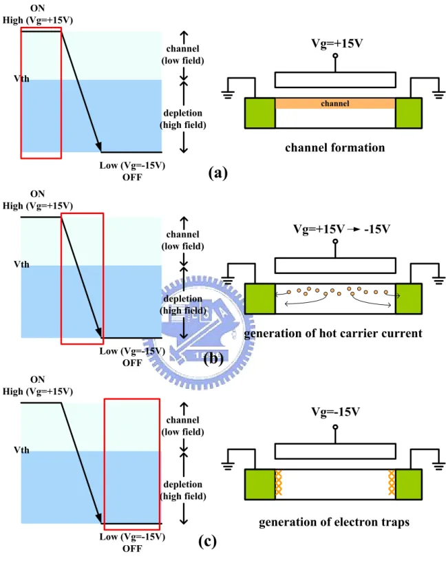
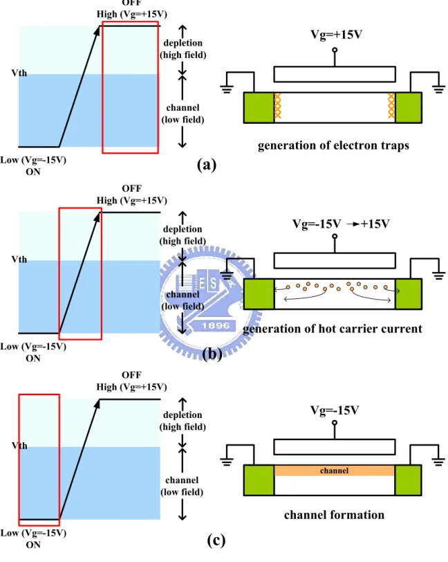
The degradation model under AC stress by Uraoka is described as follow. When the gate voltage is high (ON state and Vg=15V), the electrons gather to form a channel, as shown in Fig. 1-1 (a). When the gate voltage drops (ON→OFF and Vg=15V→-15V), the electrons in the channel move rapidly to the source and drain shown in Fig. 1-1 (b). Some of the trapped electrons are exposed to the high electric field and gain energy from the field. Hot electrons
are generated at this moment and form electron traps shown in Fig. 1-1 (c), result in the increase of density of state (DOS) in tail edge of poly-Si.
As for the P-type TFTs, when the gate voltage is low (ON state and Vg=-15V), the holes gather to form a channel shown in Fig. 1-2 (c). When the voltage transition from low to high (ON→OFF and Vg=-15V→15V), the holes in the channel move rapidly to the source and drain shown in Fig. 1-2 (b). Carriers gain energy from this electric field and become hot carriers. Therefore, more hot electrons are generated which causes trap formation at the grain boundaries around the drain edge shown in Fig. 1-2 (a).
ON High (Vg=+15V) Low (Vg=-15V) OFF channel (low field) depletion (high field) Vg=+15V channel formation channel Vth
(a)
ON High (Vg=+15V) Low (Vg=-15V) OFF channel (low field) depletion (high field) Vg=+15V -15Vgeneration of hot carrier current
Vth
(b)
ON High (Vg=+15V) Low (Vg=-15V) OFF channel (low field) depletion (high field) Vg=-15Vgeneration of electron traps
Vth
(c)
Vg=+15V
generation of electron traps
Vth
(a)
channel (low field) depletion (high field) Low (Vg=-15V) ON OFF High (Vg=+15V) Vg=-15V +15Vgeneration of hot carrier current
Vth
(b)
channel (low field) depletion (high field) OFF High (Vg=+15V) Low (Vg=-15V) ON Vg=-15V channel formation channel Vth(c)
channel (low field) depletion (high field) OFF High (Vg=+15V) Low (Vg=-15V) ON1.3 Motivation
In order to make LTPS TFTs suitable for advanced circuits, besides the improvement of performance of LTPS TFTs, the improvement of reliability is also significant. Therefore, reliability testing and understanding of reliability mechanisms become more and more necessary.
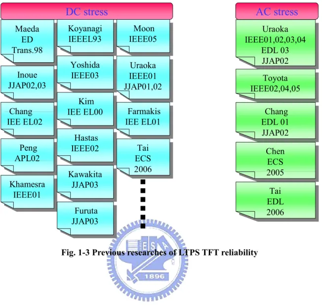
The reliability mechanisms of LTPS TFTs under DC (direct current) bias stress have been widely discussed . However, up to now, the reliability of LTPS TFTs under AC stress has been paid much less attention. The summary of previous researches are shown in Fig. 1-3. In the initial stage of practical applications, the LTPS TFTs used as switching elements for AMLCDs are operated in an AC mode, thus AC stress is much closer to real operational condition than conventional DC stress. In addition, unlike pixel TFTs, the TFTs in driver circuits are subjected to high-frequency voltage pulses. Finally, CMOS technology is necessary for driver circuits, which means that both the understanding of the reliability of N-type and P-type LTPS TFTs are important and necessary. Therefore, it is extremely important to understand the degradation mechanisms of N-channel and P-channel LTPS TFTs under AC stress.
In this study, the stressed mobility ratio to the initial value of N-channel and P-channel LTPS TFTs under various AC stress conditions. The stress conditions including swing range, and falling/rising times of the gate pulse, was discussed to verify the degradation mechanism under AC stress.
DC stress
Maeda ED Trans.98 Maeda ED Trans.98 Inoue JJAP02,03 Inoue JJAP02,03 Uraoka IEEE01 JJAP01,02 Uraoka IEEE01 JJAP01,02 Khamesra IEEE01 Khamesra IEEE01 Koyanagi IEEEL93 Koyanagi IEEEL93 Yoshida IEEE03 Yoshida IEEE03 Chang IEE EL02 Chang IEE EL02 Hastas IEEE02 Hastas IEEE02 Peng APL02 Peng APL02 Furuta JJAP03 Furuta JJAP03 Kim IEE EL00 Kim IEE EL00 Moon IEEE05 Moon IEEE05 Kawakita JJAP03 Kawakita JJAP03 Toyota IEEE02,04,05 Toyota IEEE02,04,05 Uraoka IEEE01,02,03,04 EDL 03 JJAP02 Uraoka IEEE01,02,03,04 EDL 03 JJAP02 Chang EDL 01 JJAP02 Chang EDL 01 JJAP02AC stress
Chen ECS 2005 Chen ECS 2005 Tai EDL 2006 Tai EDL 2006 Tai ECS 2006 Tai ECS 2006 Farmakis IEE EL01 Farmakis IEE EL01Chapter 2 Experimental Procedures
2.1 Procedures of Fabrication of LTPS TFTs
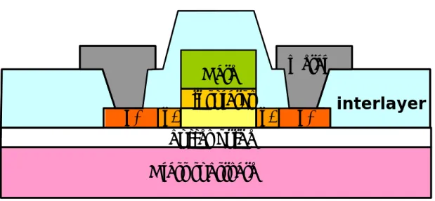
LTPS TFTs used in the experiment were the conventional top-gate structure and fabricated on glass substrates. The cross-section views of N-channel and P-channel LTPS TFTs are shown in Fig 2-1 and Fig. 2-2 respectively. The basic process flow is described as follows. Firstly, the buffer oxide and a-Si:H films were deposited on glass substrates by the PECVD system. Then, XeCl excimer laser was used to crystallize a-Si:H film followed with poly-Si active area definition. Subsequently, gate insulator was deposited by PECVD. The thickness of gate oxide is 650Å. Next, the metal gate formation and source/drain doping were performed. Dopant activation and hydrogenation was carried out after interlayer dielectric deposition. Finally, contact holes formation and metallization were performed to complete fabrication work. The lightly doped drain (LDD) structure was used in the N-channel TFTs to enhance hot carrier endurance while not used in P-type devices. The width/length of the TFT was 20μm/5μm. The TFTs of the same dimension will be used for reliability testing in the chapter 3 and chapter 4.
n+
n+
Glass substrate
buffer oxide
interlayer
metal
Gate
n-
insulator
Glass substrate
buffer oxide
Gate
p+
p+
metal
interlayer
insulator
Fig. 2-2 The cross-section views of P-channel LTPS TFTs
2.2 AC Stress Conditions
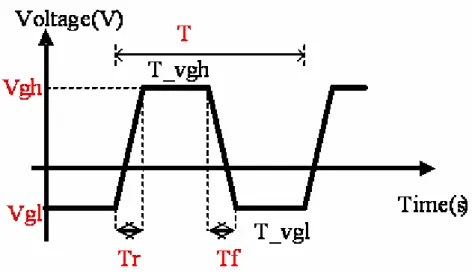
The Agilent 4156A semiconductor parameter analyzer with pulse generator was used to measure the I-V curve and stress the device with different conditions. The basic parameters of AC signal consists of frequency (F), signal high level (Vgh), signal low level (Vgl), high-level time (Vgh), low-level time (Vgl), rising time (Tr), and falling time (Tf). Fig. 2-3 shows the waveform of the AC signal. In AC signal, the definition of individual parameter is given as follow:
T = Tr + T_vgh + Tf + T_vgl (2.1) F = 1/T (2.2) Duty ratio = ( T_vgh+1/2 Tr+1/2 Tf )/T (2.3) where T is the signal period.
Fig. 2-3 Waveform and definition of the AC signal
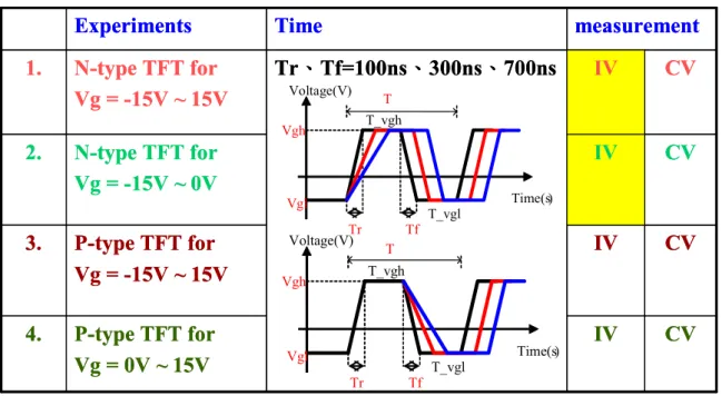
Under AC stress, pulse voltage was applied to the gate electrode and source and drain were grounded, which is shown in Fig. 2-4. The standard stress condition in the experiment is the gate voltage swing of -15 V to 15 V, F = 500 kHz, Tr and Tf are both 100ns, and duty ratio is 50%. These parameters can be adjusted and then various stress conditions on the gate electrode are performed to examine the reliability of LTPS TFTs. To investigate which parameter of the stress parameters dominates the degradation of the N-channel and P-channel TFTs transfer characteristics, Tr and Tf from 100ns to 700ns are changed for gate swing range of -15 V to 15 V. Secondly, the effects at Tr and Tf for the gate swing in the depletion region are studied. The experimental conditions is shown in table 2-1.
TFT
Stress
Stress
G
D
S
Glass substrate buffer oxide Gate p+ p+ metal interlayer insulatorTable 2-1 The experiment condition forms of the N-type and P-type. IV IV IV IV measurement Tr、Tf=100ns、300ns、700ns Time P-type TFT for Vg = 0V ~ 15V N-type TFT for Vg = -15V ~ 0V N-type TFT for Vg = -15V ~ 15V Experiments CV 4. CV 2. CV 1. P-type TFT for Vg = -15V ~ 15V CV 3. IV IV IV IV measurement Tr、Tf=100ns、300ns、700ns Time P-type TFT for Vg = 0V ~ 15V N-type TFT for Vg = -15V ~ 0V N-type TFT for Vg = -15V ~ 15V Experiments CV 4. CV 2. CV 1. P-type TFT for Vg = -15V ~ 15V CV 3.
Number of Repetition is the same.
T_vgh T_vgl Time(s) Voltage(V Vgh Vgl Tr Tf ) T T_vgh T_vgl Time(s) Voltage(V) Vgh Vgl Tr Tf T
In order to compare the different stress conditions and attain the faithful stressed behavior, a large amount of devices should be stressed and compared. However, the existence of grain boundaries in the channel might make the degradation behavior more complicated, and it may be therefore be more difficult to find the dominant parameters of AC stress. In prior study [22], the diverse degradation behaviors occur due to different sources of LTPS TFTs and variation of the initial value of extracted parameter. In this work, crosstie devices were adopted for the consistency of the initial device behaviors.
2.3 Parameter Extraction Method
For most of the researches on TFT, the constant current method is widely-used to determine the threshold voltage (Vth). The threshold voltage in the thesis is determined from
this method, which extracts Vth from the gate voltage at the normalized drain current
N D eff eff
The transfer characteristics of poly-Si TFTs are similar to those of conventional MOSFETs. The MOSFETs can be applied to the poly-Si TFTs, so the first order I-V relation in the bulk Si. The field effect mobility (Mu, µFE) is derived from the maximum value of the
transconductance gm, which can be expressed as:
2 1 [( ) ] 2 D FE ox G th D D W I C V V V V L μ = − − (2-4) Where
Cox is the gate capacitance per unit area, W is channel width,
L is channel length,
Vth is the threshold voltage.
If the drain voltage VD is much smaller as compared with(VG −Vth) (i.e. VD << VG - Vth),
then the drain current can be approximated as:
D TH G ox FE D V V V L W C I =μ ( − ) (2-5)
And the transconductance is defined as:
D FE ox const V G D m V L WC V I g D
μ
= ∂ ∂ = = .Therefore, the field effect mobility can be expressed as:
m
g
F E ox DL
C W V
μ=
(2-6)In other words, the field-effect mobility can be extracted by taking the maximum value of the gm into (2-6) when VD = 0.1V
2.4 C-V Measurements
The C-V curves of the gate-to-drain capacitance (CGD) before and after stress at different
Since it is difficult to observe the defect position in TFTs with the I-V characteristic, the C-V measurement is used to examine the information about position and type of degradation in the device after stress [23]. For instance, if carriers are trapped by defects, C-V curve stretch out slightly, or if states are generated additionally, C-V curve increase somewhat in the depletion region. Besides, the C-V curves are helpful to identify whether the dominant mechanism of degradation is the increase of fixed charges or trap states. In this work, since the degradation should be symmetric for the gate-to-source and gate-to-drain case, the C-V curves are obtained only for the Cgd curves measured between the drain and the gate.
Chapter 3 N-type Poly-Si TFT under Gate
Pulse Stress
3.1 Behavior of I-V curve after stressing
3.1.1 Rising Time and Falling Time for Vg of ON and
OFF Region
The transient time dependence for the degradation was examined as shown in Fig. 3-1. During the variation of rising time Tr from 100 ns to 700 ns with a fixed Tf of 100 ns, no significant change in μ/μ0 was observed as shown in Fig. 3-1 (a). On the contrary, the
degradation depended strongly on the falling time Tf as shown in Fig. 3-1 (b). The degradation is remarkably accelerated with the decrease of the falling time from 700 ns for 100 ns for a fixed Tr of 100 ns. In the case of changing rising time, the gate voltage varies from OFF region to ON region, and the mobile carriers are sited at so low electrical field that no device degradation is formed. But in the case of changing falling time, the gate voltage varies from ON region to OFF region, some carries remain in the channel and are sited at high electrical field to be hot carries.
universal curve
1E7 1E8 1E9
0.0 0.1 0.2 0.3 0.4 0.5 0.6 0.7 0.8 0.9 1.0 u/u 0 Number of Repetition tr100tf100 tr300tf100 tr700tf100 Tr Tr '
Fig. 3-1 (a) Degradation of μ/μ0 in N-channel TFT under AC stress with Vg = -15 V to 15
V measured for various rising times Tr and for Tf = 100 ns.
1E7 1E8 1E9
0.0 0.1 0.2 0.3 0.4 0.5 0.6 0.7 0.8 0.9 1.0 u/ u 0 Number of Repetition tr100tf100 tr100tf300 tr100tf700 Tf Tf '
Fig. 3-1 (b) Degradation of μ/μ0 in N-channel TFT under AC stress with Vg = -15 V to 15
3.1.2 Rising Time and Falling Time for Vg in the OFF
Region
In prior study, we have known that degradation by pulse swing for the ON region was very small, however, that by pulse swing for the OFF region was large. We have already observed the transient time dependence for the degradations of N-channel TFTs under AC stress with Vg = -15 V to 15V. For the gate swing of -15 V to 15 V, it consists of Vg = -15 V to 0V and Vg =0 V to 15V. For N-channel TFT, Vg = -15 V to 0V is OFF region, and Vg =0 V to 15V is ON region. Because no device degradation is formed for N-channel TFT under AC stress with Vg = 0 V to 15 V, we are only interested in the transient time dependence for the degradation of N-channel TFT at Vg = -15 V to 0V. For the gate voltage swings from -15 V to 0 V, it is firstly observed that the degradation is obviously dependent on both the rising time and falling time, as shown in Fig. 3-2 (a) and Fig. 3-2 (b). Since there are no induced electrons for these applied gate voltages, it reveals that the previously proposed model may be incomplete.
1E7 1E8 1E9 0.0 0.1 0.2 0.3 0.4 0.5 0.6 0.7 0.8 0.9 1.0 u/ u 0 Number of Repetition tr100tf100 tr300tf100 tr700tf100 Tr Tr '
Fig. 3-2 (a) Rising time dependence of the degradation.
1E7 1E8 1E9
0.0 0.1 0.2 0.3 0.4 0.5 0.6 0.7 0.8 0.9 1.0 u/u 0 Number of Repetition tr100tf100 tr100tf300 tr100tf700 Tf Tf '
3.2 Behavior of C-V curve after stressing
It is entirely fair to say that I-V measurements could reveal the whole channel’s characteristics which would not afford to provide detailed information about the mechanism of devices. Therefore, C-V measurement would become essential for delicate analysis [24-26]. Generally speaking, the C-V measurement is characterized by its ability of revealing characteristics of gate-to-source and gate-to-drain instead of the whole channel.
In this section, the gate-to-drain capacitance CGD of N-type and P-type devices are
measured with frequencies of 1MHz. The CGD curve is measured with a floating source.
Besides, the curves are plotted with normalized value of capacitances, which means the ratio of the measured value to the maximum value of the capacitance.
3.2.1 Rising Time and Falling Time for Vg of ON and
OFF Region
The transient time dependence for the degradation was examined as shown in Fig. 3-3. During the variation of rising time Tr from 100 ns to 700 ns with a fixed Tf of 100 ns, no significant change in C/Cox was observed as shown in Fig. 3-3 (a). On the contrary, the degradation depended strongly on the falling time Tf as shown in Fig. 3-3 (b). The degradation is remarkably accelerated with the decrease of the falling time from 700 ns for 100 ns for a fixed Tr of 100 ns.
universal curve
-10 -5 0 5 10 0.0 0.2 0.4 0.6 0.8 1.0 C/Cox Gate Voltage (V) tr100tf100 tr300tf100 tr700tf100Fig. 3-3 (a) Degradation of C/Cox in N-channel TFT after AC stress with Vg = -15 V to 15 V with various rising times Tr and for Tf = 100 ns measured at 1MHz.
-10 -5 0 5 10 0.0 0.2 0.4 0.6 0.8 1.0 C/Cox Gate Voltage (V) tr100tf100 tr100tf300 tr100tf700
Fig. 3-3 (b) Degradation of C/Cox in N-channel TFT after AC stress with Vg = -15 V to 15 V with various rising times Tf and for Tr = 100 ns measured at 1MHz.
3.2.2 Rising Time and Falling Time for Vg in the OFF
Region
The transient time dependence for the degradation was examined as shown in Fig. 3-4. The degradation is obviously dependent on both the rising time and falling time, as shown in Fig. 3-4 (a) and Fig. 3-4 (b).
-10 -5 0 5 10 0.0 0.2 0.4 0.6 0.8 1.0 C/Co x Gate Voltage (V) tr100tf100 tr300tf100 tr700tf100
Fig. 3-4 (a) Degradation of C/Cox in N-channel TFT after AC stress with Vg = -15 V to 0 V with various rising times Tr and for Tf = 100 ns measured at 1MHz.
-10 -5 0 5 10 0.0 0.2 0.4 0.6 0.8 1.0 C/Cox Gate Voltage (V) tr100tf100 tr100tf300 tr100tf700
Fig. 3-4 (b) Degradation of C/Cox in N-channel TFT after AC stress with Vg = -15 V to 0 V with various rising times Tf and for Tr = 100 ns measured at 1MHz.
3.3 Experimental Results and Discussion
3.3.1 Simulation result of Using TFT’s Slicing Model
3.3.1.1 Factors of Degradation Mechanism
In order to analyze the degraded phenomena, two factors are taken into consideration, that is, the transient electric field in the lateral direction and the changes in the number the channel electrons under the lateral voltage difference. To understand the transient fields and charge distributions in the channel, a slicing method is used on the device for simulation. A whole TFT is sliced into many shorter ones in series, and a short TFT consists of segment of channel resistance and gate oxide, as shown in inset of Fig. 3-5.
Fig. 3-5 TFT’s slicing model
3.3.1.2 The Transient Voltage Distribution in the TFT
Channel
For simplicity, ten short TFTs are used in the slicing model. Because source and drain are grounded, the channel voltage is symmetric in the middle of the channel. The voltage of the edge TFT is called Ve, and the other voltages are V21, V32, V43, V54, respectively, as shown in
Fig 3-6 (a).
Using a commercially available circuit simulator SPECTRE, the transient voltage distribution in the TFT channel under AC stress can be qualitatively expressed. Firstly, we observe the transient voltage distribution in the channel of TFT under AC stress with Vg = -15 V to 15 V, Ve is the largest voltage among the sliced node voltages, shown in Fig. 3-6 (b). Referring to the previous report, the emission image of the N-channel TFT under dynamic stress indicates that the degradation is the worst at the edges of the channel, shown in Fig.
3-6(c). It also accords with the simulation results that Ve is the largest voltage in the channel. In this section, we call ON region as channel region, and OFF region as depletion region. In the channel region, the channel voltages are almost zero. On the contrary, in the depletion region, the channel voltages are very large. Therefore, device degradation mainly occurs in the depletion region, and not in the channel region.
Fig. 3-6 (a) 10 TFT’s slicing model
Dynamic Stress
Vg=+/-15V
f=500KHz
Photon Emission
Photon Emission
Dynamic Stress
Vg=+/-15V
f=500KHz
Photon Emission
Photon Emission
Fig. 3-6 (c) Photon emission
3.3.1.3 An indexΠto estimate the degraded degree
In order to describe the degree of the degradation, the index Π calculated from simulation result is further introduced, which is given as
∫
∑
• • − • = Π Ti dt dt Ve Vg d Cox Ve Ti [ ( )/ ] 1 (2-7)where Ti corresponds to Tr, Tf, T_vgh, and T_vgl, and Cox is the gate capacitance per unit area. This index accounts for two factors. The first one is Ve, corresponding to the transient lateral electrical field at the edge of the sliced TFT. And the second term is Coxy d(Vg – Ve) / dt, representing the charges flow outward through the edge of the sliced TFT. For simplicity,
we assume that Ve follows the change of Vg at Tr and Tf, thus Vg – Ve is kept constant and its time differentiation is zero. Therefore, the coupling magnitude of Ve and its duration dominate the value of Π. The mobility degradation (1-μ/μ0) versus the index Π under different AC
stress conditions are plotted in Fig. 3-7. The fair linearity exhibits the validity of the proposed mechanism.
Fig. 3-7 Mobility degradation (1-μ/μ0) versus Index Π for N-channel TFT
3.3.2 Slight Stretch out phenomenon of C-V curve
In prior study, we have known that the mechanism of degradtion under AC stress for the LTPS TFTs is similar hot carrier. Hot carrier which will be introduced in detail as follows.
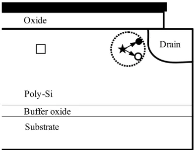
Hot-carrier effects are the sources of serious device degradation because of the charging of the gate oxide in the N-channel TFT. The basic mechanism of hot-carrier aging is shown in Fig. 3-8. Channel electrons gain energy in the high-field region of the drain and are accelerated towards the gate oxide. This causes the charge to be injected into the gate oxide and creates a fixed charge in the oxide.
Charge damage occurs at these voltages through a three-step mechanism that causes an energy enhancement resulting from a feedback mechanism, namely impact-ionization feedback through the drain-bulk junction.
Oxide
Drain
Substrate Buffer oxide Poly-Si
Fig. 3-8 Hot-electron generation at the drain of the MOSFET, resulting from impact ionization at high fields. [27.]
DC hot carrier stressing condition which the gate to source voltage VGS = 2V ~ threshold
voltage and the drain to source voltage VGD is 20V. Previous study’s hypothesis can explain
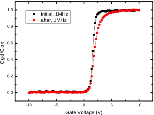
the I-V curve’s degradation after hot carrier stress but they don’t examine their suggestion by C-V measurement or simulation. As shown in Fig. 3-9, the normalized CGD curves have a
slight stretch out after stressing 500sec with measurement frequency of 1MHz. This phenomenon indicates that only degradation around the drain region does occur. The simulated Capacitance-Voltage curve has stretch out slightly as shown in Fig. 3-10. The simulation result and model structure shown in Fig. 3-11 is quite consistent with our experiment result and have a fair response to the previous study. In crystal silicon, hot carriers increase the interface states density or generate traps in the oxide. However, in the case of poly-Si TFT, hot carriers increase the DOS of poly-Si near drain, causing the decrease of mobility.
-10 -5 0 5 10 0.0 0.2 0.4 0.6 0.8 1.0 C gd/ C o x Gate Voltage (V) initial, 1MHz after, 1MHz
Fig. 3-9 Normalized CGD curve stretchs out before and after hot carrier stress 500sec at
measurement frequency 1MHz -10 -5 0 5 10 -0.2 0.0 0.2 0.4 0.6 0.8 1.0 -10 -5 0 5 10 -0.2 0.0 0.2 0.4 0.6 0.8 1.0
Curve B, with states in thin film near drain
Gate Voltage (V) Normali z ed ca pacit a nce Curve A, without trap states
Fig. 3-11 The model of the cross section of the device after hot carrier stress
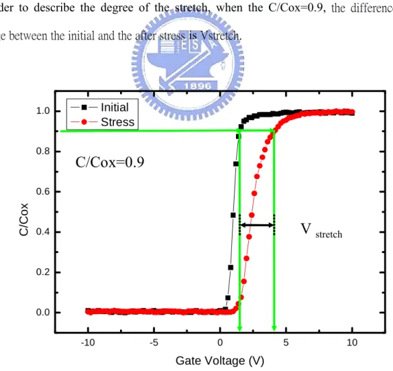
As shown in Fig. 3-12, the normalized CGD curves have a slight stretch out after stressing.
In order to describe the degree of the stretch, when the C/Cox=0.9, the difference of gate voltage between the initial and the after stress is Vstretch.
-10 -5 0 5 10 0.0 0.2 0.4 0.6 0.8 1.0 C/ Co x Gate Voltage (V) Initial Stress
C/Cox=0.9
V
stretchThe mobility decrease ratio versus the voltage stretch of C-V measurement under different AC stress conditions are plotted in Fig.3-13. For the gate voltage swings from -15 V to 15 V, the variation of mobility decrease ratio, no significant change in both mobility decrease ratio and the voltage stretch as shown by the circled in Fig. 3-13 (a). On the contrary, their degradation are positively correlated for the data of changing the falling time Tf.
For the gate voltage swings from -15V to 0V, the variation of mobility decrease ratio and voltage stretch are both influenced by Tr and Tf, as shown in Fig. 3-13 (b).
0.0 0.5 1.0 1.5 2.0 2.5 3.0 3.5 0.0 0.2 0.4 0.6 0.8 1.0 u/u0
Voltage stretch out (V)
tr100tfx trxtf100
Fig. 3-13 (a) mobility decrease ratio versus voltage shift of C-V measurement for pulse stress of Vg=-15V~15V.
0.0 0.5 1.0 1.5 2.0 2.5 0.0 0.2 0.4 0.6 0.8 1.0 u/u0
Voltage of stretch out (V)
tr100tfx trxtf100
Fig. 3-13 (b) mobility decrease ratio versus voltage shift of C-V measurement for pulse stress of Vg= -15V~0V.
3.4 Summary
Table 3-1 Summary statement of experimental result for N-type.
Vg = -15V~0V
Curve stretch Tr
Tf
Behavior of C-V curve
for Vg in the depletion
Region
4
Vg=-15V~15V
Curve stretch Tr
Tf
Behavior of C-V curve
for Vg ON/OFF
3
Vg = -15V~0V
Mobility decrease Tr
Tf
Gate voltage leveling
for Vg in the depletion
Region
2
Vg=-15V~15V:
Mobility decrease Tr
Tf
Gate voltage leveling
for Vg ON/OFF
1
Phenomena
Experiments
Vg = -15V~0V
Curve stretch Tr
Tf
Behavior of C-V curve
for Vg in the depletion
Region
4
Vg=-15V~15V
Curve stretch Tr
Tf
Behavior of C-V curve
for Vg ON/OFF
3
Vg = -15V~0V
Mobility decrease Tr
Tf
Gate voltage leveling
for Vg in the depletion
Region
2
Vg=-15V~15V:
Mobility decrease Tr
Tf
Gate voltage leveling
for Vg ON/OFF
1
Phenomena
Experiments
For AC stress with the gate voltage toggling between -15 V and 15 V, it is observed that the degradation depends on the falling time Tf of the gate pulse but does not depend on the rise time Tr. However, for the gate voltage swinging from -15 V to 0 V, it is observed that the degradation is both influenced by Tr and Tf.
The I-V measurement of N-type is mobility decrease. The C-V curve degradation phenomenon is slight stretch out, which is positively correlatced to the confirmed to be the I-V degradation. The mechanism of degradation under AC strss for N-type poly-Si TFT is hot carrier effect according to both I-V and C-V measurements.
A slicing method is used for the simulation of channel voltage distribution and the change in the number of the carriers at the edge to explain the degradation behaviors. The index Π considering the two factors is introduced and it shows good linearity with the mobility degradation for various gate pulse stress conditions.
Chapter 4 P-type Poly-Si TFT under Gate
Pulse Stress
4.1 Behavior of I-V curve after stressing
4.1.1 Rising Time and Falling Time for Vg of ON and
OFF Region
The transient time dependence for the degradation of P-channel TFT was also studied. The dependence of the mobility change on rising time and falling time is shown in Fig. 4-1(a) and 4-1(b), respectively. For P-channel TFT, the change was accelerated for a variation in rising time, however, the change was not affected by the falling time. In the case of changing rising time, the gate voltage varies from ON region to OFF region, and some carriers are sited at so high electrical field that device degradation is formed. But in the case of changing falling time, the gate voltage varies from OFF region to ON region, carriers are sited at low electrical field not becoming hot carries.
1E7 1E8 1E9 1.12 1.14 1.16 1.18 1.20 1.22 u/ u0 Number of Repetition tr100tf100 tr300tf100 tr700tf100 Tr Tr '
Fig. 4-1 (a) Degradation of μ/μ0 in P-channel TFT stressed by gate pulses with various
rising times Tr and keeping Tf at 100 ns.
1E7 1E8 1E9
1.12 1.14 1.16 1.18 1.20 1.22 u/ u 0 Number of Repetition tr100tf100 tr100tf300 tr100tf700 Tf Tf '
universal curve
Fig. 4-1 (b) Degradation of μ/μ0 in P-channel TFT measured for various falling times Tf
4.1.2 Rising Time and Falling Time for Vg in the OFF
Region
For P-channel TFT, Vg = 0V to 15V is OFF region, and Vg =-15V to 0V is ON region. Because no device degradation is formed for P-channel TFT under AC stress with Vg =-15V to 0V, we are also only interested in the transient time dependence for the degradation of P-channel TFT at Vg = 0V to 15V. For the gate voltage swings from 0V to 15V, it is observed that the degradation is dependent on the rising time but independent of falling time, which is the same as P-channel TFT under AC stress with Vg =-15 V to 15 V, as shown in Fig. 4-2 (a) and Fig. 4-2 (b).
1E7 1E8 1E9
1.04 1.06 1.08 1.10 1.12 1.14 1.16 1.18 1.20 1.22 u/ u0 Number of Repetition tr100tf100 tr300tf100 tr700tf100 Tr Tr '
Fig. 4-2 (a) Degradation of μ/μ0 in P-channel TFT under AC stress with Vg = 0 V to 15 V
1E7 1E8 1E9 1.12 1.14 1.16 1.18 1.20 1.22 u/ u0 Number of Repetition tr100tf100 tr100tf300 tr100tf700 Tf Tf '
universal curve
Fig. 4-2 (b) Degradation of μ/μ0 in P-channel TFT under AC stress with Vg = 0 V to 15 V
measured for various rising times Tf and for Tr = 100 ns.
4.2 Behavior of C-V curve after stressing
4.2.1 Rising Time and Falling Time for Vg of ON and
OFF Region
The transient time dependence for the degradation was examined as shown in Fig. 4-3. During the variation of rising time Tr from 100 ns to 700 ns with a fixed Tf of 100 ns, the degradation depended strongly on the rising time Tr as shown in Fig. 4-3 (a). On the contrary, no significant change in C/Cox was observed as shown in Fig. 4-3 (b). The degradation is remarkably accelerated with the decrease of the rising time from 700 ns for 100 ns for a fixed Tf of 100 ns.
-10 -5 0 5 10 0.0 0.2 0.4 0.6 0.8 1.0 C/Cox Gate Voltage (V) tr100tf100 tr300tf100 tr700tf100
Fig. 4-3 (a) Degradation of C/Cox in P-channel TFT under AC stress with Vg = -15 V to 15 V measured for various rising times Tr and for Tf = 100 ns.
universal curve
-10 -5 0 5 10 0.0 0.2 0.4 0.6 0.8 1.0 C/Cox Gate Voltage (V) tr100tf100 tr100tf300 tr100tf700Fig. 4-3 (b) Degradation of C/Cox in P-channel TFT under AC stress with Vg = -15 V to 15 V measured for various rising times Tf and for Tr = 100 ns.
4.2.2 Rising Time and Falling Time for Vg in the OFF
Region
The transient time dependence for the degradation was examined as shown in Fig. 4-4. During the variation of rising time Tr from 100 ns to 700 ns with a fixed Tf of 100 ns, the degradation depended strongly on the rising time Tr as shown in Fig. 4-4 (a). On the contrary, no significant change in C/Cox was observed as shown in Fig. 4-4 (b). The degradation is remarkably accelerated with the decrease of the rising time from 700 ns for 100 ns for a fixed Tf of 100 ns. -10 -5 0 5 10 0.0 0.2 0.4 0.6 0.8 1.0 C/ Cox Gate Voltage (V) tr100tf100 tr300tf100 tr700tf100
Fig. 4-4 (a) Degradation of C/Cox in P-channel TFT under AC stress with Vg = 0 V to 15
universal curve
-10 -5 0 5 10 0.0 0.2 0.4 0.6 0.8 1.0 C/Cox Gate Voltatge (V) tr100tf100 tr100tf300 tr100tf700Fig. 4-4 (b) Degradation of C/Cox in P-channel TFT under AC stress with Vg = 0 V to 15 V measured for various rising times Tf and for Tr = 100 ns.
4.3 Experimental Results and Discussion
4.3.1 Simulation Result Using TFT’s Slicing Model
Using a commercially available circuit simulator SPECTRE, the transient voltage distribution in the TFT channel under AC stress can be qualitatively expressed. Firstly, we observe the transient voltage distribution in the channel of TFT under AC stress with Vg = -15 V to 15 V, Ve is the largest voltage among the sliced node voltages, shown in Fig. 4-5. It also accords with the simulation results that Ve is the largest voltage in the channel. In the channel region, the channel voltages are almost zero. On the contrary, in the depletion region, the channel voltages are very large. Therefore, device degradation mainly occurs in the depletion region, and not in the channel region.
Fig. 4-5 The transient voltage distribution of P-channel TFT.
For the simulation with the transient time of P-channel TFT under AC stress at Vg = -15 V to 15 V, Ve is shown in Fig. 4-6. Like the simulation result of N-channel TFT, when Vg rises in the depletion region, Ve follows the change of Vg owing to coupling effect, and then Ve slightly discharging shows some mobile charges will be speed up in the high electrical filed to become hot carriers. The coupling magnitude of this transient electrical field becomes larger with shorter Tr, resulting in the Tr dependence of the mobility degradation. As the gate voltage falls to the channel region, Ve is quickly discharged to zero, such that the lateral field is too low to speed up the carriers. Therefore, the mobility degradation is independent of Tf.
Next, we observe Ve for the gate voltage swing of 0V to 15V, shown in Fig. 4-7. Since the gate voltage is all below VTH, TFT is kept in the depletion region. But from the simulation
result, Ve goes high at Tr to T_vgh, but goes low at Tf to T_vgl. So the degradation is only dependent on Tr, not dependent on Tf. The simulation result accords with the measurement data.
Fig. 4-6 (a) Ve for Vg = -15 V ~15 V of Tr = Tf = 100 ns
Fig. 4-6 (c) Ve for Vg = -15 V ~ 15V of Tr = 100 ns, Tf = 700 ns
Fig. 4-7 (b) Ve for Vg = 0 V ~ 15 V of Tr = 700 ns, Tf = 100 ns
Fig. 4-7 (c) Ve for Vg = 0 V ~ 15V of Tr = 100 ns, Tf = 700 ns
The mobility degradation (μ/μ0-1) versus the index Π under different AC stress conditions
Fig. 4-8 Mobility degradation (μ/μ0-1) versus Index Π for P-channel TFT
4.3.2 C-V increase in the depletion region
4.3.2.1 DC hot carrier stress
Previous study of P-type TFT’s degradation behavior under hot carrier stress is that the increase of mobility, the increase of on current and no obvious degradation on subthreshold swing [28]. The DC hot carrier stressing condition of is the gate voltage VG=-2V and the drain
voltage VD=-20V is conducted on our P-type TFT and the same degradation behavior as
aforementioned is observed and shown in Fig 4-9.The degradation mechanism of P-type TFT is commonly considered as: the increase of on current and the increase of transconductance without any variation of subthreshold slope and threshold voltage maybe attributed to facts that the interface characteristics of the channel was not affected and the effective channel length was reduced during hot carrier stress. It has been reported that these phenomenon are caused with the electron trapping into gate insulator near the drain. When the electrons are
trapping into gate insulator near the drain, the holes are accumulated in the channel edge near the drain due to local electrical field so that the effective drain region is extended to the active channel.
The C-V measurements are further employed to investigate the degradation mechanism. As shown in Fig 4-10, gate-to-drain capacitance CGD curves after stress with different
frequencies have the extra increase for the positive gate voltage. The CGD curve increases
slightly when the gate voltage is smaller than the Vth. The extra increase for the lower gate voltage of CGD curve may be attributed to the interface trapped charges, which may be caused
by the high voltage difference between the gate and the drain during the stress. The C–V measurement results further support the creation of the trap charges on the surface near drain. The increase of CGD for the gate voltage below Vth indicates the increase of carriers which is
induced by the trapped electrons near drain.
The model of the cross section of the device after DC stress is shown in Fig. 4-11. As shown in Fig. 4-12, the simulation results with and without degraded regions in the device. Curve A is the C-V curve with no degraded region, while curve B is the one with interface charges near the drain region. Comparing to curve A, curve B increases slightly for the gate voltage below Vth. It reveals that the interface charges between the drain and the gate influence the number of induced carriers in channel depletion and weak inversion conditions. According this prior study, we have known that capacitance increases slightly and mobility increases might be dependent on the same degradation mechanism.
-10 -8 -6 -4 -2 0 2 4 10-13 10-12 10-11 10-10 10-9 10-8 10-7 10-6 -10 -8 -6 -4 -2 0 2 4 0.0 2.0x10⁻⁷ 4.0x10⁻⁷ 6.0x10⁻⁷ 8.0x10⁻⁷ 1.0x10⁻⁶ 1.2x10⁻⁶ Dra in Curre nt (A) IV_after stress IV_before stress Gm_after stress Gm_bsfore stress Tra n s c onduc ta nce (S) Gate Voltage (V)
Fig. 4-9 The degradation of I-V transfer characteristic of P-type TFT after hot carrier stressing (VGS = -2V~threshold voltage and VGD= -20V) 1000sec
-5 0 5 0.0 0.2 0.4 0.6 0.8 1.0
Normalized Capacitance C
GDGate Voltage (V)
initial,1MHz initial,50KHz after,1MHz after,50KHzFig. 4-10 The gate-to-drain capacitance CGD curves of P-type crosstie TFT before and
Fig. 4-11 The model of the cross section of the device after stress (VG = -2V and VD = -20V) 1000sec. -10 -5 0 5 10 -0.2 0.0 0.2 0.4 0.6 0.8 1.0 -10 -5 0 5 10 -0.2 0.0 0.2 0.4 0.6 0.8 1.0
Normali
z
ed Capaci
tance
Gate Voltage (V) Curve A, with no trap charges Curve B, with trap chargesFig. 4-12 The simulation result of C-V curve before and after stress
4.3.2.2 AC stress
As shown in Fig. 4-13, the normalized CGD curves have a Cmin increase after stressing. In
order to describe the degree of the Cmin increase, when the Vg=-0.8, the difference of normalized CGD between the initial and the after stress is ΔC.
-10 -5 0 5 10 0.0 0.2 0.4 0.6 0.8 1.0 C/C o x Gate Voltage (V) Initial Stress
Vg=-0.8V
ΔC
Fig. 4-13 The ΔC of C-V curve before and after stress
The mobility increases ratio versus the capacitance increases ratio was examined as shown in Fig.4-14. During the variation of rising time Tr from 100 ns to 700 ns with a fixed Tf of 100 ns, the mobility increases ratio depended strongly on the capacitance increases ratio. On the contrary, no significant change in falling time from 100ns to 700ns with a fixed Tr of 100ns.
0.04 0.05 0.06 0.07 0.08 0.09 0.10 1.06 1.08 1.10 1.12 1.14 1.16 1.18 1.20 1.22 u/u 0 C% tr100tfx trxtf100 ΔC
Fig. 4-14 (a) Degradation ratio (u%) versus the capacitance increases ratio of Vg=-15V~15V 0.04 0.05 0.06 0.07 0.08 0.09 0.10 1.06 1.08 1.10 1.12 1.14 1.16 1.18 1.20 1.22 u/u0 C% tr100tfx trxtf100 ΔC
Fig. 4-14 (b) Degradation ratio (u%) versus the capacitance increases ratio of Vg=0V~15V
The degradation of P-channel TFT devices is due to a different mechanism rather than that of the N-channel TFT devices. The mechanism is triggered by the electrons in the inversion region of the channel that are injected into the gate oxide. The trapped electrons cause the surface of the channel to invert, which effectively extends the p+ region of the drain into the channel. Fig. 4-15 shows this mechanism and indicates the charged area effectively extending the drain. Extending the drain reduces the effective channel length of the transistor and actually increases the transconductance as a function of the time the device is operated at a high voltage. The mechanism is called hot-electron-induced punchthrough (HEIP). This is the dominant cause of P-channel TFT device degradation.
Gate P+ P+ Drain Source -+ -Leff P -Vd<0V Vg<0V Gate P+ P+ Drain Source -+ + + Leff P -Inversion Layer Vd<0V Vg<0V
|Vg|<|Vd|
Fig. 4-15 Schematic illustration of the mechanism causing the HEIP effect
We consider the relationship between ΔL and capacitance increase slightly.
(
C)
A
C
W
d
d
L
ε
ε
Δ
Δ = ×
= ×
Δ
,where C is the increase slightly of CGD for the gate voltage below Vth.
In prior study, we have known that the CGD curve is measured with a floating source.
CMH:-10~10V
channelCML
ΔL 1 2 ΔL 1 2floating
Fig. 4-16 The relationship betweenΔL and ΔLc in C-V measurement.
We futher deduct the relationship between ΔL and mobility increase.
( ) L L Lμ
μ
μ
μ
+ Δ = − Δ ,where Δμ is the mobility increase after a stress. The ΔLμ is identical to ΔL as shown in Fig .4-17.
Vg=-10~10V
channelVd=0.1V
ΔL 1 2 ΔL 1 2Fig. 4-17 The relationship betweenΔLμ and ΔL in C-V measurement.
And then, we observe the relation of mobility increase and capacitance increase with ΔL. The ΔLμ versus ΔLc under different AC stress conditions are plotted in Fig. 4-18 (a) and Fig.4-18 (b). It can be seen that the relationship of the ΔLμ and ΔLc is almost linear with a
slope of 2. In addition, we find that ΔLμ are two times of the ΔLc. So, our assumption is established. 0.00 0.05 0.10 0.15 0.20 0.25 0.30 0.35 0.40 0.0 0.1 0.2 0.3 0.4 0.5 0.6 0.7 0.8 0.9
VgX1515
Linear fit
Lu Lcy=2.1918x
R
2=0.9886
ΔLC Δ Lμ0.00 0.05 0.10 0.15 0.20 0.25 0.30 0.35 0.40 0.45 0.50 0.0 0.1 0.2 0.3 0.4 0.5 0.6 0.7 0.8 0.9 Lu LC
Vg015V
Linear fit
y=1.9387x
R2=0.8118
ΔLC Δ LμFig. 4-18 (b) ΔLμ versus ΔLc for pulse stress of Vg=0V~15V.
4.4 Summary
Table 4-1 Summary statement of experimental result for N-type.
Vg = 0V~15V
Curve of increases slightly Tr
Tf
Behavior of C-V curve
for Vg in the depletion
Region
4
Vg=-15V~15V
Curve of increases slightly Tr
Tf
Behavior of C-V curve
for Vg ON/OFF
3
Vg = 0V~15V
Mobility increase Tr
Tf
Gate voltage leveling
for Vg in the depletion
Region
2
Vg=-15V~15V:
Mobility increase Tr
Tf
Gate voltage leveling
for Vg ON/OFF
1
Phenomena
Experiments
Vg = 0V~15V
Curve of increases slightly Tr
Tf
Behavior of C-V curve
for Vg in the depletion
Region
4
Vg=-15V~15V
Curve of increases slightly Tr
Tf
Behavior of C-V curve
for Vg ON/OFF
3
Vg = 0V~15V
Mobility increase Tr
Tf
Gate voltage leveling
for Vg in the depletion
Region
2
Vg=-15V~15V:
Mobility increase Tr
Tf
Gate voltage leveling
for Vg ON/OFF
1
Phenomena
Experiments
For AC stress with the gate voltage toggling between -15 V and 15 V, it is observed that the degradation depends on the rising time Tr of the gate pulse but does not depend on the falling time Tf, which is similar to the result for the pulse stress with the gate voltage toggling between 0 V and 15 V.
The I-V measurement of P-type is mobility increase. The C-V curve degradation phenomenon is capacitance increase in the depletion region, which is positively correlateced to the confirmed to be the I-V degradation. The mechanism of degradtion under AC strss for P-type poly-Si TFT is channel length shortening effect according to both I-V and C-V measurements. Beside △L is almost to the degradation degree.
A slicing method is used for the simulation of channel voltage distribution and the change in the number of the carriers at the edge to explain the degradation behaviors. The index Π considering the two factors is introduced and it shows good linearity with the mobility degradation for various gate pulse stress conditions.
Chapter 5 Conclusion
In this thesis, we already quantity has examined varied stress condition. We clearly know, the Tr /Tf dependence is well explained.
From C-V measurement, we can get the same degradation relation of tr and tf as I-V measurement. The C-V measurement of N-type is C-V curve slight out and P-type is capacitance increase in the depletion region. For P-type we find the linearity relationship between ΔLμ and ΔLc , therefore, the results of C-V measurement and I-V are constant. In addition, the degradation mechanism of N-type is similar hot carrier and P-type is channel length shortening.
The degradation of P-channel TFT devices is due to a different mechanism than that of the N-channel TFT devices. For N-channel, charge damage occurs at these voltages through a three-step mechanism that causes an energy enhancement resulting from a feedback mechanism, namely impact-ionization feedback through the drain-bulk junction. The explanation of the impact-ionization feedback effect is as follow:
Oxide Drain Source Substrate Buffer oxide Poly-Si
□ Channel hot carrier
★impact ionization event
Channel electrons are injected into the drain where they gain enough energy to impact ionize, forming low-energy electron-hole pairs. The secondary electrons formed in this region leave through the drain, but the holes are then accelerated back into region C where they can once more gain enough energy to impact ionize forming more electron-hole pairs. Such circulation results in producing a lot of defect states and oxide charges, shown in Fig. 5-2.
High-field region impact ionization Enough energy Electron hole Creating many defect states and
oxide charges
● Electron created by impact ionization
○ Hole created by impact ionization
Fig. 5-2 Schematic illustration of the mechanism causing the impact-ionization feedback effect.
For P-type devices, channel electrons are injected into the drain where they gain enough energy to impact ionize, forming low-energy electron-hole pairs. The secondary electrons trapped at interface between poly-Si and oxide. Besides, the extra hole current flows to drain, shown in Fig. 5-3.