國
立
交
通
大
學
電機學院微電子奈米科技產業研發碩士班
碩
士
論
文
低電壓且高速操作的 P 通道快閃式記憶體元件
性能及可靠性研究
Performance and Reliability Evaluation of a Low Voltage and
High Speed P-channel Floating Gate Flash Memory
研 究 生:黃耀賢
指導教授:莊紹勳 教授
低電壓且高速操作的 P 通道快閃式記憶體元件
性能及可靠性研究
Performance and Reliability Evaluation of a Low Voltage and
High Speed P-channel Floating Gate Flash Memory
研 究 生:黃耀賢 Student:Yao-Hsien Huang
指導教授:莊紹勳 Advisor:Steve. S. Shung
國 立 交 通 大 學
電機學院微電子奈米科技產業研發碩士班
碩 士 論 文
A ThesisSubmitted to College of Electrical and Computer Engineering National Chiao Tung University
in partial Fulfillment of the Requirements for the Degree of
Master in
Industrial Technology R & D Master Program on Microelectronics and Nano Sciences
June 2007
Hsinchu, Taiwan, Republic of China
低電壓且高速操作的 P 通道快閃式記憶體元件
性能及可靠性研究
學生:黃耀賢
指導教授
:莊紹勳
國立交通大學電機學院產業研發碩士班
摘
要
快閃式記憶體於近年來已為非揮發性記憶體產品之主流。就一個先進的
快閃式記憶體元件來說,高效能(High Performance)與高可靠度(Reliability)
是兩個主要的設計考量重點。目前的研究方向主要是朝低電壓操作及高效
能的目標前進,為了達到低電壓操作及高效能的需求,我們可以利用改善
元件結構或是改變操作方式來達成。本論文即是利用改變操作方式來達到
低電壓操作及高效能的目的。
本論文探討
P 通道快閃式記憶體,我們提出的新式操作方法稱之為順向
偏 壓 輔 助 汲 極 熱 電 子 注 入
(Forward Bias Assisted Drain Hot Electron
Injection, FBADHE)。我們利用一個基極-汲極二極體的順向偏壓 (Bias
Forward)加速載子,再改變偏壓狀態成為逆向偏壓(Reverse Bias),這會在二
極體的深空乏區中產生更大的碰撞游離 (Impact Ionization),碰撞產生的大
量載子再經由垂直電場的作用而注入至懸浮閘極中,產生臨限電壓的變
化,藉以達到改變邏輯儲存的目的。我們將此新的操作方式和汲極崩潰熱
電子注入操作 (Drain Avalanche Hot Electron Injection, DAHE)以及一般 p 通
道浮動閘極記憶體常用的價帶-導帶間穿隧模式(Band-to-Band Induced Hot
Electron Injection, BBHE)進行操作速度及耐久度(Endurance)、資料保存特性
(Data Retention)之比較,並研究各自的優缺點。最後,為了改善 P 通道快閃
式記憶體的最大可靠度問題—汲極擾動(Drain Disturb),我們提出一種方
式:改變陣列結構,利用加上一個微小的負基極(Substrate)電壓在未選擇的
元件(Unselected Cell)上,即可大幅度改善汲極擾動問題。
Performance and Reliability Evaluation of a Low Voltage
and High Speed P-channel Floating Gate Flash Memory
Student:
Yao-Hsien HuangAdvisors:Dr.
Steve S. ChungIndustrial Technology R & D Master Program of
Electrical and Computer Engineering College
National Chiao Tung University
ABSTRACT
Recently, the flash memory has become the main stream of nonvolatile semiconductor memory products. High performance and reliability are two major issues for the design and manufacturing. The goal of research and development of flash memory cells is to lower the operational voltage and to enhance the performance and reliability. Two approaches are widely used to reach the goal: one is to improve the cell structure, and the other is to change the operation scheme. This thesis is to develop an operation scheme to achieve low voltage, low power consumption, and high reliability.
P-channel flash memories are studies in this work. We propose a new programming scheme to inject electrons into the floating gate. It is called Forward Bias Assisted Drain Hot Electron Injection (FBADHE). First, we apply a small positive drain bias on the Drain-Substrate junction. Then, we apply an appropriate negative bias and switch the junction to reverse-bias. The change of the mode of p-n junction causes more impact ionization in the
deep depletion region and more electron-hole pairs are generated. Carriers are then injected into the floating gate via the assistance of vertical electric field due to positive gate voltage. We compare the performance and reliability of this new operation scheme with other traditional ones used on p-channel flash memories: Band-To-Band Induced Hot Electron Injection (BBHE) and Drain Avalanche Hot Electron Injection (DAHE). Finally, in order to improve the major reliability problem of p-channel flash memories, the drain disturb, we propose an alternative way to solve the problem by applying a moderate negative substrate bias on unselected cell, but a new structure is needed.
誌謝
光陰荏苒,兩年的碩士生涯,就在汗水和歡笑的交織中渡過了。在這
段時間當中,我們不斷的努力,從修課到研究,再由研究到實驗,經過了
理論與實務上的磨合,最後將其大成集結成我們的畢業論文。
在這段研究生涯中,首先要感謝我的老師莊紹勳教授給我的諄諄教
誨,使我從一個非本科系生,完全沒有基礎的情況下,進步到能夠研讀期
刊會議論文而進一步具有獨自進行研究的能力。除了學業上的收穫外,也
讓我學習到研究應有的正確態度及精神,尤其是面對問題的處理能力,讓
我受用無窮。
實驗室生活相當的充實,首先要感謝研究群的所有夥伴:亞峻、元亨
和大正,除了在研究中互相討論彼此切磋以及心得成果分享外,還在閒暇
的休閒生活中充分的放鬆自己,以迎接日後的挑戰。此外要感謝同實驗室
汪老師研究群的博士班學長:志昌、小馬和俊榮,在我還不熟悉實驗儀器
操作以及在研究遇到阻礙時,給予我適時的幫助及啟發,讓我的研究可以
順利進行下去。
另外,我要感謝以前工作時的長官及同事,在你們身上,我學到了做
事情該有的負責態度,以及面對挫折時要如何解決,還有如何在繁忙的工
作中調配時間來加強自己的競爭力。有了這樣的歷練,我才能順利的轉換
領域,朝自己的目標前進。我還要感謝茂德科技,有你們提供的樣品,才
讓我的研究可以順利進行。
最後,我要感謝我的家人,你們是我精神上最大的支柱,有你們的支
持,我才能順利完成學業。
謹將這份榮耀獻給關心我的大家。
Contents
Chinese Abstract...i
English Abstract...iii
Acknowledgement...v
Contents...vi
Table Captions...viii
Figure Captions ... ix
Chapter 1
Introduction ... 1
1.1 The Motivation of This Work...1
1.2 Organization of the Thesis...2
Chapter 2
Device Fabrication and Experimental Setup... 3
2.1 Device Fabrication...3
2.2 Experimental Setup ...5
Chapter 3
Basic I-V Characteristics and Capacitance Coupling Model of
P-channel Flash Memories ... 10
3.1 Threshold Voltage Determination ...10
3.2 Capacitance Model and Extraction of Coupling Ratio...11
3.3 GIDL Measurement...12
Chapter 4
Mechanism and Characteristics of Forward Bias Assisted Drain
Hot Electron Injection ... 18
4.1 Introduction ...18
4.2 Mechanism of BBHE and DAHE in P-channel Flash cells ...18
4.3 Mechanism of Forward Bias Assisted Drain Hot Electron Injection in N-Channel Flash Cell ...27 4.4 Mechanism of Forward Bias Assisted Drain Hot Electron Injection in
4.5 Study of FBADHE at Sub-breakdown Region in P- Channel Flash Cell 44
4.6 Erase Operation in P- Channel Flash Cell...49
4.7 Comparison of Program/Erase Performance with Different Doped Poly Gate...53
Chapter 5
Reliability of FBADHE in P-channel Cells ... 56
5.1 Introduction ...56
5.2 Program/Erase Cycling Endurance...56
5.3 Data Retention Characteristics ...61
5.4 Disturb Characteristics ...61
Chapter 6
Summary and Conclusions... 73
Table Captions
Table 2.1 The spilt table of stacked-gate flash memories used in this study. .... 7
Table 4.1 Comparison of BBHE and DAHE in p-channel flash cells... 26
Table 4.2 Operational table of P/E schemes in this study. ... 42
Figure Captions
Fig. 2.1 Sketch and cross-sectional view of stacked-gate flash memory. (a)
Layout of experimental stacked-gate flash memory. (b) The
cross-sectional view of the flash cell in the length direction. (c) The
cross-sectional view of the flash cell in the width direction... 4
Fig. 2.2 The experimental setup of the current-voltage and the transient
characteristics measurement in flash cells. Automatic controlled
characterizations system is setup based on the PC controlled
instrument environment. ... 8
Fig. 2.3 The timing diagram of the trigged pattern mode method during (a)
program and (b) erase operation. ... 9
Fig. 3.1 The schematic cross section of a flash cell showing a four-capacitance
model... 14
Fig. 3.2 Energy band diagram of a flash cell at the onset of inversion (with no
charge in the floating gate). ... 15
Fig. 3.3 The subthreshold characteristic of p-channel flash cell and dummy cell
with different drain voltages. ... 16
Fig. 3.4 GIDL current of (a) dummy cell and (b) flash cell in p-channel cells.
For flash cells, the more negative drain voltage causes electrons inject
into floating gate by Band-to-Band tunneling so the threshold voltage
shifts. ... 17
Fig. 4.1 Schematic illustration and Band Diagram of BBHE on the p-channel
flash cells. Electrons in the valence band edge can move to conduction
band, and holes are left on the valence band so that electron-hole pairs
generate. ... 21
Fig. 4.2 Schematic illustration and band diagram of DAHE on the p-channel
ionization when moving from p (Drain) region to n (Substrate) region
and generate a large amount of electron-hole pairs. ... 22
Fig. 4.3 The relationship of gate voltage and gate current under the condition
of drain junction breakdown on p-channel flash cells. ... 23
Fig. 4.4 The relationship of drain current, gate current and drain voltage under
different gate voltage ((a) V
G= 0V and (b) 9V respectively). ... 24
Fig. 4.5 Injection efficiency (I
G/I
D) with different gate voltages. The injection
efficiency of BBHE (~10
-3) is better than DAHE (~10
-7)... 25
Fig. 4.6 The programming setup and pulse pattern of PASHEI in n-channel
flash cells... 28
Fig. 4.7 The injection mechanism of PASHEI in n-channel flash cells.
Substrate electron current inject to floating gate by the effect of
vertical electric field. ... 29
Fig. 4.8 The programming setup and pulse pattern of FBASEI in n-channel
flash cells. The substrate (p)-drain (n) diode in emitting period is in
forward bias and is in reverse bias in collecting time... 30
Fig. 4.9 The characteristics of transient program of CHE, PASHEI and
FBASEI in n-channel flash cells... 31
Fig. 4.10 The (a) program setup, pattern mode and (b) injection mechanism of
PASHEI in p-channel flash cells. ... 36
Fig. 4.11 The combination of gate voltage and drain voltage of different
programming schemes. ... 37
Fig. 4.12 I-V characteristics of drain (p)-substrate (n) diode. ... 38
Fig. 4.13 The I
G-V
Dcharacteristics with different gate voltage in p-channel
dummy cells. ... 39
Fig. 4.14 The gate current components by fixing the potential difference
conditions. ... 41
Fig. 4.16 Transient program characteristics with the assistance of drain forward
bias under different operating conditions. ... 43
Fig. 4.17 The relationship of drain (a) forward bias (V
D-High) and (b) reverse bias
(V
D-Low) on FBADHE in p-channel flash cells. ... 45
Fig. 4.18 The relationship of drain emitting time on FBADHE in p-channel flash
cells. ... 46
Fig. 4.19 The relationship of pulse count and threshold voltage shift in p-channel
flash cells... 47
Fig. 4.20 The relationship of pulse count and threshold voltage shift in p-channel
flash cells... 48
Fig. 4.21 Experimental setup and band diagram of Channel F-N erase in
p-channel flash cells... 51
Fig. 4.22 Transient characteristics of Channel F-N erase in p-channel flash cells
... 52
Fig. 4.23 Transient program characteristics of FBADHE with different doped
poly gate... 54
Fig. 4.24 Transient erase characteristics of FBADHE with different doped poly
gate. ... 55
Fig. 5.1 Cycling endurance of BBHE and FBADHE in p-channel flash cells.
Experimental setup: BBHE: V
G= 11V, V
D=-5V, programming time is
20μs; FBADHE is: V
G= 6V, V
D=1 to -5.9V, programming time is
1μs; Erase setup is: V
G= -10V, V
B= 6V and erase time is 10ms. ... 58
Fig. 5.2 Cycling endurance of FBADHE with different doped gate in p-channel
flash cells. Experimental setup: FBADHE is: V
G= 6V, V
D=1 to -5.9V,
1μs; Erase setup is: V
G= -10V, V
B=5V, 10ms... 59
Fig. 5.3 Subthreshold characteristics comparison of fresh and cycled cells with
different programming scheme. The subthreshold slope doesn’t show
significant difference. ... 60
Fig. 5.4 Data retention characteristics of FBADHE and BBHE at 80
。C in p+
poly gate flash cells. By the benefit of thick interpoly ONO and tunnel
oxide, the data retention ability is excellent even in room temperature
or high temperature (80
。C)... 65
Fig. 5.5 Types of disturb in conventional NOR array. D.D. represents the drain
disturb, which is along the Bit Line (BL1). G. D. represents the gate
disturb, which is along the Word Line (WL1)... 66
Fig. 5.6 Gate disturb characteristics with different gate voltage in p-channel
flash cells... 67
Fig. 5.7 Read disturb characteristics with different doped floating gate in
p-channel flash cells after 10k cycling. Read disturb is very small due
to the thick dielectric layer... 68
Fig. 5.8 Drain disturb characteristics with different gate voltage in fresh
p-channel flash cells... 69
Fig. 5.9 Drain disturb characteristics with different drain voltage before and
after 10k cycling in p-channel flash cells. ... 70
Fig. 5.10 Improved NOR array with triple well technology for applying the
substrate bias. ... 71
Fig. 5.11 Substrate disturb characteristics with different doped floating gate after
Chapter 1
Introduction
1.1 The Motivation of This Work
With the introduction of the flash memory by MASUOKA in 1984 [1], the flash memory has become a significantly solid-state memory technology in the past two decades. Nowadays, there are two major applications of flash memories: embedded system and mass storage system.
In the past, many programming and erase schemes have been studied for the performance and the reliability issues. In n-channel, we adopt Channel Hot Electron Injection (CHEI) [6] for programming and Fowler-Nordheim tunneling (F-N tunneling) for erasing on NOR array. In NAND array, we use Fowler-Nordheim tunneling (F-N tunneling) for both programming and erasing schemes. Except the above programming/erase schemes, there are some other programming schemes which have been used in to n-channel flash memories, such as: Substrate Hot Electron Injection (SHEI) [2], Band-to-Band tunneling Induced Substrate Hot Electron (BBISHE) [3], and Channel Hot-electron Initiated Secondary Electron (CHISEL) [4]. For p-channel flash memories, Band-to-Band tunneling Induced Hot Electron Injection (BBHE) [5], Drain Avalanche Hot Electron (DAHE) [7], and Channel Hot Hole Initiated Hot Electron Injection (CHHIHE) [8] are usually proposed in reported papers.
Comparing with n-channel flash memories, only a few papers have been focused p-channel ones. Two kinds of flash memories have their own advantages. For p-flashes, faster programming speed, lower power consumption, and higher injection efficiency can be achieved. For n-flashes, better reliability is a huge advantage on widely using on data storage. In this paper, a comprehensive discussion of performance and reliability of a new
programming scheme, Forward Bias Assisted Drain Hot Electron Injection (FBADHE), used in p-channel flash memories will be investigated.
1.2 Organization of the Thesis
This thesis is divided into six chapters. In chapter 1, we introduce the motivation of this study. In chapter 2, we introduce the device fabrication, the setup of experimental instruments, and the basic principle of flash memories. The fundamental principle and basic I-V characteristics are shown in Chapter 3. The mechanism and characteristic of this new program scheme (FBADHE) is described in Chapter 4. The reliability of FBADHE on p-channel flash memories is discussed in Chapter 5. Finally, the summary and conclusion will be given in Chapter 6.
Chapter 2
Device Fabrication and Experimental Setup
This chapter is divided into two sections. First, the semiconductor devices we used in this study will be described. Second, the instrument setup and the experimental techniques to accurately control these instruments are illustrated.
2.1 Device Fabrication
Figure Fig. 2.1 (a) shows the layout of the stacked-gate flash memory cell. The cross-sectional views of the cell in length and width directions are illustrated in Fig. 2.1 (b) and Fig. 2.1 (c), respectively. As shown in Fig. 2.1 (a), the floating gate and the control gate are patterned in the width direction and the length direction, respectively. Moreover, in order to increase the gate coupling coefficient, the floating gate is extended into the Local Oxidation of Silicon (LOCOS) region for enhancing the fringing capacitance between control-gate and floating-gate as given in Fig. 2.1 (c). In addition, the dummy cell with shorted floating gate and control gate is also used for gate current measurement.
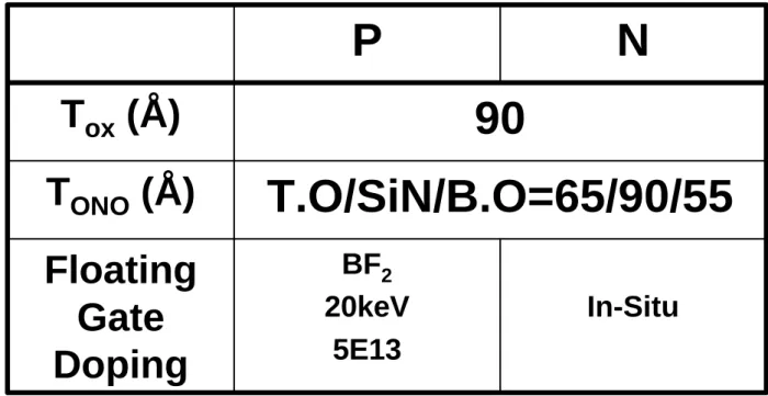
In this work, the flash memory cells are prepared based on standard 0.35µm CMOS process and with conventional stacked-gate flash memory cell. The cell sizes which we used in this study are W/L = 0.7/0.65 µm and 0.7/0.45 µm respectively. The floating gate width WFG = 1.2 µm, tunnel oxide thickness TOX = 90 Å, and effective ONO inter-poly dielectric
thickness TONO = 165 Å (The individual thickness of interpoly ONO is TTop-Oxide/ TSiN/
TBottom-Oxide=65Å/90Å/55 Å). Interpoly dielectric thickness heavily influences program/erase
Substrate
ONO
Tunnel Oxide
S
D
Substrate
LOCOS
Floating Gate
Control Gate
(b)
(c)
Floating
Gate
Control
Gate
Source
Drain
Width
Length
(a)
EC
Substrate
ONO
Tunnel Oxide
S
D
Substrate
LOCOS
Floating Gate
Control Gate
(b)
(c)
Floating
Gate
Control
Gate
Source
Drain
Width
Length
(a)
EC
Floating
Gate
Control
Gate
Source
Drain
Width
Length
(a)
EC
Fig. 2.1 Sketch and cross-sectional view of stacked-gate flash memory. (a) Layout of experimental stacked-gate flash memory. (b) The cross-sectional view of the flash cell in the length direction. (c) The cross-sectional view of the flash cell in the width direction.
(Medium Doped Drain) is used for applying the asymmetric electric field. There are two different doping types of floating gate. The detailed device parameters are summarized in Table 2.1.
2.2 Experimental Setup
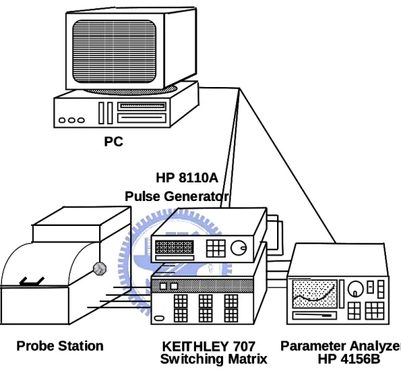
The experimental setup for the I-V and transient characteristics measurement of flash memory is illustrated in Fig. 2.2. Based on the PC controlled instrument environment via HP-IB (GP-IB, IEEE-488 Standard) interface, the complicated and long-term characterization procedures during analyzing the intrinsic and degradation behaviors in flash memory cells can be easily achieved. As shown in Fig. 2.2, the characterization equipments, including semiconductor parameter analyzer (HP 4156C), dual channels pulse generator (HP 8110A), low leakage switch mainframe (HP5250A Switching Matrix), and a probe station, provide an adequate capability for measuring the device I-V characteristics and carrying out the flash cell program/erase operations.
The HP 4156C is equipped with four programmable source/monitor units, two source units, and two monitor units for supplying or monitoring the voltage and the current. It provides a high current resolution up to pico-ampere range which facilitates the very low current measurement such as gate current measurement, subthreshold characteristics extraction, DCIV and GIDL measurement for oxide damage characterization. The dual channels HP 8110A with high timing resolution provides two different pulse levels simultaneously for transient and P/E cycling endurance characterization. The Switching Matrix, which is equipped with an 8-input x 12-outoupt switching matrix (with one output module), switches the signals from the HP 4156B and the HP 8110A to device under test (DUT) in probe station, automatically. In addition, the computer language-HP VEE is used to achieve the PC control of these measurement instruments via HP-IB interface.
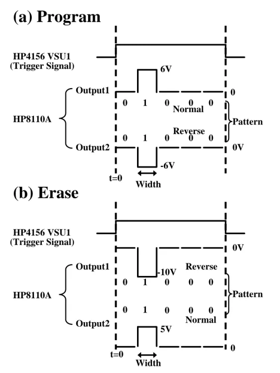
In order to precisely control the pulse timing of HP 8110A during transient and P/E cycling endurance characterization, we select the triggered pattern mode to achieve this requirement. Fig. 2.3 (a) and Fig. 2.3 (b) show the timing diagrams of the triggered pattern mode method during program and erase operations, respectively. By taking the program timing diagram as an example, the triggered pattern mode method can be explained as follows. In Fig. Fig. 2.3 (a), the VSMU1 of HP 4156B (illustrated in Fig. 2.2) generates a voltage signal which is equal to the low voltage of HP 8110A. This approach can provide a substrate bias during programming and prevent additional stress to device during programming. The patterned pulses (defined as 01000 in Fig. 2.3 (a) with the minimum period of 10ns) from HP 8110A are then sent and programming of a flash memory cell is performed. In our experience with the HP 8110A, we must set the period of pulse larger than 50 ~ 100ns to obtain a good square pulse and the leading or trailing edge larger than 25 to 50 ns to prevent the over-shoot and under-shoot of output pulse.
In-Situ
BF
220keV
5E13
Floating
Gate
Doping
T.O/SiN/B.O=65/90/55
T
ONO
(Å)
90
T
ox
(Å)
N
P
HP 8110A Pulse Generator
Probe Station
Switching Matrix KEITHLEY 707
Parameter Analyzer HP 4156B PC HP 8110A Pulse Generator Probe Station
Switching Matrix KEITHLEY 707
Parameter Analyzer HP 4156B PC HP 8110A Pulse Generator Probe Station
Switching Matrix KEITHLEY 707
Parameter Analyzer HP 4156B PC
Fig. 2.2 The experimental setup of the current-voltage and the transient characteristics measurement in flash cells. Automatic controlled characterizations system is setup based on the PC controlled instrument environment.
Width 0 6V 0V -6V
(a) Program
0 1 0 0 0 Output1 Output2 HP8110A HP4156 VSU1 (Trigger Signal) Pattern 0 1 0 Reverse0 0 Normal 0 5V(b) Erase
0 1 0 0 0 Output1 Output2 HP8110A HP4156 VSU1 (Trigger Signal) Normal Width 0V -10V 0 1 0 0 0 Reverse Pattern t=0 t=0Fig. 2.3 The timing diagram of the trigged pattern mode method during (a) program and (b) erase operation.
Chapter 3
Basic I-V Characteristics and Capacitance Coupling
Model of P-channel Flash Memories
This Chapter involves the extraction of MOSFET device basic parameters, threshold voltage, and the coupling model of floating gate memories to extract the parameter. Finally, we show the basic I-V Measurement of flash cells and dummy cells.
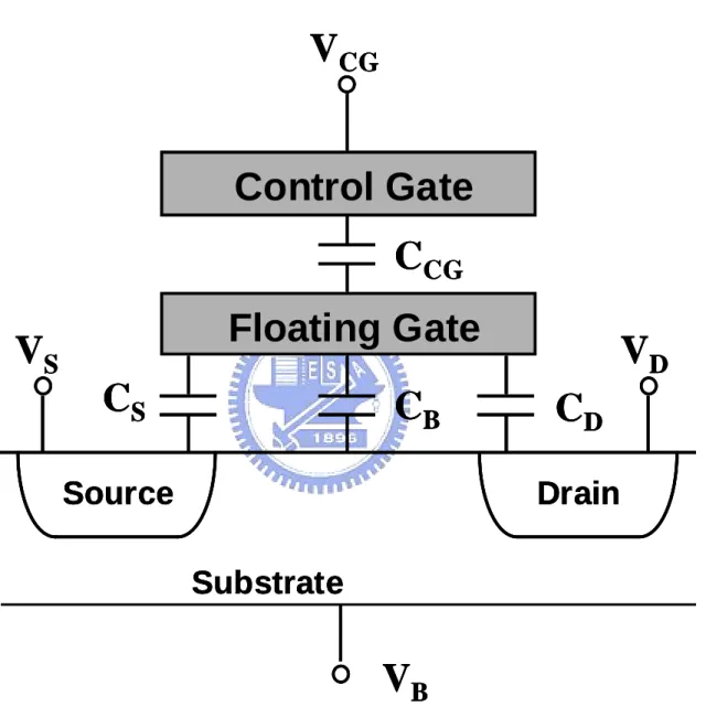
In floating gate memory, the floating gate is fully isolated. The voltage of floating gate (VFG) is determined by the coupling of the voltages of other terminals (Control-Gate,
Substrate, Source and Drain). Usually, the flash memory cell is modeled by a capacitance equivalent circuit, called the capacitance model [9] [10]. Based on this model, the equation of floating-gate voltage can be determined, from which we can extract the coupling ratio.
3.1 Threshold Voltage Determination
In this study, the threshold voltage VTH is determined from its ID-VG characteristic.
Based on the following drain current equation [11]: D TH GS ox ox D0 (V -V )V t L W I = µ ε , (3.1)
in which we can choose an arbitrary drain current level, and set the gate voltage at this drain current level as the device threshold voltage. However, by taking the device geometry into consideration, we need to normalize the device drain current with its channel length and width. This can be done by transforming Eq. (3.1) into
D TH GS ox ox D0 D (V -V )V t ) L W )/( (I I = =µε . (3.2)
Here, we set the threshold voltage as the gate voltage at which the normalized current (ID0) is
0.1µA.
3.2 Capacitance Model and Extraction of Coupling Ratio
It is required for an accurate prediction of the associated coupling ratio in the design of the flash memory cell. We will describe how to extract these parameters in this section. Besides, we will derive the equations for calculating the floating gate potential.
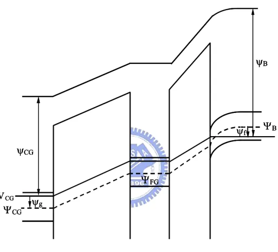
Fig. 3.1 shows the conventional capacitance model for the flash memory cell. According to this model, the charge balance of floating gate can be derived based on the electrostatic potential Ψ in the various regions of the cell. From
Fig. 3.2, we know that the electrostatic potential Ψ equals to (V+ψ) where V is applied voltage and ψ is flat-band voltage for each terminal, respectively. However, the electrostatic potential ΨFG of floating gate is equal to the voltage VFG. Therefore, the floating gate voltage
can be expressed as the following equation
TOTAL FG S FG S D FG D B FG B CG FG CG FG C Q ) (V ) (V ) (V ) (V V =α −ψ +α −ψ +α −ψ +α −ψ − (3.3) where S D B CG TOTAL C C C C C = + + + (3.4) and TOTAL X X C C = α . (3.5)
source coupling coefficient, and αD is the drain coupling coefficient. Then we assume
(αCGψCG+ αBψB+ αSψS+ αDψD) = V0 ≒ αCGψCG = VFB, which is the flat-band voltage of the
flash memory cell, and VB = 0 as the reference by setting VS and QFG to zero, the floating gate
voltage cab be rewritten as FB D D CG CG FG V V V V =α +α + . (3.6)
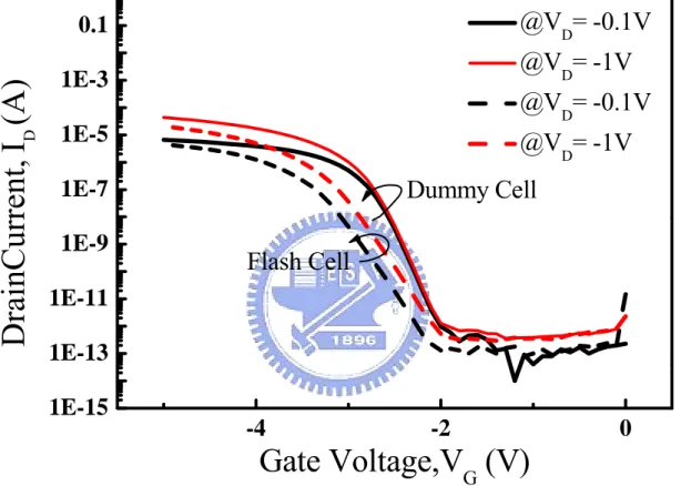
The coupling coefficients will be determined in Eq. (3.6). Fig. 3.3 shows the subthreshold characteristics of flash and dummy cells at drain voltage of 0.1 and 1V. Dummy cells show the identical subthreshold characteristic but flash cells are different. This is because the effect of coupling between electrodes. By selecting any two different drain current level (such as IDS
= 10-5 and 10-6 A) at VDS = 0.1V, the control gate coupling coefficient can be obtained as
A) 10 (I V -A) 10 (I V A) 10 (I V -A) 10 (I V 6 -DS CG 5 -DS CG -6 DS FG -5 DS FG CG = = = = = α . (3.7)
Since αCG is determined from Eq. (3.7), the value of VFB can also be determined from VFG-
αCGVCG at any fixed drain current level of VDS = - 0.1V.
3.3 GIDL Measurement
Gate Induced Drain Leakage Current (GIDL) is one of the major approaches to detect the damage of the oxide and silicon interface in the gate-drain overlap region. [12] [17]. The GIDL current is due to direct band-to-band tunneling in the Off-state MOSFETs. For flash memories, the effect of Band-to-Band tunneling can be also used to inject charges into floating gate [5]. Please refer to section 4.2 for the detailed description of Band-to-Band tunneling.
Fig. 3.4 Shows the GIDL measurements of P-channel flash and dummy cells. For flash cells, the more negative drain voltage causes electrons to be injected into floating gate via Band-to-Band tunneling and then gives rise to the threshold voltage shifts.
The GIDL current is sensitive to trapped charge in the tunneling oxide at the overlap region between the gate and drain, so that we can monitor the qualitative or the quantitative analysis of these Qox and Nit. The analytic model of the GIDL current [18] is shown as
follows: ) E B exp( E A I surface surface GIDL = × × − (3.8)
where Esurface is the electric field at silicon interface. The parameters A and B are defined in
Control Gate
Floating Gate
C
CG
C
B
C
D
C
S
V
CG
V
D
Source
Drain
V
S
V
B
Substrate
Control Gate
Floating Gate
C
CG
C
B
C
D
C
S
V
CG
V
D
Source
Drain
V
S
V
B
Substrate
Control Gate
Floating Gate
C
CG
C
B
C
D
C
S
V
CG
V
D
Source
Drain
V
S
V
B
Substrate
Ψ
Bψ
BΨ
CGΨ
FGψ
CGψ
g VCGψ
fΨ
Bψ
BΨ
CGΨ
FGψ
CGψ
g VCGψ
fΨ
Ψ
BBψ
Bψ
BΨ
CGΨ
CGΨ
FGΨ
FGψ
CGψ
CGψ
gψ
g VCG VCGψ
fψ
fFig. 3.2 Energy band diagram of a flash cell at the onset of inversion (with no charge in the floating gate).
-4
-2
0
1E-15
1E-13
1E-11
1E-9
1E-7
1E-5
1E-3
0.1
Flash Cell
Dummy Cell
@V
D= -0.1V
@V
D= -1V
@V
D= -0.1V
@V
D= -1V
DrainCurrent,
I
D(A)
Gate Voltage,V
G(V)
Fig. 3.3 The subthreshold characteristic of p-channel flash cell and dummy cell with different drain voltages.
-6 -4 -2 0 2 4 6 10-13 10-11 10-9 10-7 10-5 10-3 10-1
GIDL
Dummy Cell
W/L= 0.7/0.45
V
D= -2V
V
D= -4V
Dra
in
Current
, I
D(A)
Gate Voltage, VG (V) -6 -4 -2 0 2 4 6 10-14 10-12 10-10 10-8 10-6 10-4 10-2V
thshift
GIDL
V
D= -2V
V
D= -4V
Flash Cell
W/L= 0.7/0.45
Drain
Cur
ren
t, I
D(A)
Gate Voltage, VG (V)Fig. 3.4 GIDL current of (a) dummy cell and (b) flash cell in p-channel cells. For flash cells, the more negative drain voltage causes electrons inject into floating gate by Band-to-Band tunneling so the threshold voltage shifts.
(a)
Chapter 4
Mechanism and Characteristics of Forward Bias
Assisted Drain Hot Electron Injection
4.1 Introduction
In this chapter, first we describe the mechanism of familiar program schemes used in p-channel flash cells, Band-to-Band tunneling Hot Electron Injection (BBHE), and Drain Avalanche Hot Electron Injection (DAHE). Then, we propose a new program scheme called Forward Bias Assisted Drain Hot Electron Injection (FBADHE). We will investigate the mechanism and the effect on different programming conditions. Finally, we compare the characteristics of the above programming schemes.
4.2 Mechanism of BBHE and DAHE in P-channel Flash cells
In the past, BBHE and DAHE are the popular methods used for programming in P-channel Flash cells. In this section, we will investigate the difference of mechanism between them.
First, we discuss Band-to-Band tunneling Hot Electron Injection [5]. BBHE is used in P-channel Flash cells. For n-channel cells, if we change the structure of MOSFET, i.e., buried a p+ region in the channel, BBHE can also be achieved [7].
When a negative drain voltage and a positive control-gate voltage are applied, the energy band is bended by the difference of the two side of the insulator and band-to-band tunneling
tunneling means that: in the strong band bending, electrons in the valence band edge can move to conduction band, and holes are left on the valence band so that electron-hole pairs generate. Generated carriers will be accelerated by the horizontal electric field and some of them gain sufficient energy. The energetic electrons then inject into floating gate by the effect of vertical field. Fig. 4.1 shows the schematic illustration and the band diagram of BBHE.
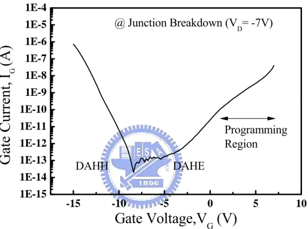
Drain Junction avalanche hot carrier (DAHC) historically denotes the emission of free carriers towards the gate generated by impact ionization in the deep depletion region of p-n junction. In p-channel flash cells, when a large negative drain voltage is applied and substrate is grounded, the drain-substrate p-n junction is in strong reverse-bias, the avalanche breakdown occurs. Electrons with high energy cause more and more impact ionization when moving from p region to n region and generate a large amount of electron-hole pairs. Carriers are accelerated by the strong electric field in depletion region so that the energy of these carriers is high enough to surmount the oxide barrier and inject into floating gate even without the assistance of vertical electric field. Fig. 4.2 shows the illustration and band diagram of DAHE. Vertical field determines which carrier will be injected. We measure the relationship of gate voltage and gate current at the condition of drain avalanche breakdown, as shown in Fig. 4.3. We can easily appear that only in the strong negative gate bias is applied (~-8V) that hot holes will inject into floating gate. In other condition, electron current is dominated. So the DAHE Programming Scheme is easily to be achieved in p-channel flash cells. DAHE is a high speed, self-convergent programming scheme [20]. Besides, if a positive gate voltage and a strong drain voltage are applied, a large electric field is generated in the gate-drain overlap region. Band-to-Band tunneling will occurs and electron will inject into floating gate. It is called Gate Induced Drain Leakage (GIDL) current [12].
From the above description, it is realized that the mechanism of BBHE and DAHE is quite different. First, the generation region of carriers (electron-hole pair) of BBHE is in the gate-drain overlap region, and the DAHE is in the deep depletion region of drain-substrate
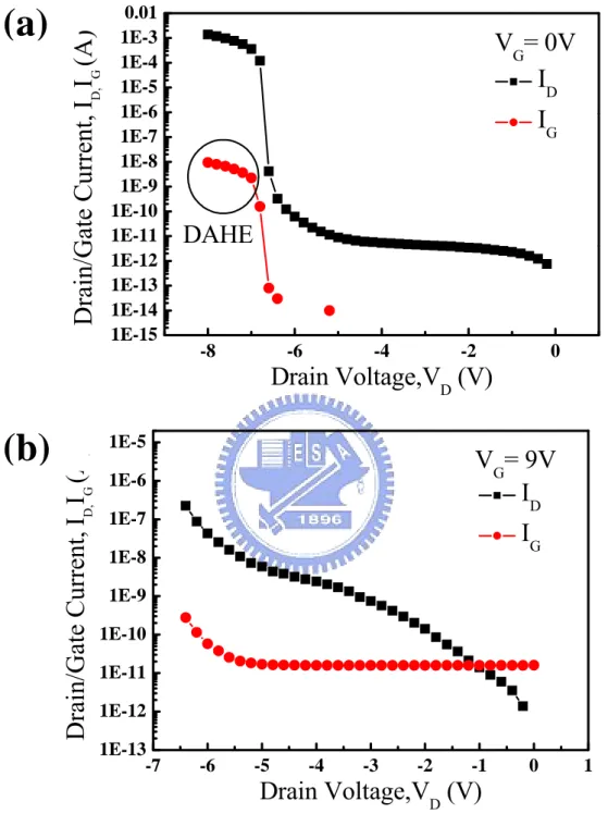
junction. Second, the energy of generated carriers of BBHE is lower than those in DAHE. Thus the stronger vertical field is needed for BBHE in order to surmount the oxide barrier. The advantage of BBHE is high injection efficiency (IG/ID). Fig. 4.4 shows the relationship of
IG, ID and VD under the BBHE and DAHE condition respectively. In Fig. 4.4 (a), the Gate
current rises at the drain junction breakdown (~-7V). It is realized as DAHE injection. In Fig. 4.4 (b), the Gate current involves F-N tunneling current and band-to-band tunneling current. The Gate current rises as the increasing of band bending. Because the F-N tunneling current is fixed, the increasing part is band-to-band tunneling current. Fig. 4.5 shows the injection efficiency (IG/ID) of BBHE and DAHE. The efficiency of BBHE (~10-3) is high than DAHE
(~10-7). It is noticed that in the injection efficiency has a maximum at VD= 0V. It is because
there is a little tunneling current (~10-11@ VG= 10V) but no drain current (~10-13@ VG= 10V).
So, the magnitude of gate and drain current should be also notified when measuring the injection efficiency. The higher efficiency means the less power consumption. It is noticed than the definition of injection efficiency (IG/ID). For CHEI Programming in N-Channel Flash
cells, The MOS is turned on, so the ID is drain current. On the other hand, using either BBHE
or DAHE on p-channel flash cells, the MOS isn’t turn on, so the ID is drain leakagecurrent.
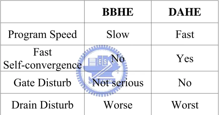
The other advantage of BBHE is the better drain disturb characteristics. The serious problem in reliability of p-channel flash is drain disturb [21], which impedes its practical applications for mass production purpose. Larger drain voltage causes more serious drain disturbance. The comparison of BBHE and DAHE is listed in Table 4.1.
P
+
Drain (-)
FG (+)
BTBT
D (P
+
)
Band-to-Band
tunneling
e
-
:
h
+
:
FG
Fig. 4.1 Schematic illustration and Band Diagram of BBHE on the p-channel flash cells. Electrons in the valence band edge can move to conduction band, and holes are left on the valence band so that electron-hole pairs generate.
Impact
Ionization
To FG
P
+Drain (-)
N Substrate (+)
D (P
+)
Impact Ionization
FG
Depletion region
e
-:
h
+:
Fig. 4.2 Schematic illustration and band diagram of DAHE on the p-channel flash cells. Electrons with high energy cause more and more impact ionization when moving from p (Drain) region to n (Substrate) region and generate a large amount of electron-hole pairs.
-15
-10
-5
0
5
10
1E-15
1E-14
1E-13
1E-12
1E-11
1E-10
1E-9
1E-8
1E-7
1E-6
1E-5
1E-4
Programming
Region
@ Junction Breakdown (V
D= -7V)
DAHE
DAHH
Ga
te C
urrent,
I
G(A
)
Gate Voltage,V
G(V)
Fig. 4.3 The relationship of gate voltage and gate current under the condition of drain junction breakdown on p-channel flash cells.
-8 -6 -4 -2 0 1E-15 1E-14 1E-13 1E-12 1E-11 1E-10 1E-9 1E-8 1E-7 1E-6 1E-5 1E-4 1E-3 0.01
DAHE
V
G= 0V
I
DI
GDrain/Gate Current,
I
D,I
G(A
)
Drain Voltage,V
D(V)
-7 -6 -5 -4 -3 -2 -1 0 1 1E-13 1E-12 1E-11 1E-10 1E-9 1E-8 1E-7 1E-6 1E-5I
DI
GV
G= 9V
Dr
ai
n/
Gat
e Cur
rent,
I
D,I
G(A)
Drain Voltage,V
D(V)
Fig. 4.4 The relationship of drain current, gate current and drain voltage under different gate voltage ((a) VG= 0V and (b) 9V respectively).
(a)
-8
-6
-4
-2
0
1E-8
1E-6
1E-4
0.01
1
100
DAHE
BBHE
V
G= 0V
V
G= 10V
Injection E
fficiency,
I
G/
I
D(A)
Drain Voltage,V
D(V)
Fig. 4.5 Injection efficiency (IG/ID) with different gate voltages. The injection efficiency of
BBHE DAHE
Program Speed
Slow
Fast
Fast
Self-convergence
No Yes
Gate Disturb
Not serious
No
Drain Disturb
Worse
Worst
4.3 Mechanism of Forward Bias Assisted Drain Hot Electron Injection in
N-Channel Flash Cell
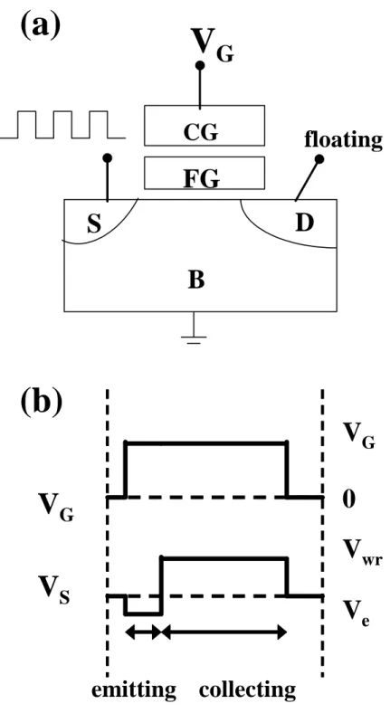
The concept of forward bias assisted programming is proposed by Z. Liu in 1999 [13]. The sample is N-Channel floating gate cells. This program scheme is called “Pulse Agitated Substrate Hot Electron Injection” (PASHEI). The illustration of Program setup is shown in Fig. 4.6. The programming pulse is divided into two parts, emitting time and collect time. The emitting is used to make the substrate-drain diode in forward bias (a negative drain voltage Ve
is applied) and the diffusing current is taking place. Then, changing the diode to reverse bias mode (a positive drain voltage Vwr is applied), and the electrons which are flowing into
substrate will be injected into floating gate. The gate voltage VG keeps positive during
emitting and collecting time. Please refer to Fig. 4.7 for the injection mechanism. The advantage of this programming technique is only a small programming voltage (~5V as gate voltage and 4V as drain writing voltage) is needed. The disadvantage is a multiple pulse is needed in a program procedure, such as: 100 pulse per programming. It makes the long period of programming time and a complicated circuit design is needed in order to apply this continuous pulse.
We modify the pulse pattern in this study. As shown in Fig. 4.8. We call the new scheme “Forward Bias Assisted Substrate Electron Injection” (FBASEI). The difference is that the gate voltage is zero during the emitting period and is positive during collecting period. The mechanism is similar as PASHEI, so the injection current is from the substrate too. The performance comparison of CHE, PASHEI and FBASEI is shown in Fig. 4.9. The characteristic of FBASEI is also pulse count dependent, pulse period independent, and low operating voltage is achieved [13]. The reason of poorer programming speed of FBASEI (comparing with PASHEI) is that the less gate pulse period makes fewer electrons injected into the floating gate.
0
V
Gemitting
collecting
floating
S
D
FG
CG
V
G
V
G
B
V
S
(b)
V
wrV
e(a)
-D (n+)
(b) V
D=V
e=-1
h
+e
-D (n+)
(c)V
D=V
wr=6
e
-+
D (n+)
(a) V
D=0
B (p)
Fig. 4.7 The injection mechanism of PASHEI in n-channel flash cells. Substrate electron current inject to floating gate by the effect of vertical electric field.
floating
S
D
FG
CG
V
G
B
(b)
(a)
0
V
Gemitting
collecting
V
G
V
S
V
D-HighV
D-LowFig. 4.8 The programming setup and pulse pattern of FBASEI in n-channel flash cells. The substrate (p)-drain (n) diode in emitting period is in forward bias and is in reverse bias in collecting time.
1E-7
1E-6
1E-5
1E-4
1.0
1.5
2.0
2.5
3.0
3.5
4.0
CHE
PASHEI
FBASEI
Threshold Voltage, V
th(V)
Program Time (sec)
Fig. 4.9 The characteristics of transient program of CHE, PASHEI and FBASEI in n-channel flash cells.
4.4 Mechanism of Forward Bias Assisted Drain Hot Electron Injection in
P-channel Flash Cell
In this section, we will first discuss the difference of mechanism of forward bias assisted hot electron injection in P and N Channel cells. Second, we define the gate current components under different program schemes. Finally, we compare the characteristics with the assistance of forward bias at different operation conditions.
The injection mechanism and performance of the forward bias assisted programming scheme in P-channel cells is quite different from the in N-Channel cells. Fig. 4.10 (a) shows the programming setup and pulse pattern of this program scheme. The concept is similar to N-Channel ones. First, a moderate positive bias is applied on the P-type drain side, and the junction is under forward bias. When changing the mode to reverse bias, deep depletion region is created and carriers in this region suffer strong electric field. Impact Ionization occurs and much energetic carrier is generated and injected into the floating gate. Please refer to Fig. 4.10 (b) for the detailed mechanism. The difference of the scheme in N-Channel ones is the carrier generated in the drain depletion region, so it is Drain Electron Injection and can be called Forward Bias Assisted Drain Hot Electron Injection (FBADHE).
Fig. 4.11 shows the operational region (the combination of gate voltage and drain voltage) with different programming schemes. Before discussing the injection mechanism of the above schemes, we should first clearly define the regions of breakdown, sub-breakdown and Band-to-Band tunneling region. The I-V characteristic of drain-substrate diode is shown in Fig. 4.12. When the drain voltage is larger than 0.7V, the junction is in forward bias (drain current >0); on the contrary, when the drain voltage is below than 0.7V, the junction is in reverse bias (drain current <0). Significant reverse bias leakage current rises as VD= -5.5V
(~10-11 A), and increases rapidly to ~10-4 A at VD= -7V. The point (I) (VD= -5.5V) is called
p-side valance band to n-side conduction band [23]. The point (II) (VD= -7V) is avalanche
breakdown. It is due to impact ionization induced generated electron-hole pair. The original and generated electrons are both swept to the n side of the junction, and the holes are swept to the p-side [23]. The drain voltage in FBADHE (~6V) is between (I) and (II), both breakdown mechanism may also occur. Avalanche breakdown is the main breakdown mechanism in p-n junction [24], so in this region, we believe the avalanche breakdown dominates. In the following description of this thesis, we call this region sub-breakdown region. It is noted that the breakdown voltage is related to the doping concentration of the drain and substrate.
Next, we discuss the mechanism of injected electrons in different operational conditions. In FN-PGM regions, of course the injected current is F-N tunneling current; If the device operates in the Band-to-Band tunneling region (i.e. VG-VD= 15V, VD= -5V, VG= 10V), the
Band-to-Band tunneling current dominates; If the device operates in the drain avalanche breakdown condition (i.e. VD = -7V and VG= 0V), the injection charge is drain avalanche
induced hot electrons.
The drain leakage current at VG= 0V and VD in sub-breakdown region in MOSFETs is
realized as Band-to-Band tunneling current from the gate-drain overlap region [12] [19]. But in flash EEPROMs, the thicker oxide makes the Band-to-Band tunneling current injection at zero gate voltage impossible. So the applied voltage must be adjusted, i.e., applying an appropriate gate voltage to achieve enough band bending. Furthermore, if we operate the device in the sub-breakdown region plus a small gate voltage (i.e. VD = -6V and VG= 6V), the
composition of gate current is more complicated. The amount of drain breakdown (involves Zener breakdown and avalanche breakdown and avalanche breakdown dominates) induced carriers in sub-breakdown region is small but some of them may gain sufficient energy from vertical field. Besides, with the influence of vertical electric field caused by the positive gate voltage, the potential difference between gate and drain is large enough to induce more Band-To-Band Tunneling current. Thus, the injection charge will involve drain avalanche
induced hot electrons current and Band-To-Band Tunneling current.
It is hard to separate the gate current components in different operational conditions accurately by measurement only because the current component substantially changes as the change of the combination of the drain voltage and gate voltage. Fig. 4.13 shows the relationship of gate current and drain current in p-channel dummy cells. By varying the value of gate voltage, we can roughly separate the gate current components. The gate current difference between VG= 0V and VG= 9V at VD= 0V is F-N tunneling current. The triangle line
(VG= 9V) rises as VD= 5.5V is due to Band-to-Band tunneling. The square line (VG= 0V)
rises sharply at VD= 7V is drain avalanche breakdown current. The gate current of circle line
(VG= 5V) rises at VD= 5V is initially Band-to-Band tunneling current. And then as the
increasing of drain voltage (to ~6V), some of the avalanche breakdown induced electrons gain enough energy from vertical field and become a part of gate current.
Another simple method to determine the gate current components is shown in Fig. 4.14. The potential difference of gate and drain is fixed as 12V (solid circle) and 7V (hollow circle) respectively. It represents the band bending is the same at the whole line so that the amount of injection carrier due to BBHE is the identical. It helps us to find the other gate current components with different combinations of gate/drain voltage. When the drain voltage is -2V, electron F-N tunneling current is the main component. At drain voltage equals to -6V, sub-DAHE generates, as previous description. At drain voltage equals to -7V, there is a lot carriers injecting due to drain avalanche breakdown. Besides, comparing the two spot at VD=
-7V, we can see the small gate voltage (5V) enhance the injection of electrons by an order. This is because the injection of Band-to-Band hot electrons and additional drain avalanche breakdown hot electrons.
self-convergent. So, in these 2 conditions the Drain Avalanche breakdown current is the main injection component. The injection component of BBHE is Band-To-Band Tunneling current. The threshold voltage of sub-breakdown B is almost fixed. This is because both the band bending and drain avalanche is not large enough to generate apparent injected current. The measurement result conforms to our explanation.
In summary, the injected gate current under sub-breakdown region is drain avalanche induced hot electrons and Band-To-Band tunneling current, and from Fig. 4.15, drain avalanche induced hot electrons is the main component.
Now we investigate the influence of the drain forward bias in the above operational regions. Table 4.2 shows the operational condition of P/E schemes in this study. Fig. 4.16 shows the original and forward-bias-assisted characteristics of transient program under different operating conditions. From this measurement, we clearly identify the mechanism of the assistance of forward bias. At BBHE (circle line), there is no difference after assistance of forward bias, this is because the forward bias doesn’t influence the Band-to-Band tunneling current. The performance with forward bias shows the emphatically difference on DAHE (square line) and sub-breakdown region (triangle line). This is because the forward bias makes more impact ionization at the Drain-Substrate junction so that more energetic carriers surmount the oxide barrier and inject into floating gate. This result is consistent with our proposal at the second paragraph of this section.
Since the assistance of forward bias works in drain avalanche breakdown and sub-breakdown region, considering the reliability issue: drain disturb, the larger drain bias during programming causes more serious drain disturb, so we select the sub-breakdown region as our operational condition in this thesis..
0
V
Gemitting
V
GV
DV
D-HighV
D-Lowcollecting
floating
S
D
FG
CG
V
G
B
V
D0
(1) V
D=0
D (p+) B (n)+
D (p+)(2) V
D=V
D-High= 1
h
+e
-D (p+)(3)V
D=V
D-High=-6
e
--Depletion region
Fig. 4.10 The (a) program setup, pattern mode and (b) injection mechanism of PASHEI in p-channel flash cells.
(a)
V
D
(-)
V
G
(+)
DAHE
BBHE
FN-PGM
Subbreakdown
Fig. 4.11 The combination of gate voltage and drain voltage of different programming schemes.
-8
-6
-4
-2
0
2
4
1E-14
1E-12
1E-10
1E-8
1E-6
1E-4
0.01
1
(II)
(I)
P-N Diode
Forward-Bias
Breakdown
Breakdown
Zener
Avalanche
I
D<0
I
D>0
D
rain Cur
rent,
|
I
D|
(A)
Drain Voltage, V
D(V)
-9
-8
-7
-6
-5
-4
-3
-2
-1
0
1
10
-1210
-1110
-1010
-910
-810
-7BBHE
BBHE+ DAHE
DAHE
F-N Tunneling
V
G= 0V
V
G= 5V
V
G= 9V
G
ate Curr
ent, I
G(A)
Drain Voltage, V
D(V)
Fig. 4.13 The IG-VD characteristics with different gate voltage in p-channel dummy cells.
From this figure, we can roughly separate the gate current components by the difference of gate voltage.
-7
-6
-5
-4
-3
-2
10
-1210
-1110
-1010
-910
-810
-7DAHE
Fixing Band Bending
V
G-V
D= 12V
V
G-V
D= 7V
Gate Current, I
G(A)
Drain Voltage, V
D(V)
DAHE
Sub-DAHE
F-N Tunneling
Fig. 4.14 The gate current components by fixing the potential difference between gate and drain terminal.
10
-710
-610
-510
-410
-3-5
-4
-3
-2
-1
0
1
2
3
BBHE (10/-5) Subbreakdown A(6/-6) DAHE (0/-7) Subbreakdown B(2/-6) Note: (VG/VD)Thres
hold Voltage,
V
th(V)
ProgramTime (sec)
Operate V
GV
DV
BV
SBBHE
11 -5 0
f
DAHE
0 -7 0
f
PGM
FBADHE
6
V
D-High=1
V
D-Low=~ -6*
0 f
ERS Channel-FN
-10 f 5
f
Read
-3 -1 0
0
10
-710
-610
-510
-410
-310
-2-5
-4
-3
-2
-1
0
1
2
Triangle:V
G= 6 V
D-Low= -6
Square: V
G= 0 V
D-Low= -7
V
D-High= 0
V
D-High= 1
Thres
hold Voltage, V
th(V)
ProgramTime (sec)
V
G= 10 V
D-Low= -5
Fig. 4.16 Transient program characteristics with the assistance of drain forward bias under different operating conditions.
4.5 Study of FBADHE at Sub-breakdown Region in P- Channel Flash Cell
In this section, we will investigate the characteristics of Forward Bias Assisted Drain Hot Electron Injection at sub-breakdown region. The related symbols are shown in Fig. 4.10 (a).
First, we discuss the dependence of drain emitting voltage (drain forward bias, VD-High),
as shown in Fig. 4.17 (a). The threshold voltage shift has a maximum at VD-High= 1V. It can be
explained that the large forward bias (> 1V) will increase the momentum of diffusing carriers and reduce the effect of impact ionization. Fig. 4.17 (b) shows the impact of the drain collecting voltage (drain reverse bias VD-Low). As predicted, the larger drain bias makes the
more threshold voltage shift. This is because the larger drain bias causes more impact ionization in the deep depletion region.
Fig. 4.18 shows the dependence of drain emitting time. We can find that there is no dependence of emitting time since the time to drive P-N diode in active area is very short (<1 μs). For convenience, we select emitting time =1μs on following measurement. The dependence of collecting time (pulse width) is shown in Fig. 4.19. This figure shows that the FBADHE is pulse width independent, because the same program time with different width shows the different result. The characteristic is different from other programming schemes, i.e., CHE, F-N and BBHE. Let me redraw this figure by replacing the X axis to programming pulse count, as shown in Fig. 4.20. We find that FBADHE is indeed pulse width dependent. This characteristic is due to a large amount of carriers are generated by the path of Sub-drain avalanche breakdown and Band-to-Band tunneling in a very short time (<1μs), and increasing the programming width is useless to enhance the amount of generated charges.
0.0 0.5 1.0 1.5 2.0 2.5 3.0 1.4 1.6 1.8 2.0 2.2 2.4 2.6 VG= 6V, VD-Low= -5.7V Pulse Width= 10us
Threshold Voltage s
hift,
∆
V
th(V)
Drain Forward Bias, V
D-High(V)
-5.8 -5.6 -5.4 -5.2 -5.0 0 1 2 3 4 5 6
V
G= 6V, V
D-High= 1V
Pulse Width= 10us
Threshold Voltage shift,
∆
V
th(V
)
Drain Reverse Bias, V
D-Low(V)
Fig. 4.17 The relationship of drain (a) forward bias (VD-High) and (b) reverse bias (VD-Low) on
10
-110
010
110
22.0
2.5
3.0
3.5
4.0
4.5
5.0
VG= 6V, VD-Low= -5.6V
Colleting Width= 1us
T
hres
hold Voltage shift,
∆
V
th(V
)
Emitting Time (us)
10
-710
-610
-510
-42
3
4
V
G= 6V
V
D-High= 1V
V
D-Low= -5.6V
Delta Threshold Voltage,
∆
V
th(V)
Program Time,(sec)
0
2
4
6
8
10
12
2.0
2.5
3.0
3.5
4.0
4.5
V
G= 6V
V
D-High= 1V
V
D-Low= -5.6V
Width= 20
µ
s
Width= 2
µ
s
Width= 0.1
µ
s
Delta Threshold Voltage,
∆
V
th(V)
Pulse Count
4.6 Erase Operation in P- Channel Flash Cell
The purpose of erase operation is to remove the electrons form floating gate to the device and reduce its threshold voltage. Folwer-Nordheim (F-N) tunneling is used to erase the flash cells. However, F-N operation requires high voltage across the tunnel oxide. Under strong electric field, electrons tunnel from floating gate and inject into channel or source region. This F-N tunneling effect is one of the main reliability issues in MOS devices, but is used to operate in flash devices.
Folwer-Norheim tunneling current occurs when the electric field crossing the tunnel oxide is large enough to make electrons whose energy is less than the barrier height can tunnel through the oxide to substrate. The F-N tunneling current IFN can be expressed as a
function of the electric field: 2 FN OX OX -B I α E exp( ) E (4.1) where B is a constant depending on effective mass and the barrier height.
There are two kinds of Folwer-Nordheim tunneling Erase scheme used in the flash cells: Channel F-N [14] [15] and edge F-N [1] [16]. The channel F-N is to remove the electrons uniformly from the whole channel, and the Edge F-N is from the source edge. For N-Channel cells, the negative Control Gate voltage and positive Substrate voltage is applied during Channel F-N; Control Gate grounded and positive Source voltage is applied during Edge F-N. The two erase techniques have their own advantage. The reliability of F-N Erase is hole injection into the tunnel oxide (Qox). Channel F-N Erase generates positive oxide charge in
the oxide above the channel and the Edge F-N erase will generate positive charge in the tunnel oxide. Qox will damage the oxide and cause the data loss of the memory cell [22].
electrons form floating gate. This is because the doping type of source (P) and substrate (n). In order to keep the diode in reverse bias, the potential of source must not be larger than substrate potential so edge F-N is unsuitable in P-channel cells. Fig. 4.21 shows the setup and band diagram of Channel F-N erase. Source and drain are floating during erase process. Fig. 4.22 shows the erase characteristic of P-channel Flash cells. Fig. 4.22 (a) indicates the larger electric field between the tunnel oxide causes more threshold voltage shift. Fig. 4.22 (b) indicates that the same electric field makes the same threshold voltage shift, whether the voltage is applied on gate or substrate.