國
立
交
通
大
學
電機與控制工程學系
碩
士
論
文
可適性調整相位邊限之電流回授補償技術
應用於無電容式低壓降線性穩壓器
Current Feedback Compensation Technique
for Adaptively Adjusting the Phase Margin
in Capacitor-Free LDO Regulators
研 究 生:楊奐箴
指導教授:陳科宏 博士
可適性調整相位邊限之電流回授補償技術
應用於無電容式低壓降線性穩壓器
Current Feedback Compensation Technique for Adaptively Adjusting
the Phase Margin in Capacitor-Free LDO Regulators
研 究 生:楊奐箴 Student:Huan-Chien Yang
指導教授:陳科宏
Advisor:Ke-Horng Chen
國 立 交 通 大 學
電 機 控 制 工 程 學 系
碩 士 論 文
A Thesis
Submitted to Department of Electrical and Control Engineering
College of Electrical Engineering
National Chiao Tung University
in partial Fulfillment of the Requirements
for the Degree of
Master
in
Electrical and Control Engineering
September 2007
Hsinchu, Taiwan, Republic of China
中華民國九十六年十二月
可適性調整相位邊限之電流回授補償技術
應用於無電容式低壓降線性穩壓器
研究生:楊奐箴
指導教授:陳科宏博士
國立交通大學電機與控制工程研究所碩士班
摘 要
隨著可攜式設備的蓬勃發展,為了有效使用分配有限的電池能量,電源管理系統是 不可或缺的一環。低壓降線性穩壓器具有架構簡單、低雜訊、低成本的優點,對於電源 管理晶片系統來說,低壓降線性穩壓器是一個非常重要而且廣泛應用的單元。 傳統低壓降線性穩壓器利用外部電容串聯寄生電阻補償,然而增益及極點位置隨負 載變動,使得寄生電阻補償方式更顯得複雜。近年來,對於高效能(高精準度、高電源 排斥比)之線性穩壓器需求越來越大,多級放大器之線性穩壓器恰可達到這個需求。同 時,隨著系統單晶片的發展,無電容式之線性穩壓器逐漸受到重視。由於不需要外掛電 容,電路板面積可大幅縮減,成本也大為降低。然而多級放大器之線性穩壓器的缺點是 有最低負載的限制,導致無載時的功率耗費。 本論文將提出一可適性調整相位邊限之電流回授補償技術應用於無電容式低壓降 線性穩壓器,此電流回授補償技術可可適性調整相位邊限在 60°左右以達到快速之暫態 反應能力。同時,在不犧牲頻寬之情況下,最低負載限制大幅降低至 50µA。此外,電 流回授補償技術使用與品質因素降低技術相當的補償電容,但電流回授補償技術可維持 高的電源排斥能力頻寬。本論文使用 TSMC 0.35µm2P4M 製程,補償電容僅需 5pF 以及 1.5pF。實驗結果顯示,最低負載限制大幅降低至 50µA,而具可適性相位控制之低壓降 線性穩壓器之暫態反應時間小於 4µs。Current Feedback Compensation Technique for Adaptively Adjusting
the Phase Margin in Capacitor-Free LDO Regulators
Student: Huan-Chien Yang Advisor: Dr. Ke-Horng Chen
Department of Electrical and Control Engineering
National Chiao-Tung University
Abstract
With the increasing demanding of portable devices, how to use the battery energy efficiently is the most concerned problem. Therefore, power management system is indispensable for modern consumer products. For power management system, low-dropout (LDO) liner regulator is the most common block due to the characteristics, such as simplicity, small board space, low noise and cost.
Conventional LDO regulator is compensated by the equivalent series resistor (ESR). However, this kind compensation is hardly to maintain because gain and poles locations are varied with load conditions. In recent years, the demanding for high performance liner regulator such as high load regulation and high power supply rejection is getting growing. The Multi-stage LDO can achieve this target. Meanwhile, with the development of SoC system, a capacitor-free LDO is preferred to reduce the board space and cost greatly. However, the most important disadvantage of multi-stage LDO is the minimum load restriction.
Therefore, a current feedback compensation (CFC) technique for capacitor-free LDO regulators with adaptively adjusting the phase margin is proposed in this thesis. CFC technique can adaptively adjust the phase margin for achieving better transient response than that with variant phase margin at different load current conditions. Not only fast transient response is attained due to suitable phase margin but also the minimum load current limitation can be greatly reduced to about 50µA without sacrificing bandwidth at light load current condition. Besides, CFC technique can have high PSRR bandwidth with compatible compensation capacitors compared to the Q-reduction technique. The capacitor-free LDO regulator with CFC technique is fabricated by TSMC 0.35µm 2P4M CMOS process with small compensation capacitors 5pF and 1.5pF. Experimental results demonstrate that the minimum load can be reduced to 50µA and transient response time with adaptively phase margin control is smaller than 4µs.
誌
誌
誌
誌
謝
謝
謝
謝
對於能夠順利拿到碩士學位,必須要感謝非常多的人。首先,必須要感謝我的指導 教授陳科宏博士對於我兩年來的指導,陳老師提供完整的實驗室資源以及研究上的指 導,使得碩士研究生涯豐富精進不少。再者必須感謝我的父母以及家人對我的用心栽 培,得以讓我在研究生活上無後顧之憂。最後,必須感謝實驗室學長姐們,同學劉玓玓、 莊詠竣以及林立家,還有許多大學的死黨們,和學弟們在課業上以及生活上互相的幫忙 以及照顧。 謹以這篇論文獻給所有幫助過以及關心過我的人。 謝謝。 楊奐箴 國立交通大學 中華民國九十六年十二月
Contents
CHAPTER 1 ... 1
INTRODUCTION ... 1
1.1POWER MANAGEMENT SYSTEM ... 1
1.2INTRODUCTION TO DIFFERENT REGULATORS ... 3
1.2.1 Linear Regulator ... 3
1.2.2 Switching Converter ... 4
1.2.3 Charge Pump ... 5
1.2.4 Comparison ... 6
1.3IMPORTANCE OF LINEAR REGULATOR ... 6
1.4MOTIVATION ... 8
CHAPTER 2 ... 9
CONVENTION AL AND PROPOSED LDO REGULATORS ... 9
2.1DEFINITIONS OF LDOREGULATOR ... 9
2.1.1 Dropout Voltage ... 10
2.1.2 Efficiency... 11
2.1.3 Transient Response ... 11
2.1.4 Line & Load Regulation ... 15
2.1.5 Power Supply Rejection (PSR) ... 16
2.1.6 Accuracy ... 19
2.2CONVENTIONAL LDOREGULATORS ... 19
2.2.1 Types of Pass Device ... 19
2.2.2 Conventional LDO Regulators ... 21
2.3PROPOSED LDOREGULATORS ... 23
2.3.1 Miller Compensation ... 23
2.3.2 Insert a Buffer Stage ... 24
2.4MULTI-STAGE LDOREGULATORS ... 25
2.4.1 Three-Stage LDO with Pole-Splitting Compensation ... 26
2.4.2 Three-stage LDO with Damping-Factor-Control Compensation ... 31
2.4.3 Three-stage LDO with Q-Reduction Compensation ... 32
2.4.4 Equivalent Two-Stage LDO Design ... 34
CHAPTER 3 ... 36
3.1THREE-STAGE LDOREGULATOR WITH RESISTIVE LOAD AT SECOND STAGE ... 37
3.2CURRENT FEEDBACK COMPENSATION (CFC) FOR THREE-STAGE LDOREGULATOR ... 39
3.2.1 CFC Capacitor-Free LDO Regulators ... 40
3.2.1.1 CFC Capacitor-Free LDO under Ultra Light Load Condition with Smaller Rz ... 44
3.2.1.2 CFC Capacitor-Free LDO under Light to Medium Load Condition ... 47
3.2.1.3 CFC Capacitor-Free LDO under Heavy Load Condition with Larger Rz ... 48
3.2.1.4 Summary of CFC Capacitor-Free LDO Regulators ... 49
3.2.2 CFC LDO with an Off-Chip Capacitor ... 50
3.2.2.1 Off-Chip Capacitor Design under No Load Condition ... 52
3.2.2.3 Off-Chip Capacitor Design under Heavy Load Condition ... 54
3.3BANDGAP REFERENCE ... 56
CHAPTER 4 ... 58
CIRCUIT IMPLEMENTATIONS & SIMULATION RESULTS ... 58
4.1CIRCUIT IMPLEMENTATION &DESIGN ... 59
4.1.1 CFC LDO Regulator Structure ... 59
4.1.2 Bandgap Reference ... 66
4.1.3 Biasing Circuit ... 69
4.2SIMULATION RESULTS OF CFCLDOREGULATOR ... 70
4.3PERFORMANCE OF CFCLDOREGULATOR ... 75
CHAPTER 5 ... 77
MEASUREMENT RESULTS AND CONCLUSIONS ... 77
5.1MEASUREMENT METHODS AND RESULTS ... 77
5.1.1 Measurement Methods ... 78
5.1.2 Measurement Results ... 79
5.2CONCLUSIONS ... 81
5.3FUTURE WORK ... 82
Figure Captions
Fig. 1. Energy of chip requirement. ... 2
Fig. 2. Power management system. ... 3
Fig. 3. Linear regulator. ... 4
Fig. 4. Conventional voltage mode switching buck converter. ... 5
Fig. 5. Charge pump converter. ... 6
Fig. 6. Linear regulator served as pre-regulator... 7
Fig. 7. Linear regulator served as post-regulator. ... 7
Fig. 8. Definition of dropout voltage. ... 10
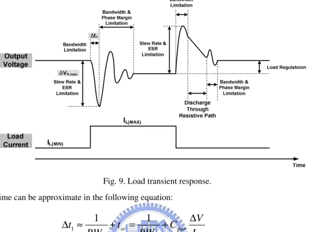
Fig. 9. Load transient response. ... 12
Fig. 10. Output drops during light to heavy load. ... 12
Fig. 11. Output drops during heavy to light load. ... 13
Fig. 12. Output discharge through resistive network. ... 14
Fig. 13. Line transient response. ... 14
Fig. 14. Definition of line regulation. ... 15
Fig. 15. Definition of load regulation. ... 16
Fig. 16. Approximate modeling of PSR. ... 17
Fig. 17. PSR frequency response. ... 18
Fig. 18. Types of pass device. ... 20
Fig. 19. Conventional LDO regulator. ... 21
Fig. 20. Difficulty of ESR compensation. ... 23
Fig. 21. Miller compensation technique for LDO regulators. ... 24
Fig. 22. Buffer stage for LDO regulator. ... 25
Fig. 23. Single Miller compensation for three-stage LDO regulator. ... 26
Fig. 24. Single Miller capacitor compensation for three-stage LDO regulator. ... 27
Fig. 25. Analysis structure of SMC LDO regulator. ... 28
Fig. 26. Small signal analysis of SMC LDO regulator. ... 29
Fig. 27. Pole-zero location of SMC LDO regulator. ... 30
Fig. 28. Magnitude peaking at light load condition. ... 30
Fig. 29. LDO with Damping-Factor-Control compensation. ... 31
Fig. 30. LDO with of Q-reduction compensation. ... 32
Fig. 31. Circuit level of LDO with Q-reduction compensation. ... 33
Fig. 32. PSR performance of Q-reduction compensation. ... 34
Fig. 33. Equivalent two-stage LDO regulator. ... 35
Fig. 34. Three-stage LDO with resistive load at second stage. ... 37
Fig. 36. Structure of CFC capacitor-free LDO regulator. ... 40
Fig. 37. Small signal analysis of CFC capacitor-free LDO regulator. ... 41
Fig. 38. Poles and zero locations of CFC LDO as load increased. ... 43
Fig. 39. Pole locations with CFC technique. ... 43
Fig. 40. CFC capacitor-free LDO under light load condition. ... 45
Fig. 41. Frequency response of CFC LDO simulated by MATLAB. ... 46
Fig. 42. Summarized poles and zero of CFC capacitor-Free LDO Regulators. ... 50
Fig. 43. Analysis structure of CFC LDO regulator with off-chip capacitor. ... 51
Fig. 44. Small signal analysis of CFC LDO regulator with off-chip capacitor. ... 51
Fig. 45. Frequency response of off-chip capacitor design under light load condition... 53
Fig. 46. Frequency response of off-chip capacitor design under heavy load condition. ... 54
Fig. 47. Variation of gate-source and gate-drain capacitances versus VGS. ... 55
Fig. 48. Conventional bandgap reference. ... 56
Fig. 49. Circuit schematic of CFC LDO regulator... 59
Fig. 50. Loop responses of CFC capacitor-free LDO under different load conditions. ... 62
Fig. 51. Loop responses with and without CFC technique. ... 63
Fig. 52. PSR performance of CFC capacitor-free LDO regulator. ... 64
Fig. 53. PSR performance with different compensation technique. ... 64
Fig. 54. Loop responses under different load conditions with off-chip capacitor. ... 65
Fig. 55. Circuit schematic of bandgap reference. ... 66
Fig. 56. Simulation of reference voltage at different supply voltages. ... 67
Fig. 57. Simulation of bandgap op amp. ... 67
Fig. 58. Simulation of PSR of bandgap reference. ... 68
Fig. 59. Circuit schematic of biasing circuit. ... 69
Fig. 60. Simulation of biasing current versus temperature and supply voltage. ... 70
Fig. 61. Load transient test method. ... 71
Fig. 62. Load transient of CFC capacitor-free LDO under light load to heavy load. ... 71
Fig. 63. Load transient of CFC capacitor-free LDO under heavy load to light load. ... 72
Fig. 64. Load transient of CFC LDO with off-chip capacitor. ... 73
Fig. 65. PSR performance of CFC capacitor-free LDO. ... 74
Fig. 66. PSR performance of CFC LDO with an off-chip capacitor. ... 74
Fig. 67. Layout of CFC LDO regulator. ... 76
Fig. 68. Die photograph of CFC LDO regulator. ... 77
Fig. 69. Load performance tests of CFC Capacitor-free LDO Regulator. ... 78
Fig. 70. Line performance tests of CFC Capacitor-free LDO Regulator. ... 78
Fig. 71. Measured load transient response from 50µA to 100mA at Vin 3V. ... 79
Fig. 72. Measured load transient response from 100mA to 50µA at Vin 3V. ... 79
Fig. 73. Measured line transient response from 3V to 5V at load current 100mA. ... 80
Table Captions
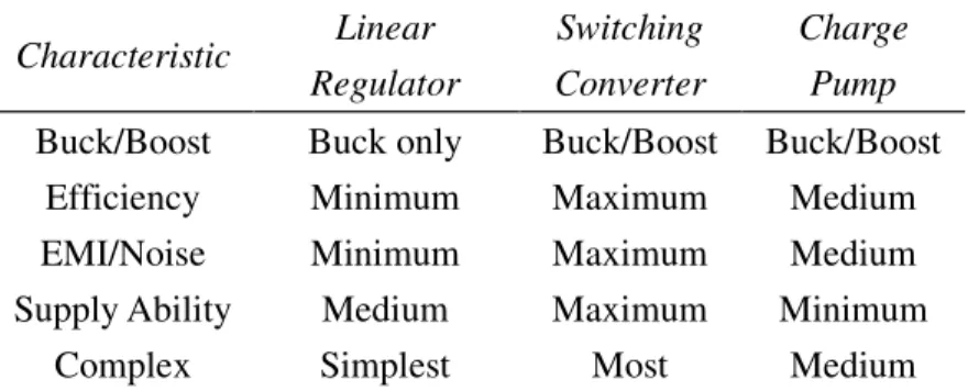
TABLE I COMPARISONS OF DIFFERENT TYPE REGULATORS. ... 6
TABLE II COMPARISONS OF DIFFERENT TYPE PASS DEVICES. ... 20
TABLE III SPECIFICATION OF CFCLDOREGULATOR. ... 58
TABLE IV PARAMETERS OF LDO UNDER LOAD CURRENT 50µA. ... 61
TABLE V ACPARAMETERS OF CFCCAPACITOR-FREE LDO UNDER LOAD 50µA. ... 61
TABLE VI ACPARAMETERS OF CFCCAPACITOR-FREE LDO UNDER DIFFERENT LOAD. ... 62
TABLE VII POLES AND ZERO LOCATIONS WITH OFF-CHIP CAPACITOR 10µF AND ESR1Ω. ... 65
TABLE VIII LOAD TRANSIENT COMPARISONS W/O AND W/I CFCTECHNIQUE. ... 73
TABLE IX PERFORMANCES OF CFCLDOREGULATOR... 75
TABLE X MEASUREMENT RESULTS OF CFCCAPACITOR-FREE LDOREGULATOR. ... 81
Chapter 1
Introduction
Power management has become a more and more popular topic in recent years, especially for the battery-operated portable devices due to the longer using time. In other words, using the energy economically and power-saving techniques due to efficiency enhancement are two major solutions to achieve this target. In this chapter, we will show you why we need power management systems and what it is in Chapter 1.1 first. Second, we give a brief introduction about power management system common blocks, such as switching converters, liner regulators, and charge pump converters, and compare these different regulators in Chapter 1.2. In Chapter 1.3, we will show you why the linear regulators are the most common and important block in power management system. Finally, we will give our motivation in Chapter 1.4.
1.1 Power Management system
With the explosion development of integrated circuit, more and more functions are embedded in a device to meet the consumer requirement. As shown in Fig. 1, the growing of battery energy is not satisfied to chip requirement. But the running time of the portable devices, such as the lap tap, mobile phones and digital cameras, is a very important requirement for the consumers. Therefore, how to save the battery energy and use it more efficiently is the most important topic.
As mentioned before, the increase of battery content doesn’t satisfy device requirement. In the other way, we must construct a power system using energy as economically as possible. As shown in Fig. 2, it may have many powered devices for a portable device. For example, a mobile phone may need at least five regulated voltages, one buck converter for core CPU, one boost converter for cooler LCD panel, one high PSRR LDO regulator for RF power amplifier, one LDO regulator for analog base-band, and one charge pump for white light LED driver. These blocks are only needed powered when the function are active. Therefore, the control unit of power management system has ability to shutdown, sleep, or active some power sources depended on the powered devices requirements. On the other hand, we can also enhance the efficiency of power sources, such as switching converter, linear regulator, and charge pumps. In this way, we can decrease the power dissipation to the minimum, and enhance the operating time to the longest. This is why the power management system becomes more and more important, especially for portable devices.
1.2 Introduction to Different Regulators
In this section, we will give a brief introduction to three types of most common regulators, linear regulator, switching converter, and charge pump. Finally, we give a comparison about these three types of regulators.
1.2.1 Linear Regulator
As shown in Fig. 3, the linear regulator consist of a error amplifier to correct input and output difference, a pass device to supply load current, and a resistive feedback network. The structure is the most compact without complex control circuit, results in smaller chip size and cost. The linear regulator utilizes the feedback network to construct shut negative feedback effect to regulate the output voltage. In this way, this kind of regulator does not need switching clock, so the output noise can be minimized and the output voltage does not exist ripple. Without dual storage components, linear regulator only can be operated in buck operation. The efficiency of linear regulator is about the output voltage dividing input voltage. The highest
efficiency occurs that output voltage is near input voltage, i.e. low dropout operation. The supply load ability depends on pass device’s size.
1.2.2 Switching Converter
As shown in Fig. 4, this is a conventional voltage mode switching buck converter. It compares the output voltage with reference voltage to decide the duty cycle. When power PMOS conducts, the supply voltage will charge the inductor and capacitor. And in the next time, the power NMOS conducts, so the inductor will be discharged to the capacitor. Due to dual storage components, inductor and capacitor, the switching converter can be operated in buck or boost operation. Generally speaking, the efficiency can be achieved above 90% under heavy load condition. Meanwhile, with higher switching frequency in the range of hundreds of Kilo-Hertz to several Mega-Hertz, the storage components can be designed smaller to save the cost. But the EMI and noise problems become critical. Depended on efficiency requirement, the control circuit is much larger than the other two and the cost is the most. The supply
load ability is the largest always in the range about hundreds of milliamps to several amps.
1.2.3 Charge Pump
As shown in Fig. 5, this is a conventional charge pump converter. During ψψψψ1111
phase, the input voltage charges Cs to input voltage. During ψψψψ2222 phase, the output
equals to input voltage adding voltage across Cs, and gets twice input voltage. With
hysteric feedback control, the output is regulated at desired output voltage. The charge pump can also be operated in buck or boost mode, but the efficiency is higher in boost mode. The control circuit is more compact than switching converters, but more complex than linear regulators. Due to switching clock, charge pump also suffers from EMI and noise problems. But these problems are slighter than switching converters’, results from smaller switching frequency in the range of hundreds of Kilo-Hertz. The supply load ability of charge pump is weak, because this depends on capacitor size and switching frequency.
Load Vin Gate Driver Vout VREF CMP Ramp Generator L C Mp Mn Error Amp
1.2.4 Comparison
In the above discussion, each type of regulator has its own advantages and disadvantages. Before deciding using which type of regulators as power source, you must take a good tradeoff between these characteristics.
TABLE I
COMPARISONS OF DIFFERENT TYPE REGULATORS.
Characteristic Linear Regulator Switching Converter Charge Pump
Buck/Boost Buck only Buck/Boost Buck/Boost
Efficiency Minimum Maximum Medium
EMI/Noise Minimum Maximum Medium
Supply Ability Medium Maximum Minimum
Complex Simplest Most Medium
1.3 Importance of Linear Regulator
The linear regulator is wildly used in power management system due to the compact structure results in low cost advantage. Meanwhile, without switching
topology, the EMI and noise issues are minimized, especially for audio devices. On the other hand, the linear regulator can be cascaded before a charge pump as shown in Fig. 6. The linear regulator can supply a pre-regulated output voltage for charge pump, which input ripple and noise are minimized. This topology is widely used in white LED driver.
Meanwhile, the linear regulator can be cascaded after a switching converter or charge pump as shown in Fig. 7. The linear regulator is served as a post-regulator in order to minimize the output noise and ripple required by powered devices.
Via the above discussion, we know that linear regulators are the key and most common component in power management system. For modern power management system, designing a high performance linear regulator is essential. But there are still many difficulties in designing a high performance linear regulator.
Fig. 6. Linear regulator served as pre-regulator.
1.4 Motivation
As well known, conventional low-dropout liner regulator is compensated by the equivalent series resistor (ESR). However, this kind compensation is hardly to maintain because gain and poles locations are varied with load conditions. In the recent years, the demanding for high performance liner regulator such as high resolution and high power supply rejection is getting growing. The Multi-stage LDO can achieve this target. Meanwhile, with the development of SoC system, a capacitor-free LDO is preferred to reduce the board space and cost greatly. However, the most important disadvantage of Multi-stage LDO is the limitation of minimum load.
Therefore, a current feedback compensation (CFC) technique for capacitor-free LDO regulators with adaptively adjusting the phase margin is proposed in this thesis. CFC technique can adaptively adjust the phase margin for achieving better transient response than that with variant phase margin at different load current conditions. Not only fast transient response is attained due to suitable phase margin but also the minimum load current limitation can be greatly reduced to about 50µA without sacrificing bandwidth at light load current condition. Besides, CFC technique can have high PSRR bandwidth with compatible compensation capacitors compared to the Q-reduction technique. The capacitor-free LDO regulator with CFC technique is fabricated by TSMC 0.35µm 2P4M CMOS process with small compensation capacitors 5pF and 1.5pF. Experimental results demonstrate that the minimum load can be reduced to 50µA and transient response time with adaptively phase margin control is smaller than 1µs.
Chapter 2
Convention al and Proposed LDO
Regulators
From the previous discussion, the linear regulator is the most common component of power management system. With requirement of high performance LDO regulator, such as high load and line regulation, high power supply rejection ability, and fast transient response, the LDO regulator design becomes more and more difficult. In this Chapter, we will give you a complete introduction of low dropout voltage (LDO) regulator, and point out what problems they have. In the Chapter 2.1, we will give you an overall introduction to linear regulator performance definition first. Second, we will describe how a conventional LDO regulator works and what problems it has in the Chapter 2.2. Third, in order to solve the conventional structure problems, many structures have been proposed. But they inherently have lots of problems, we will show then in Chapter 2.3. Finally, to enhance LDO regulator performance dramatically, multi-stage LDO regulator design has been proposed. Inevitably, this kind of topology has many unsolved problems. Therefore, we will describe it in the Chapter 2.4.
2.1 Definitions of LDO Regulator
In this section, we will show you the LDO regulator’s performance definitions, such as dropout voltage, quiescent current, efficiency, transient response, line and load regulation,
power supply rejection, and accuracy [1][2].
2.1.1 Dropout Voltage
The dropout voltage means that the difference between input voltage and output voltage when the shut feedback effect ceases to regulate the output voltage to a desired value under the maximum load condition. To more specified definition, the dropout voltage occurs at the output voltage drifted 2% of its value. When the dropout region occurs, the pass device is operated in linear region. Therefore, the dropout voltage can be expressed in equation (1).
dropout o on
V
=
I R
(1)In modern LDO regulator design, efficiency is the most concerned performance. The dropout voltage is always designed about 200mV under maximum load current condition. In order to achieve low dropout voltage maintaining high efficiency, one way is to increase the power MOS size, but this will increase the chip size and results in more complex compensation. The other way is to increase the loop gain. The larger loop gain can maintain the regulation even if the power MOS operated in linear region.
Ooutp ut Volta g e Input Voltage Regulation Region Dropout Region Off Region Vin Vout Dropout Voltage
2.1.2 Efficiency
The efficiency of linear regulator is defined as output power divide input power. The output power equals to output voltage multiply load current. The input power equals to input voltage multiply with load current and quiescent current. The quiescent current consists of bias current such as error amplifier bias current, band-gap reference current, feedback resistance network, and so on. In heavy load, the load current is far larger than the quiescent current, and the efficiency depends on the difference between input and output voltage, i.e. dropout voltage. In light load, the quiescent current may be near the load current, and the efficiency is further decreased. Therefore, we must minimized quiescent current at light load condition and the dropout voltage to achieve higher efficiency performance.
100%
(
)
Load o Load q iI
V
Efficiency
I
I V
=
×
+
(2)100%
(
)
Load current Load qI
Efficiency
I
I
=
×
+
(3)2.1.3 Transient Response
Transient response is the dynamic performance of linear regulator [3]. It can be separated into two parts, one is form load variation, named as load transient response, and the other is from line variation, named as line transient response.
As shown in Fig. 9, when the linear regulator suffers a load step current variation, the output voltage will be existed in a transition and variation period. During a load-transition from light load to heavy load, the pass device can’t supply such large load current instantly. Therefore, the output voltage experiences a voltage drop. The drop period Δt1 depends on
Fig. 9. Load transient response. time can be approximate in the following equation:
1
1
1
sr par cl cl srV
t
t
C
BW
BW
I
∆
∆ ≈
+
=
+
(4)where BWcl is the close-loop bandwidth of the linear regulator, Cpar is the parasitic capacitor
of the power MOS at gate terminal, Isr is the bias current under slewing condition.
Due to this response time, the power MOS can’t support load current requirement. The load will discharge the output capacitor and cause a voltage drop at this moment as shown in the Fig. 10.
Fig. 11. Output drops during heavy to light load.
The output voltage drop depends on the output slew rate limitation Io,max/COUT and the
system response time ΔVtr,max. The frequency compensation resistor RESR but also
contributes an ESR drop ΔVESRduring transient. The equation is shown in the following:
,max ,max 1 o tr ESR OUT
I
V
t
V
C
∆
=
∆ + ∆
(5)Finally, the system will enter in small signal settling region. During this period, the system response is relative to the closed loop bandwidth and phase margin.
For the same reason, during a load-transition from heavy load to light load, the pass device can’t shut the power MOS quickly. Therefore, the output voltage experiences a voltage peak. The response is the same as mentioned before, but the voltage peak response has some differences with voltage drop due to resistor RESR. Since the load step sharply, the power MOS
can’t shut rapidly. The redundant current will charge the output capacitor with additional ESR peak as shown in Fig. 11.
In the next time, the power MOS has been shunt off, and the unnecessary charge on the output capacitor will be discharge through the resistive network causing a voltage drop as show in Fig. 12. Finally, the output will settle to the desired voltage.
Fig. 12. Output discharge through resistive network.
means that the output variation under input voltage step. The line transient response is like load transient response. When the input step to a smaller value, power MOS will support less load current casing output drop. The response is like load current with light load to heavy load. When the input step to a larger value, power MOS will support more load current casing output peak. The response is like load transient with heavy load to light load.
For the above discussion, to obtain better transient response, a higher bandwidth of linear regulator, faster slewing at power MOS gate terminal, larger output capacitor, and smaller ESR are recommended.
2.1.4 Line & Load Regulation
Line and load regulation are steady-state performances of linear regulator. These performances are two important specifications that related to output voltage accuracy. The line regulation means that the output voltage variation at different input conditions as shown in Fig. 14. To get better line regulation, a higher loop gain is required, but the stability is sacrificed. There is a tradeoff between precision and stability.
1
(
)
OUT m o REF IN o INV
g r
V
Line Regulation
V
L
β
V
∆
∆
=
≈
+
⋅
∆
∆
(6)where Lo is the loop gain of linear regulator, gm and ro are the transconductance and output
resistance of power MOS, β is the feedback factor.
Fig. 15. Definition of load regulation.
The load regulation means that the precision of output voltage under different load conditions as shown in Fig. 15. In order to get better load regulation, a higher loop gain is still required, but the stability problem must be concerned.
1
OUT o OUT oV
r
Load Regulation
I
L
∆
=
= −
∆
+
(7)where Lo is the loop gain of linear regulator, ro is the output resistance of power MOS.
2.1.5 Power Supply Rejection (PSR)
Power supply rejection is a highly important performance of linear regulator. Since it does not using switching type to regulate output, it is widely cascaded before or after the switch type converter to be served as pre-regulator or post-regulator in order to minimize the input supply noise, especially for audio applications [4]-[6].
Due to the shut feedback of linear regulator, the output resistance is reduced a factor of loop gain, Lo. Zo is the open loop output resistance to the ground, which shown in equation (8).
Fig. 16. Approximate modeling of PSR.
condition, which is given is equation (9).
1 2
(
) || (
)
o OUT ESRZ
=
Z
+
R
R
+
R
(8)||
o o o shunt oZ
r
Z
L
−=
(9)Therefore, the PSR performance of linear regulator can be approximate as simply voltage divider as shown in Fig. 16, which given in equation (10).
(
||
)
(
||
)
OUT o o shunt DD o o o shuntV
Z
Z
PSR
V
r
Z
Z
− −=
=
+
(10)At lower frequency, the shunt feedback is largest due to highest loop gain, so Zo-shunt is
the dominant term. And PSRdc can be approximate by voltage divider as following:
1 2 1 2
|| (
)
1
|| (
)
o o shunt o dc o o o shunt o o or
R
R
R
L
PSR
r
R
R
r
R
L
r
L
− −+
≈
=
≈
+
+
+
(11)As the frequency increased, the loop gain will be initially to decay at the bandwidth,
BWA, of the error amplifier, i.e. the shut feedback is deteriorated. This will cause a PSR zero
-1 ol
(A β)
Fig. 17. PSR frequency response.
output resistance, since the loop gain has decayed under 0 dB. The PSR can be approximate as following: 1 2 1 2
(
)
1
(
)
o UGF o o oZ
R
R
PSR
r
Z
r
R
R
+
≈
=
≈
+
+
+
(12)At higher frequency, the output capacitor begins to shut the (R1+R2) to the ground. The
PSR will be improved at output pole. Finally, if the system has ESR, the ESR will cause a PSR zero at high frequency as shown in equation (13).
o ESR f UGF o o o ESR
Z
R
PSR
r
Z
r
R
>>≈
=
+
+
(13)The PSR frequency response can be approximate in Fig. 17. The DC value of PSR is about the reciprocal of loop gain, Lo. With frequency increased to bandwidth of loop gain, the
PSR will be deteriorated. The PSR will be decayed to 1 at unit gain frequency of loop gain. Finally, the output will shunt the resistive feedback network to the ground and improve the PSR performance.
2.1.6 Accuracy
The accuracy of linear regulator is considered all the effects, line regulation (∆VLR), load
regulation (∆VLDR), reference voltage drift (∆Vo,ref), error amplifier drift (∆Vo,a), feedback
resistor tolerance (∆Vo,r), and temperature coefficient (∆VTC), contributing to output voltage
variation. The accuracy equation can be described in the equation (14).
2 2 2 2 , , ,
|
|
|
|
100%
LR LDR o ref o a o r TC oV
V
V
V
V
V
Accuracy
V
∆
+ ∆
+ ∆
+ ∆
+ ∆
+ ∆
≈
×
(14)The typical implementations achieve roughly 1% to 3% overall accuracy, results from all the disturbances described before.
2.2 Conventional LDO Regulators
There are many different types of pass device topology, such as NPN-Darlington type, bipolar types, and MOS types. We will show you what type is preferred with different applications. And then we will give a small signal analysis about low-dropout voltage linear regulator.
2.2.1 Types of Pass Device
The bipolar types of pass device shown in Fig. 18, NPN-Darlington, NPN, PNP can deliver the highest load current to output, which need larger biasing current. Due to biasing current, bipolar types of pass device are usually in high-speed operation. For the efficiency-concerned deign, low quiescent current and low dropout voltage are preferred. For low quiescent current purpose, MOS types are better than bipolar ones. For low dropout voltage, PMOS and PNP types are preferred, but PNP type needs large quiescent current due to smaller current gain. For the efficiency-priority LDO regulator, MOS types pass device are usually adopted. For PMOS type, the dropout voltage is the minimum, but the frequency
Fig. 18. Types of pass device.
response is more difficult results from large gate-to-drain capacitor Cgd with Miller effect. For
NMOS type pass device, the most advantageous due to its low on resistance results in easier compensation and better PSR performance. If the NMOS type must be operated in low dropout, the charge pump is needed, which increases the circuit complexity. Generally speaking, we usually use PMOS type pass device to achieve LDO regulator design [7][8].
TABLE II
COMPARISONS OF DIFFERENT TYPE PASS DEVICES.
Darlington NPN PNP NMOS PMOS
Iout High High High Medium Medium
Iq Medium Medium Large Low Low
Vdropout Vce(sat) +2Vbe Vce(sat) +Vbe Vce(sat) Vgs+Vds(sat) Vds(sat)
Speed Fast Fast Slow Medium Medium
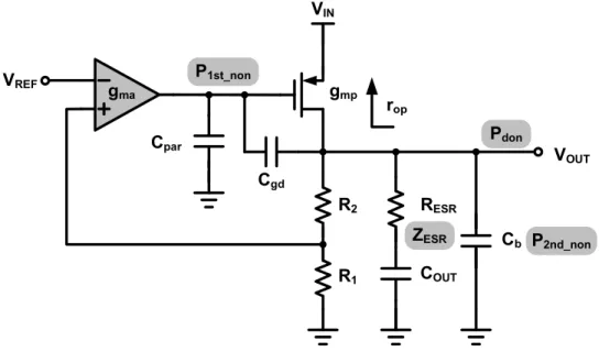
2.2.2 Conventional LDO Regulators
As shown in Fig. 19, the conventional LDO regulator consists of a error amplifier with one dominant pole located at its output, one power PMOS pass device with gate capacitance
Cpar, and large gate-to-drain capacitor Cgd, a resistive feedback network R1 and R2, an output
capacitor COUT with an equivalent serial resistor RESR for compensation, and a bypass
capacitor Cb to reduce high frequency noise and help transient response [9]-[13].
Due to huge output capacitor with large output resistance of power PMOS and large gate capacitance Cpar associated with huge output resistance of error amplifier Roa to
achieve high gain, the system has two low frequency poles. This system needs to be compensated. The most common compensation technique is adding an equivalent resistor to create a low frequency zero to compensate the first non-dominant pole located at power MOS gate terminal. There still exists in a higher frequency pole which associated with bypass capacitor and ESR. The overall poles and zero is shown in equation (15)-(18):
VREF gmp R2 R1 RESR COUT Cb VOUT Cpar Cgd gma Pdon P1st_non ZESR P2nd_non VIN rop
1
don op OUTP
r C
=
(15) 1 _1
st non oa parP
R C
=
(16) 2 _1
nd non ESR bP
R
C
=
(17)1
ESR ESR OUTZ
R
C
=
(18)The ESR compensation technique exists in a stability problem resulting from non-constant unit gain frequency. As load increased, the dominant pole will move to higher frequency which is proportion to load current Ilaod as shown in equation (19). Meanwhile, the
loop gain will be decayed which is inverse proportion to radical of load current Ilaod as shown
in equation (20).
1
1
1
don load op OUT loadP
I
r C
I
λ
=
∝
=
(19)1
1
o oa p oa mp op load load loadL
A A
A g r
I
I
I
β
β
λ
=
=
∝
×
=
(20)where rop is the output resistance of power PMOS, COUT is output capacitor, is λ is the
channel length modulation parameter, Lo is the open-loop gain, β is the feedback factor,
Aoa is error amplifier gain, Ap is power PMOS gain, gmp is transconductance of power PMOS.
As shown in Fig. 20, if the ESR zero was chosen to compensate the first non-dominant pole, it must be located before the magnitude decayed under 0 dB. As load current increased, the dominant pole moves to high frequency faster with loop gain decayed not in the same speed, the system may be unstable, which results from the magnitude is not decayed under 0 dB before second non-dominant occurs. With the same reason, if we compensate in heavy
Fig. 20. Difficulty of ESR compensation.
load. The system still may be unstable in light load condition. Therefore, there is no simple rule to define ESR compensation due to variable unit gain frequency. Meanwhile, the compensation ESR will cause additional voltage drop under transient response.
2.3 Proposed LDO Regulators
Since the ESR compensation is hard to assure the stability under different load conditions and exists in unwilling voltage drop, there are many topologies have been proposed. In this section, we will show you some resolutions to ESR compensation technique.
2.3.1 Miller Compensation
In order to keep the unit gain frequency constant, Miller compensation technique is the intuitive method as show in Fig. 21. Utilizing the power PMOS gain, the Miller effect of
compensation capacitor Cm will cause a dominant pole located at power PMOS gate terminal
as shown in equation (21). The first non-dominant located at output can be approximate with
Cm short as shown in equation (22). Due to large output capacitor, the
Fig. 21. Miller compensation technique for LDO regulators.
chip area. The Miller compensation capacitor connected across the power PMOS gate-to-drain will cause power supply noise directly couples to the output, and the power supply rejection will be sacrificed greatly. This kind compensation is not a good choice [14][15].
1
don mp op m oaP
g R C R
=
(21) 1 _ mp st non OUTg
P
C
=
(22)where gmp is transconductance of power PMOS, Rop is the output resistance of power PMOS,
Cm is compensation capacitor, COUT is output capacitor, Roa is the output resistance of error
amplifier.
2.3.2 Insert a Buffer Stage
The dominant pole compensation mentioned before has several drawback, such as bandwidth reduction, large compensation capacitor, and poor PSR performance. The buffer
Fig. 22. Buffer stage for LDO regulator.
stage for linear regulator has been proposed. The buffer stage has characteristics of low input capacitor and low output resistance, splitting the pole at power MOS gate to two high frequency poles [16]. The overall system will be approximate a dominant pole system located at output. And the buffer stage can be a current-efficient stage which helps to enhance slewing ability at power PMOS gate. But the drawback is that the buffer stage is always formed a PMOS or NMOS common-drain stage, i.e. a level shifter, there will be at least a Vt drop to
drive power MOS. Therefore, with a PMOS CD stage, the power PMOS can be fully turned on, results in a large power MOS is needed. On the other hand, with a NMOS CD stage, the power PMOS can be fully turned off, the quiescent current may be large. This is the main disadvantages of buffer stage for LDO regulator.
2.4 Multi-Stage LDO Regulators
The ESR compensation suffers from difficult compensation problem and ESR voltage drop. The dominant pole compensation sacrificed the bandwidth considerably with large compensation capacitor. The buffer stage confronts fully turn on and off problem, results in larger power MOS size or quiescent current. In recent days, the multi-stage LDO regulator
has been proposed to achieve high performance [17]-[23]. Due to multi-stage structure, the loop gain may be over one hundred decibel, causing the performance further improved such as line and load regulation, power supply rejection. Furthermore, the most attractive advantage of this kind LDO regulator is that it can be operated at capacitor-free condition with faster response resulting from a wider bandwidth. This reduced the PCB area greatly, especially for system on chip (SOC) application. But the multi-stage LDO regulator design has several unresolved problems. We will show you in this section.
2.4.1 Three-Stage LDO with Pole-Splitting
Compensation
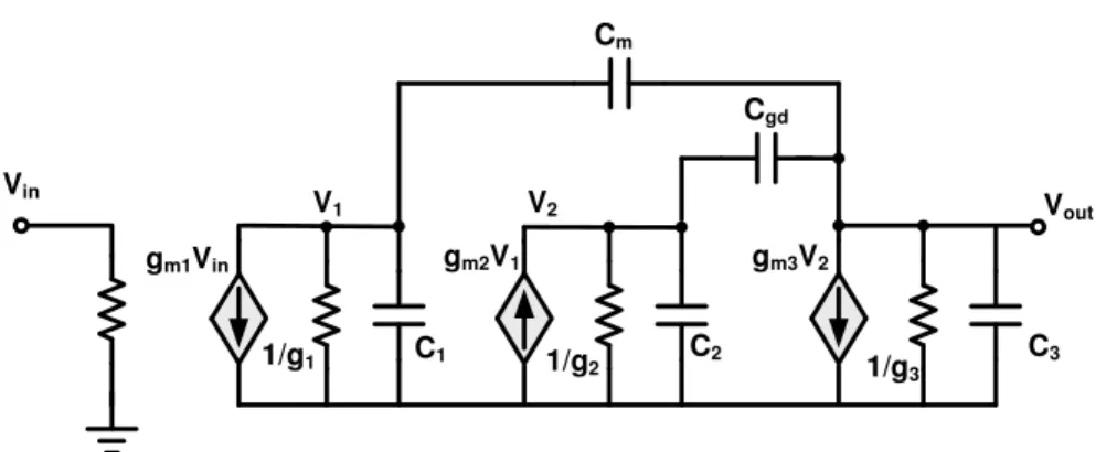
The multi-stage LDO regulator usually consists of three-stage, one is the first high gain stage gm1, gmcf, and a second gain stage gm2, and the power PMOS acting as third gain stage.
The system at least has three poles, output of first stage, output of second stage, and output
stage which C3 modeling the parasitic capacitor of power PMOS. Under capacitor-free
Fig. 24. Single Miller capacitor compensation for three-stage LDO regulator.
condition, the feedforward stage gmf forms the push-pull stage to help the slewing at power
MOS gate. And this stage will be adding a zero to help the system stability. There are many compensation techniques for three-stage amplifier design, such as nested Miller compensation, damping-factor-control compensation, and transconductance feedback compensation. But in LDO regulator design, due to large power PMOS associated with large gate-to-drain capacitor
Cgd, about 7 pF in this paper, the various types of compensation technique may not be suited
for LDO regulator design.
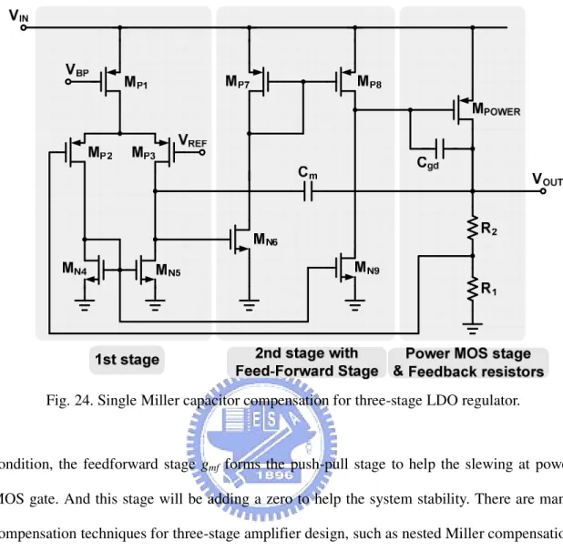
As shown in Fig. 23, this is the simplest three-stage LDO regulator with dominant compensation capacitor Cm. Associated with large gate-to-drain capacitor Cgd, this system is
inherently a nested Miller compensation (NMC) structure [24][25].
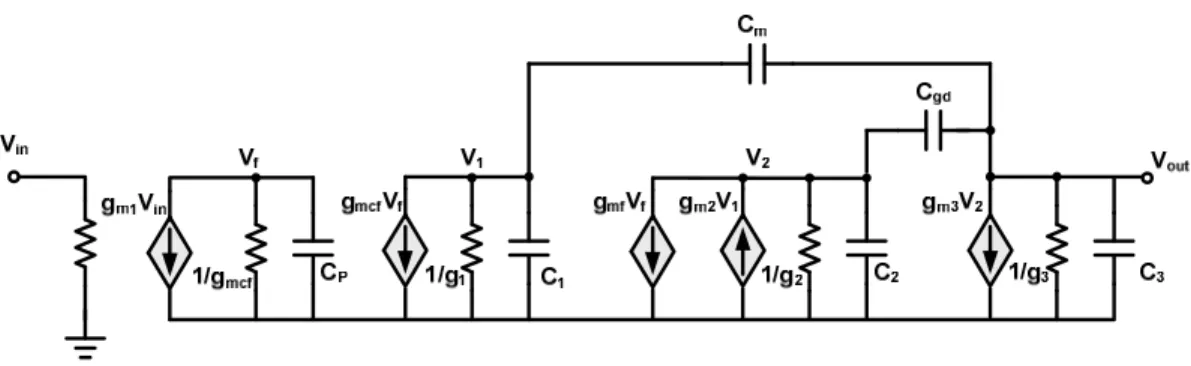
The circuit level of SMC LDO regulator is shown in Fig. 24. The first stage consists of transistors MP1~MN5. Transistors MN6~MP8 forms the second stage. Transistor MN9 is the
response. The power MOS stage acts the third stage.
The analysis structure can be used Fig. 25. The gm1 is the transconductance of input
differential pairs MP2 and MP3, gmcf is the transconductance of current mirror load MN5, gm2 is
the transconductance of MP8, gmf is the transconductance of MN9, and gm3 is the
transconductance of MPOWER. The g1-2 and gp are the output reactance of each stage and the Cp,
C1-2, and C3 are the lumped parasitic capacitor of each stage. The huge gate-to-drain capacitor
is represented as Cgd. The capacitor Cm is the compensation capacitor.
The small signal analysis is shown in Fig. 26. Using KVL and KCL theorems, the transfer function from input to output can be expressed in equation (23):
2 2 2 3 2 1 2 3 3 2 2 2 3 1 2 3 1 2 3 2 3 3 2 2 3 2 2 2 3 2 2 3 3 2 2 3 2 3 2 3
1
(
)
(1
)[
1]
1
(
)
(
)
(1
)[
1]
m mf m m m mcf m out m m m m m m gd in m m m m m m m m m mf m m m mcf m o gd m gd m m dB m m m m mC g
C C
s
s
g g
g
g
V
g g
g
g
g
C C
C C
s
V
g g g
s
s
g g g
g
g
g g C
C g
g
C g
C C
s
s
g g
g
g
A
C
C C
C C
g
g
s
s
s
p
−g
g
g g C
−
−
= −
−
+
+
+
−
−
= −
+
−
+
+
+
(23)where Ao is the DC loop gain, P-3dB is the dominant pole of this system.
The system exists in three poles and one zero system can be shown in equation (24)- (27): 1 2 3 3 2 3 dB m m m
g g g
p
g
g C
−=
(24) 1 mcf mg
z
C
=
(25) 3 2 1 2 2 3,
m gd,
m st non nd non gdg C
g
p
p
heavy load condition
C
C C
−=
−=
(26) 2 3 2 3 2 3 2 3 2 3 3 2,
,
(
)
m m m m m o m m m m m gdg
g
C C
g
g C
Q
light load condition
C C
g
g
g
g
C C
ω
=
=
−
(27)At heavy load, the system has one dominant pole, two separate non-dominant poles, and one zero. This zero is to compensate the first non-dominant pole under the heaviest load. As the load decreases, the first non-dominant will move to higher frequency slightly, and the second non-dominant pole will move to lower frequency, results the complex poles generation. When the load further decreases, the natural frequency will also decrease with the damping factor Q increased, which deteriorates the stability seriously. At ultra light load, the complex poles even move to right-half-plane, results in light load oscillation. The pole-zero location is show in Fig. 27.
Fig. 27. Pole-zero location of SMC LDO regulator.
Just like nested Miller compensation, the single Miller compensation LDO regulator with embedded large gate-to-drain capacitor Cgd is a NMC structure inherently. Therefore, as the
mentioned nested Miller compensation, the output transconductance gm3 must be much larger
than the second stage’s gm2, which causes large power consumption. Meanwhile, for the
capacitor application, the transconductance of second stage gm2 must be set large to improve
transient response. Therefore, the minimum load current, i.e. current in the feedback resistor, must be large in the order of several mini-amps, causing low light load efficiency.
m M
G (transconductance of input stage) UGF = C (CompensationCapacitor) G a in -d B
2.4.2 Three-stage LDO with Damping-Factor-Control
Compensation
There are many compensation techniques for three-stage amplifier design [26]-[30] which have been proposed, such as active feedback compensation (AFFC), damping factor control compensation (DFC), transconductance feedback compensation (TCFC), and so on. The damping factor control is the first implement for multi-stage LDO design proposed in [17]. The damping factor block will cause a low resistance at high frequency, results in higher natural frequency and lower damping factor. The DFC block design proposed in [17], the compensation capacitor Cm2 must be set equal to Cm1 and the transconductance of damping
factor stage gmd must be set four times of input transconductance gm1 to ensure stability, which
cause large chip size and larger power consumption. The minimum load current is about 100 µA to 10 mA depending on design. This restriction comes from that the design [17] does not
concerned the large gato-to-drain capacitor Cgd of power PMOSFET carefully.
2.4.3 Three-stage LDO with Q-Reduction
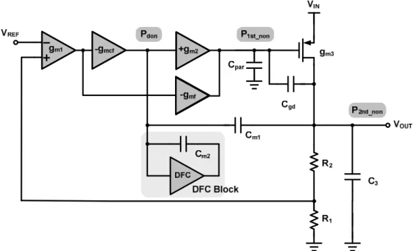
Compensation
Although there are many compensation techniques for three-stage amplifier designs, there is no one suited for LDO regulator design, due to the NMC structure inherently. Therefore, the Q-reduction technique has been proposed in [18].
The circuit level of Q-reduction compensation LDO regulator is shown in Fig 31. The first stage consists of transistors MP1~MN5. Transistors MN6~MP8 forms the second stage.
Transistor MN9 is the feed-forward stage which forms push-pull stage associate with transistor
MP8 to help transient response. The power MOS stage acts the third stage. The proposed
Q-reduction compensation capacitor Ccf is connected from the gmcf stage to the output of the
second stage.
After small signal analysis, the input to output transfer function at light load can be expressed in equation (28). The natural frequency ωo is slightly reduced by Ccf shown in
equation (29) and the damping factor shown in equation (30) is reduce by the terms,
CcfC3gm2+CmCcfgm2gm3/gmcf, compared to equation (27). 2 2 1 2 3 2 3 3 3 2 2 3 2 3 2 2 3 2 3 1 2 3 2 3 2 3 2 2 1 2 3 2 1 ( ) [ ] ( ) (1 ) [1 ] 1 ( ) [ mf m gd m cf gd cf cf cf out m m m m m m o m m m gd m cf m m cf m cf m m m in m m m m m mf m gd m cf cf m m m m m o g C C C C R C C s C R s V g g g g g g A g g C C g C C g g R C C g g C C C V s s s g g g g g C g g g C C C C s C R s g g g g g A + + − − + = − − + + + ⋅ + + + + − − = − 3 3 3 2 2 3 2 3 2 2 3 3 2 3 2 3 ] ( ) (1 ) [1 ] cf gd cf m m m m gd m cf m m cf m cf dB m m m m m R C C g g g C C g C C g g R C C C C s s s p− g g C g g + − + + + ⋅ + + (28) 2 3 2 3 m m o
g
g
C C
ω
=
(29) 2 3 2 3 2 3 3 2 2 3 2 31
(
)
m m m m m m m m gd m cf m m m cf mcfC C
g
g C
Q
g
g
g
g
C C
g C C
g
g C C
g
=
−
+
+
(30)Fig. 32. PSR performance of Q-reduction compensation.
The most important drawback of Q-Reduction compensation is that the compensation capacitor connected form the power MOS gate to the ground reference, degenerates the auto-cancellation at the gate and source of power PMOS. This will result in the mid-frequency PSR deterioration as shown in Fig. 32.
2.4.4 Equivalent Two-Stage LDO Design
Unlike conventional dominant compensation of LDO regulator, the equivalent two-stage LDO regulator has been proposed in [31]. This structure consists of two stage MP6~MP10 with
high frequency poles, so the system can be approximate as a two poles system located at output of first stage and output as shown in equation (31)(32). The compensation capacitor Cm
can be connected from ground reference to the output instead, and the power supply rejection performance will not be degenerated.
3 1 2
1
dB o m op mp
R g
R C
−=
′′
(31) 2 1 m st non Lg
p
C
−′′
=
(32)Fig. 33. Equivalent two-stage LDO regulator.
where Ro1, Rop are the output resistance of first and output stage, gm2” is the equivalent
transconductance of second stage, Cm, CL are the compensation and load capacitor.
The above assumption is held under the second non-dominant pole at power MOS gate will not affect the system. This structure utilize resistive load RB1 to cause higher frequency
second non-dominant, and the PSR performance is improved. When the load increases, the output pole will move to higher frequency. The switch MP11 will be turned on, the second
non-dominant pole will also move to higher frequency preventing from complex poles generation to ensure the system stability. At the same time, the power MOS stage using cascade topology, MPOWER1and MPOWER2, minimize the Miller effect of gate-to-drain capacitor
Cgd of MPOWER1, i.e. the gain of power MOS MPOWER1 equals to one. This topology will
Chapter 3
Current Feedback Compensation for
Capacitor-Free LDO Regulators
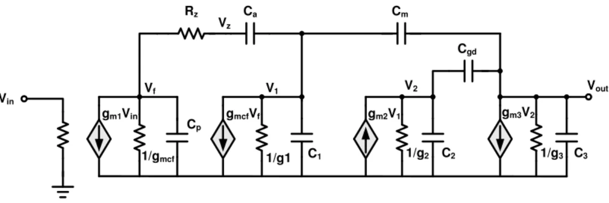
From the discussion in Chapter 2, the ESR compensation is hardly to ensure the stability under different load condition, which results from non-constant unit gain frequency. And the ESR will cause unwilling voltage dip during transient period. Then the compensation techniques without ESR are developed, such as Miller compensation and inserting a buffer stage. The Miller compensation technique needs large compensation capacitor and the bandwidth is reduced greatly. The buffer stage compensation has fully turned on and off problems. For now days, the high performance LDO regulator has be proposed, i.e. high load regulation and high power supply rejection. The multi-stage LDO design can achieve this target. But the three-stage LDO regulator with Miller compensation inherently forms a nested Miller compensation topology, causes a minimum load restriction. Therefore, the DFC compensation method proposed in [17]. But the NMC embedded structure degenerates the DFC block effects. And the Q-reduction method has been proposed in [18], the minimum load can be down to 100 µA. But this kind compensation deteriorates the PSR performance seriously. In this Chapter, we will propose a new frequency compensation technique, current feedback compensation for three-stage LDO regulator, which can be operated in ultra light load operation and with high power supply rejection and faster transient response.
3.1 Three-Stage LDO Regulator with Resistive
Load at Second Stage
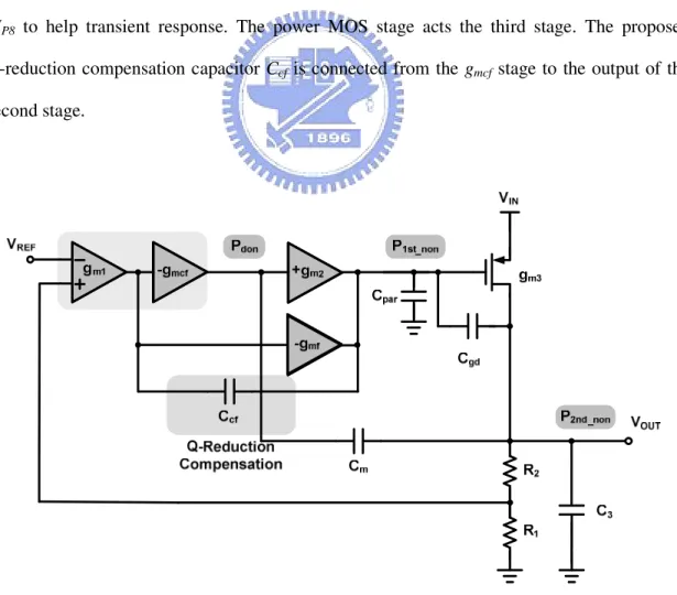
In the chapter 2.4.4, the equivalent two-stage LDO has been proposed. If there is no cascode power PMOS topology under capacitor-free condition, the system will be consist of one dominant pole and a pair of complex poles. The generation of complex poles will result in the minimum load restriction, but the smaller output resistance of the second stage by using resistive load will alleviate this effect and increase the power supply rejection performance by the same fluctuation at power PMOS gate and drain terminal.
The circuit level of three-stage LDO is shown in Fig. 34. The first stage consists of transistors MP1~MN5. The second stage consists of transistors MN6~MP10 with resistive load RB.
The power PMOS stage acts the third stage.
The analysis structure can be used Fig. 35. The gm1 is the transconductance of input
differential pairs MP2 and MP3, gm2 is the equivalent transconductance of MP8 ~MP10, and gm3
is the transconductance of MPOWER. The g1, g2, g3 are the output reactance of each stage and the
C1-3 are the lumped parasitic capacitor of each stage. The huge gate-to-drain capacitor is
represented as Cgd. The capacitor Cm is the compensation capacitor.
Using KVL and KCL theorems, the transfer function from input to output can be expressed in equation (33): 2 2 1 2 3 2 3 3 2 3 3 2 3 2 3 2 2 3 1 2 3 1 2 3 1 2 3 1 2 3 2 2 2 3 3 2 3 3 2 2 2 3 3 2 3 2 3
1
(
)
1
1
(
)
(1
)[
1]
gd m out m m m m m m m m m m gd m m m m in gd m m m m o m m m m gd db m m m m mC
C C
s
s
V
g g
g
g
g
g
g C C
g
g
C C
C C C
g
g C
V
g g g
s
s
s
g g g
g g g
g g g
C
C C
s
s
g
g
g
A
g C C
g
g
C C
C C
s
s
s
p
−g
g
g
g C
+
−
= −
+
−
+
+
+
+
−
= −
+
−
+
+
+
(33)where Ao is the DC loop gain, P-3dB is the dominant pole of this system.
The system is a three poles and two zeros system. One lower frequency zero is located in right-half-plane (RHP), and the other higher frequency zero is located in left-half-plane (LHP). But these two zeros are located at high frequency compared to unit gain frequency, so the zeros effects can be neglected. Pole locations under different load conditions can be shown in
gm3V2 Vout C3 Cgd Cm V2 C2 gm2V1 V1 C1 1/g1 gm1Vin Vin 1/g2 1/g3
equation (34)-(36): 1 2 3 3 2 3 dB m m m
g g g
p
g g C
−=
(34) 3 2 1 2 2 3,
m gd,
m st non nd non gdg C
g
p
p
heavy load condition
C
C C
−=
−=
(35) 2 3 2 3 2 3 2 3 2 3 2 3 3 2,
,
(
)
m m o m m m m m m m m m gdg g
C C
C C
g g C
Q
light load condition
g g
g C C
g
g
C C
ω
=
=
+
−
(36)
Compared the equation (36) with (27), the quality factor of three-stage LDO regulator with resistive load at second stage can be reduced by a factor of g2CmC3 compared with
conventional SMC LDO design. But this reduction is not enough for low power design. In the next section, we propose a new technique to further reduce the quality factor.
3.2 Current Feedback Compensation (CFC) for
Three-Stage LDO Regulator
For three-stage LDO design, there are two closed poles under light condition. One is located at the output of second stage which time constant is associated with the output resistance of second stage and large gate-to-drain capacitor multiplied by Miller effect. And the other is located at LDO output stage which time constant is associated with the larger output resistance of power MOS and large lump capacitor. So these nearby two poles will form the complex pair, and deteriorate the light load stability.
In order to reduce the Q-factor of complex poles, the most common method is to push the output pole or the output pole of second stage to a higher frequency. In three-stage LDO