可測試性設計與內建自我測試技術於有線等效保密智財之應用與研究
76
0
0
全文
(2) 可測試性設計與內建自我測試技術於有線等效保 密智財之應用與研究 A Case Study on DFT and BIST Design for a Wired Equivalent Privacy IP. 研究生 :林隆裕. Student: Lung-Yu Lin. 指導教授:李崇仁 教授. Advisor: Prof. Chung-Len Lee. 國 立 交 通 大 學 電機資訊學院 電子與光電學程 碩 士 論 文 A Thesis Submitted to Degree Program of Electrical Engineering Computer Science College of Electrical Engineering and Computer Science National Chiao Tung University in Partial Fulfillment of the Requirements for the Degree of Master of Science in Electronics and Electro-Optical Engineering August 2004 Hsinchu, Taiwan, Republic of China. 中華民國. 九十三. 年. 八. 月.
(3) 可測試性設計與內建自我測試技術於有線等 效保密智財之應用與研究 研究生:林隆裕. 教授:李崇仁博士. 國立交通大學 電機資訊學院 電子與光電學程﹙研究所﹚碩士班. 摘. 要. 隨著半導體工藝的進步,一顆單晶片上擁有數百萬邏輯閘的時代已經來臨。也 因此,從事可重複使用的智財﹙IP﹚設計在當前的 SoC 設計上已經是一種趨勢。然 而,在面對如此龐大的電路,尤其是內部的獨立模組,該如何有效且完整的測試著 實是一個很大的問題。在本論文中,吾人透過實作來證明“內建自我測試技術" ﹙BIST﹚在當前的智財設計中有相當的重要性,並倡議設計者在從事智財設計時應 該要將“內建自我測試技術"列入設計的考量。 本論文從事的實作有︰首先設計出一個符合 IEEE 802.11 標準的“有線等效 保密"﹙WEP﹚智財;再針對此智財運用各種設計上的技巧,設計出一個可以滿足工 業規格的內建自我測試模組,來進行相關的測試與分析。最後,再拿這個內建自我 測試模組與一般業界常用的傳統測試方法做分析比較,以期將本論文的實作結果提 供給將來從事“內建自我測試技術"研究的讀者做為參考。 I.
(4) A Case Study on DFT and BIST Design for a Wired Equivalent Privacy IP. Student: Lung-Yu Lin. Advisor: Prof. Chung-Len Lee. Degree Program of Electrical Engineering Computer Science National Chiao Tung University. Abstract. Due to the advance of the IC technology, we have entered the era of chips of multimillion-gate. It is a trend to design modern System-on-a-Chip (SoC) by using reusable intellectual properties (IPs). However, testing is a very difficult problem on a multimillion-gate chip, when it is composed of embedded cores such as IPs especially. In this thesis, we propose and demonstrate a built-in self-test (BIST) module for an IP, trying to ease this testing issue. First, we design a reusable “wired equivalent privacy” (WEP) IP based on the IEEE 802.11 standard. Then, in order to test and qualify this IP, we employ the BIST strategy, accommodating some design skills, used in the IP design, to test the IP. Analysis on this strategy has been done to compare it with the traditional testing technique such as scan in terms of fault coverage and hardware overhead. The experience and information obtained will serve as valuable reference to those who engage in BIST research and practice.. II.
(5) 誌. 謝. 謹在此獻上最誠摯的謝意,感謝指導教授李崇仁老師在論文研究上提供寶貴的 建議與細心指導,以及在英文寫作與投影片報告上的指導,而得以順利完成學業。 老師的教學、研究及嚴謹負責的態度也給予我一個好的典範。 其次,我要感謝中華大學陳竹一老師對於論文研究上所提供的寶貴意見,及實 驗室裡的夥伴們,因為有你們,激盪出我更多的想法也讓我重溫學生時代的酸甜苦 辣。 另外,還要感謝世紀民生科技在我的論文研究上所提供的支持與協助。 最後,謹將本論文獻給我的父母、親愛的老婆及兩個淘氣的小寶貝,感謝你們 一路上默默的支持與付出,謝謝!. 林隆裕 謹誌於 新竹交大 九十三年 III. 八月.
(6) Contents Chinese abstract. …………………………………………………...…………………I. English abstract. …………………………………………………..…………………II. Acknowledgments Contents. ………………………………………...……..…………………III. ……………………………………………..……….………………………IV. List of Figures. …………………………………………..…………………………VII. List of Tables. ……………………………………………..……………………….. IX. Acronyms Chapter 1. ……………………………………...………..………………………….. X Introduction. …………………………………………….……………1. 1.1 Reusable Intellectual Property. ……………………………..……..……1. 1.2 Built-In Self Test Technique for VLSI Design ………………….………2 1.3 Purpose of This Thesis. ……………………………………..…………3. 1.4 Outline of This Thesis. ………………………………………...………4. Chapter 2. The Wired Equivalent Privacy (WEP) IP …………………….……5. 2.1 Wired Equivalent Privacy. ……….……………………..……………5. 2.1.1. Introduction. ………………………………………….……..5. 2.1.2. WEP Theory of Operation. 2.1.3. WEP Frame Body Expansion ………………….…………...8. 2.1.4. RC4 PRNG Algorithm. …………………………………...5. ……………………………………...9. 2.2 Designing a Reusable WEP IP ………….…………….………………11 2.2.1. Design Flow. ……………....………………………………11. 2.2.2. Specification. …………....…………………………………13. 2.2.3. Architecture. ……………....….……………………………15. 2.2.4. Simulation Results. 2.2.5. Synthesis Results .…………....….…….…...…………………22 IV. …………….....……...…………………18.
(7) 2.3 Summary Chapter 3. …………………….………………………………………22. Traditional Testing Methods for WEP. 3.1 Functional Testing. ……………….……….…………………….……23. 3.1.1. Flow of Function Pattern Generation …...…………...…...…24. 3.1.2. Testing for Embedded Memory. 3.1.3. Fault Coverage Results. 3.2 Test Method by Scan-Chain. ….………………….....…26. ….…………………………….....…28. ………………………..………..………29. 3.2.1. ATPG with a WEP Hard-Macro. 3.2.2. ATPG on WEP IP without Memory Wrapper. 3.2.3. ATPG on WEP IP with Memory Wrapper. 3.3 Summary Chapter 4. ……………………………23. ….……………...…….....…29 ..………….…31 ..………………32. ……………………...……………………………..………33. A Built-In Self Test Design for WEP IP ……………………..….…35. 4.1 Features. ……………………………………………………...………35. 4.2 Description of the BIST for WEP IP ………….……………….……35 4.2.1. Architecture. ………….……………………………………35. 4.2.2. Testing Method. 4.2.3. Testing Flow. 4.2.4. Embedded 14N March C+ for Embedded Memory. 4.2.5. The Golden Checksum by CRC-16. ……………………………………...……38. ………………………………………..………40 …....…...43. ………………..…..…44. 4.3 Other Special Skills …………………………………………..………46 4.3.1. Power Down Mode. 4.3.2. Speed Up Mode. 4.3.3. Internal Multiplexers …………………………….….………48. 4.3.4. Self-Test of BIST for WEP IP …………………….………49. 4.4 Experiment Reports. ………………………….……………46. ……………………………...……………47. ………………………...………………..………52. V.
(8) 4.4.1. Synthesis Results. ……………….….………...……………52. 4.4.2. Fault Coverage Results. ……………..…….………..………53. 4.5 Analysis and Discussion of BIST for WEP IP ………………………54 4.5.1. The Fault Coverage of the Sub-Modules. 4.5.2. Improvements of the Fault Coverage. ……………...……54. ………………………55. 4.6 BIST vs. Traditional Testing Methods for WEP IP ………..……..……57 4.7 Summary. ……………………………………..…….………..………59. Chapter 5. Conclusions. References. …………………………………………………………………………..63. Vita. …………………………………………………………61. …………………………………………………………………………………..64. VI.
(9) List of Figures Figure 1.1 Figure 1.2 Figure 2.1 Figure 2.2 Figure 2.3 Figure 2.4 Figure 2.5 Figure 2.6 Figure 2.7 Figure 2.8 Figure 2.9 Figure 2.10. An example of complex SoC ……………………………………...1 Basic BIST architecture ………………………………………………...3 A confidential data channel …………………………….……………….6 WEP encipherment block diagram .....………………….………….…...7 WEP decipherment block diagram ……………….…….…………..…...7 Format of Seed = { Secret Key , Initialization Vector } …….….………..8 Construction of expanded WEP Frame Body ……………………………8 RC4 PRNG Engine and S-Box …..…………………………..………..9 RC4 seeding equation …………………………………………….…10 RC4 Generation Key Sequence Equation ………………………….11 The design flow of the WEP IP with BIST ...…………………………12 The Block diagram of WEP IP ….……………………………...….15. Figure 2.11 Figure 2.12 Figure 2.13 Figure 2.14 Figure 2.15 Figure 2.16 Figure 2.17 Figure 2.18 Figure 3.1 Figure 3.2 Figure 3.3 Figure 3.4 Figure 3.5 Figure 4.1. The FSM of WEP_RX ….………………………………………...….16 The FSM of WEP_PRNG ……………………….……………...….17 The WEP encryption procedure ….…………………………...…….18 The encryption chart ….……………………………………...…….19 The simulation waveform of encipherment .……………………...….20 The WEP decrypt procedure ….……………………………………….20 The decrypt chart ….…………………………………………...…….21 The simulation waveform of decipherment ……….……………...….21 The WEP IP simulation waveform of functional vectors ……............24 A test vector example without compression ……………………………25 Local scan-chain in a Hard-Macro IP ..............…................................30 ATPG on WEP IP without Memory Wrapper ............………...................31 Memory Wrapper in ATPG …….......…………………………..........32 The block diagram of the WEP IP with the BIST module … … … … . 3 6. Figure 4.2 Figure 4.3 Figure 4.4 Figure 4.5 Figure 4.6 Figure 4.7 Figure 4.8 Figure 4.9 Figure 4.10 Figure 4.11. The WEP IP data flow in the normal operation mode ……………….37 The WEP IP data flow in the BIST operation mode ……………….37 The multiplexers of the WEP BIST …………………………….....38 The WEP IP simulation waveform the during BIST mode ..………….40 The Major FSM of the WEP BIST Controller ………….………….41 The sub-FSM of Encrypt Mode (a.) and Decrypt Mode (b.) ......…….….42 WEP BIST Controller’s FSM vs. WEP RX’s FSM ............…...…….43 WEP BIST Clock Controller circuit and waveform ……………….47 The internal faults on a normal design ……………………………….48 The circuit with the internal multiplexer ………………………….49 VII.
(10) Figure 4.12 Figure 4.13 Figure 4.14 Figure 4.15 Figure 4.16 Figure 4.17. The undetectable faults on normal input ports ………………….....50 The data flow in the bypass mode …………………………………….51 Fault Coverage vs. Gate Count and Testing Time ….………………….56 Fault Coverage vs. BIST Area Overhead ………………......…….….57 Comparison diagrams of the fault coverage and area overhead . … … . 5 8 Comparison diagrams of the total gate count and test cycles ……...…….58. VIII.
(11) List of Tables Table 2.1 Table 2.2 Table 3.1 Table 3.2 Table 3.3 Table 3.4 Table 4.1 Table 4.2 Table 4.3 Table 4.4 Table 4.5 Table 4.6. The pin description of WEP IP …………………………..…...14 The synthesis results of the WEP IP …………………………...…...22 WEP IP fault coverage report with functional test vectors ……………28 Fault coverage report of the Hard-Macro WEP IP …………...…..……30 Fault coverage report of the WEP IP without Memory Wrapper ……..32 Fault coverage report of the WEP IP with Memory Wrapper …….…..33 The input vs. output mapping table in the bypass mode. ……….…51 The synthesis results of the WEP IP with BIST …………………….52 The fault coverage report of WEP IP with BIST …………………….53 Fault coverage and area report of sub-modules …………………….54 Improvements of the fault coverage ……………………………….56 WEP BIST vs. ATPG vs. Functional Testing ………………………….57. IX.
(12) Acronyms AF ATE ATPG BIST CUT FSM HDL ICV IP IV LFSR. ︰ Address Decode Fault ︰ Automatic Test Equipment ︰ Automatic Test-Pattern Generation ︰ Built-In Self Test ︰ Circuit under Test ︰ Finite State Machine ︰ Hardware Description Language ︰ Integrity Check Value defined in IEEE 802.11 standard ︰ Intellectual Property ︰ Initialization Vector defined in IEEE 802.11 standard ︰ Linear Feedback Shift Register. MBIST ︰ Memory Built-In Self Test ︰ Non-Return to Zero, Inverted NRZI ︰ Parallel Inputs in ATPG PI ︰ Parallel Outputs in ATPG PO ︰ Pseudo-Random Number Generator PRNG ︰ Register Transfer Level RTL ︰ Return to Zero, Inverted RZI ︰ Stuck-at Fault SAF ︰ Substitution Box S-Box ︰ System-on-a-Chip SoC ︰ Wire Equivalent Privacy defined in IEEE 802.11 standard WEP WEP_TOP The top module of our WEP IP design with BIST module WEP_IP ︰ The top module of our WEP IP design without BIST module WEP_CORE ︰ The sub-module includes all digital logic of WEP_IP. WEP_RX ︰ The sub-module manages the input signals of WEP_CORE. WEP_PRNG ︰ The sub-module generates pseudo-random number the in WEP_CORE. WEP_ICV ︰ The sub-module manages the ICV in WEP_CORE. WEP_BIST ︰ The BIST sub-module in WEP_TOP to generate the test vectors to WEP_IP. wepbtclk ︰ WEP BIST Clock Controller. A sub-module in WEP_TOP. ︰ WEP BIST Controller. A sub-module in WEP_BIST. wepbc wepcrc16 ︰ WEP CRC-16 Checker. A sub-module in WEP_BIST. X.
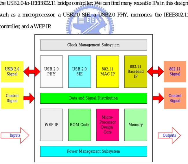
(13) Chapter 1. Introduction. 1.1 Reusable Intellectual Property In 1965, Gordon Moore noted that the number of transistors on a chip doubled every 18 to 24 months. Now, advance in silicon technology allows us to build chips consisting of tens of millions of transistors. The ability to leverage valuable intellectual property (IP) through design reuse will be the invariable cornerstone of any effective attack on the productivity issue. Reusable IP is essential to achieving the engineering quality and the timely completion of multimillion-gate ICs [1]. Figure 1.1 is an example of complex System-on-a-Chip (SoC) design. This design is the USB2.0-to-IEEE802.11 bridge controller. We can find many reusable IPs in this design, such as a microprocessor, a USB2.0 SIE, a USB2.0 PHY, memories, the IEEE802.11 controller, and a WEP IP.. Clock Management Subsystem. USB 2.0 Signal. USB 2.0 PHY. Control Signal. USB 2.0 SIE. 802.11 MAC IP. 802.11 Baseband IP. Control Signal. Data and Signal Distribution. WEP IP. ROM Code. Inputs. MicroProcessor Design Core. Memory. Power Management Subsystem. Figure 1.1 An example of complex SoC 1. 802.11 Signal. Outputs.
(14) 1.2 Built-In Self Test Technique for VLSI Design Testing has become a more difficult problem, due to increasing chip complexity over the past two to three decades. Especially, embedded core functions have become common in VLSI devices with the embedded nature of these functions, making them more difficult to test. In addition, more expensive test equipments are required to handle larger number of I/O pins, higher operating frequencies, and larger sets of test vectors, typically associated with the more complex VLSI device. Finally, due to the growing complexity of VLSI devices, the ability to provide some level of fault diagnosis during manufacturing testing is needed to assist failure mode analysis (FMA) for yield enhancement and repair procedures. Built-In Self Test (BIST) is considered to be one of the primary solutions to these predicted and growing testing problems. The basic idea of BIST is to design a circuit so that the circuit can test itself and determine whether it is fault-free or faulty. This typically requires additional circuitry and functionality to be incorporated into the circuit to facilitate the self-testing. This additional functionality must be capable of generating test patterns as well as providing a mechanism to determine if the output responses of the CUT to the test patterns agree to that of the fault-free circuit. A representative architecture of the BIST is illustrated in the block diagram of Figure 1.2. This BIST architecture includes two essential functions as well as two additional functions that are necessary to facilitate execution of the self-testing feature while in the system. These two essential functions include the test pattern generator (TPG) and the output response analyzer (ORA). While the TPG produces a sequence of patterns for testing the CUT, the ORA compacts the output responses of the CUT into some type of Pass/Fail indication. The other two functions needed for system-level use of the BIST include the BIST controller and the input multiplexers.. 2.
(15) Aside from the normal system I/O pins, the incorporation of BIST may also require additional I/O pins for activating the BIST sequence (the BIST Start signal), reporting the results of the BIST (the Pass/Fail indication), and an optional indication (BIST Done) that the BIST sequence is complete and that the BIST results are valid to be read to determine the fault-free/faulty status of the CUT [2].. BIST Done. BIST Start BIST Controller Test Pattern Generator. System Inputs. Output Response Analyzer. Input Mux. Circuit Under Test (CUT). Figure 1.2. Basic BIST architecture. Pass / Fail. System Outputs. 1.3 Purpose of This Thesis Because of the exponentially growing in wireless communications, many VLSI designers invest much time and resource in creating these components in wireless communications. However, at the same time, the eavesdropping is a familiar problem to users of any types of wireless communications. For this reason, there are many algorithms and architectures about encryption and decryption in wireless technology. In this thesis, we will design a reusable Wire Equivalent Privacy (WEP) IP for the secrecy requirement. The specification of WEP is defined in the IEEE 802.11 wireless standard. In order to guarantee the quality and ease to be reused, we will not only create a. 3.
(16) reusable WEP component but also design a built-in self test (BIST) circuit for this IP. We hope to devise a smart method to obtain the quality fault coverage with less effort.. 1.4 Outline of This Thesis This thesis is organized as follows. Chapter 2 presents the IEEE 802.11 Wire Equivalent Privacy standard and describes the architecture of the WEP IP. Chapter 3 presents the traditional testing methods for the WEP IP. Chapter 4 presents the new BIST design in the WEP IP. In chapter 5, conclusions are given.. 4.
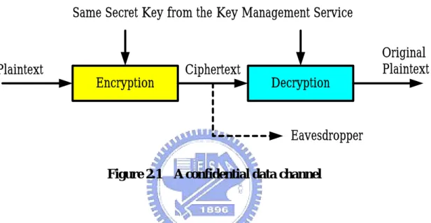
(17) Chapter 2. The Wired Equivalent Privacy (WEP) IP. Wired Equivalent Privacy [3]. 2.1. 2.1.1 Introduction Eavesdropping is a familiar problem to users of any types of wireless technology. IEEE 802.11 specifies an optional privacy algorithm “Wire Equivalent Privacy” that is designed to satisfy the goal of wired LAN “equivalent” privacy. The algorithm is not designed for ultimate security but rather to be “at least as secure as a wire”. The WEP algorithm has the following properties: 1.. It is reasonably strong because WEP allows for the changing of the key and frequent changing of the initialization vector (IV) to against the brute-force attack.. 2.. WEP is self-synchronizing for each message to reduce the packet loss rates.. 3.. The WEP algorithm is efficient and may be implemented in either hardware or software. 4.. The WEP algorithm may be exportable from the USA.. 5.. The implementation and use of WEP is an IEEE 802.11 option.. 2.1.2 WEP Theory of Operation Data that are not enciphered are called plaintext (denoted by P) and data that are enciphered are called ciphertext (denoted by C). The process of disguising (binary) data in order to hide their information content is called encryption (denoted by E) and the process of turning ciphertext back into plaintext is called decryption (denoted by D). The encryption function E operates on P to produce C: EK(P) = C. (1). 5.
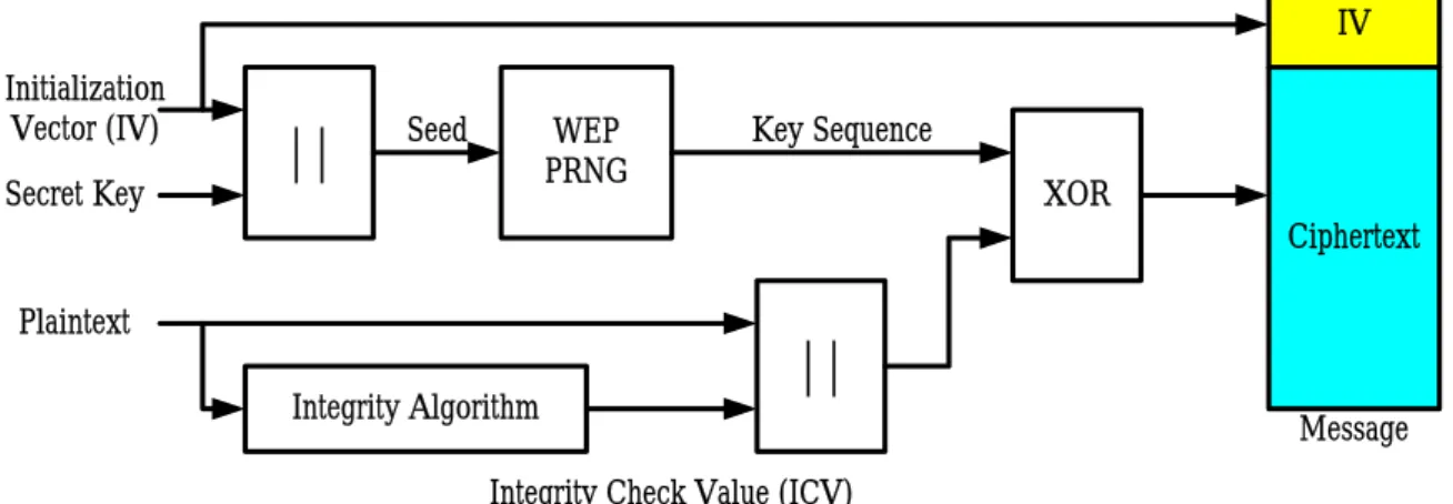
(18) In the reverse process, the decryption function D operates on C to produce P: DK(C) = P. (2). WEP is a symmetric algorithm in which the same key is used for encipherment and decipherment. We can get the following equation: DK(EK(P)) = DK(C) = P. (3). The procedure of encryption and decryption is depicted in Figure 2.1.. Same Secret Key from the Key Management Service. Plaintext. Ciphertext. Encryption. Original Plaintext Decryption. Eavesdropper Figure 2.1. A confidential data channel. Referring to Figure 2.2, the secret key is concatenated with an initialization vector (IV) and the resulting seed is input to a pseudo-random number generator (PRNG). WEP uses the RC4 PRNG algorithm as defined in Section 2.1.4. The PRNG outputs a key sequence k of pseudorandom octets equal in length to the number of data octets that are to be transmitted plus 4. The key sequence is used to protect the integrity check value (ICV) as well as the data. The WEP ICV is 32 bits. The WEP Integrity Check algorithm is CRC-32, as defined with the following equation: G(X)=X32+X26+X23+X22+X16+X12+X11+X10+X8+X7+X5+X4+X2+X1+1. (4). The encrypted ICV can guarantee the completeness of message and protect the ciphertext from malicious distortion. WEP combines key sequence k with plaintext using bitwise XOR to generate ciphertext. The output of the process is a message containing the IV and ciphertext. 6.
(19) IV Initialization Vector (IV) Secret Key. ||. Seed. Key Sequence. WEP PRNG. XOR Ciphertext. Plaintext. ||. Integrity Algorithm. Message. Integrity Check Value (ICV). Figure 2.2. WEP encipherment block diagram. Referring to Figure 2.3, decipherment begins with the arrival of a message. The IV of the incoming message shall be combined with the same secret key to generate the same seed as encipherment, as depicted in Figure 2.4. The same seed and the same PRNG algorithm generate the same key sequence to decipher the incoming encrypted message. Combining the ciphertext with the proper key sequence yields the original plaintext and ICV. The same integrity check algorithm is used to generate the ICV’ from the recovered plaintext. Correct decipherment shall be verified by comparing the output ICV’ to the ICV transmitted with the message. If ICV’ is not equal to ICV, the received message is in error and an error indication is sent to the management.. Secret Key IV. ||. Seed. WEP PRNG. Plaintext Key Sequence. Ciphertext. Integrity Algorithm ICV' (CRC-32). XOR ICV. Message. Figure 2.3. WEP decipherment block diagram. 7. ICV=ICV' ?.
(20) 63 / 127. 24 23 Secret Key [39:0] or Secret Key [103:0]. 0. Initialization Vector [23:0]. Figure 2.4 Format of the Seed = { Secret Key , Initialization Vector } 2.1.3 WEP Frame Body Expansion Figure 2.5 shows the encrypted Frame Body in general frame form as constructed by the WEP algorithm.. 2 Bytes. 2 Bytes. 6 Bytes. 6 Bytes. 6 Bytes. 2 Bytes. 6 Bytes. 0~2312 Bytes. 4 Bytes. Frame Control. Duration ID. Address 1. Address 2. Address 3. Sequence Control. Address 4. Frame Body. FCS (CRC-32). MAC Header Encrypted Data IV 4 Bytes. Data >= 0 Byte. ICV 4 Bytes. Not Encrypted Data 1 Byte Pad Key ID 000000 2 bits. Initial Vector 3 Bytes. Figure 2.5. Construction of expanded WEP Frame Body. The encipherment process has expanded the original Frame Body by 8 octets, 4 for the IV field and 4 for the ICV. The ICV is calculated on the data field only. The IV field shall contain three subfields: a three-octet field that contains the initialization vector, a 2-bit key ID field, and a 6-bit pad field. The initialization vector is a part of seed which was described in the early part of this chapter. The contents of the pad subfield shall be zero. 8.
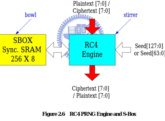
(21) The Key ID subfield contents select one of four possible secret key values for use in decrypting this Frame Body.. 2.1.4 RC4 PRNG Algorithm [4] WEP uses the “RC4 PRNG algorithm” which was originally from RSA Data Security, Inc. The RC4 PRNG is a stream cipher symmetric key algorithm. The transmitter and the receiver have same secret key sequence. Referring to Figure 2.6, a 256-byte RAM that is named substitution boxes (denoted by S-Box) contents 256 independent number in random order. The RC4 PRNG engine is like a stirrer to stir the random number in the S-Box.. bowl. Plaintext [7:0] / Ciphertext [7:0]. SBOX Sync. SRAM 256 X 8. RC4 Engine. stirrer. Seed[127:0] or Seed[63:0]. Ciphertext [7:0] / Plaintext [7:0] Figure 2.6 RC4 PRNG Engine and S-Box. There are two major steps in RC4 PRNG to initiate the S-Box then generate the key sequence. The first step is called “RC4 Seeding”. In this step, the RC4 PRNG engine uses the incoming seed to stir the order of number in S-Box. The algorithm of the “RC4 Seeding” is defined in following Figure 2.7:. 9.
(22) Defined: Key_Length = (bit number of valid Seed) / 8 Key [ x ] = Seed [ x * 8 + 7 : x ] ; where 0 ≦ x ≦ 15 S [ y ] is the octets in the S-Box at address y ;. where 0 ≦ y ≦ 255. RC4 Seeding: For ( I = 0 ; I < 256 ; I = I + 1 ) S [ I ] = I; For ( I = J = 0 ; I < 256 ; I = I + 1 ) { J = J + S [ I ] + Key [ ( I. modulo. Key_Length ) ] ;. SWAP ( S [ I ] , S [ J ] ); } I = J = 0;. Figure 2.7. RC4 Seeding equation. The second step is “Generate Key Sequence”. The RC4 PRNG engine continuously generates 8-bit key sequence of pseudorandom octets equal in length to the number of data octets that are to be transmitted plus 4. In the encipherment process, WEP combines key sequence with plaintext using bitwise XOR to generate ciphertext. In the decipherment process, the plaintext is recovered from the same key sequence and incoming ciphertext. When an octet key sequence is generated, the RC4 PRNG engine stirs the order of number in S-Box again. The algorithm of the “RC4 Generate Key-stream” is defined in following Figure 2.8:. 10.
(23) RC4 Generate Key Sequence : I = ( I + 1 ) modulo 256; J = ( J + S [ I ] ) modulo 256; SWAP ( S [ I ], S [ J ] ); Key Sequence [ 7 : 0 ] = S [ ( S [ I ] + S [ J ] ) modulo 256 ];. Figure 2.8. 2.2. RC4 Generate Key Sequence equation. Designing a Reusable WEP IP In the second part of Chapter 2, our target is to design a reusable WEP IP based on. IEEE 802.11 standard and RC4 algorithm described in the early part of this chapter.. 2.2.1 Design Flow Before to deign a “Build-In Self Test (BIST)” circuit for WEP IP, we must design a reusable WEP IP based on standards. To finish a reusable WEP IP, there are some major steps of design shown in Figure 2.9. In this figure, the EDA tools used for developing the WEP IP are also shown beside the blocks of steps with blue text [5, 6, 7, 8]. The first step is “specification definition”. Every design needs a target specification to point out the features and the applications. The detail specification of WEP IP is defined in Section 2.2.2. The second step is “RTL coding of WEP IP”. In this step, the architecture and the block diagram of “WEP IP” are depicted. Because the WEP IP is a synchronous and synthesizable design, we create the “Register Transfer Level” (denoted by RTL) code in the “Verilog Hardware Description Language (HDL)”. The third step is “RTL simulation of WEP IP”. There are two simulation cases to. 11.
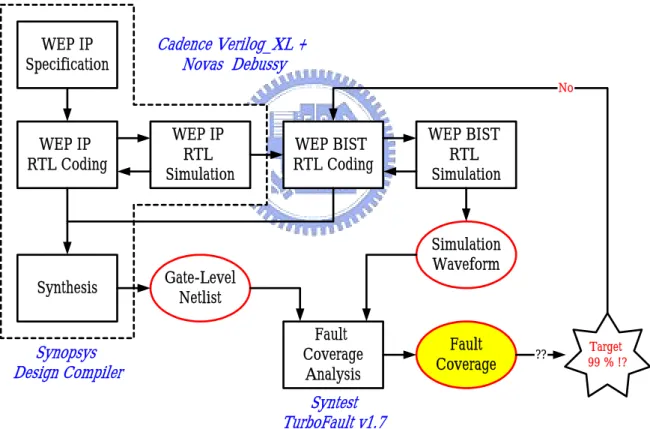
(24) verify the correctness of the WEP encipherment and the decipherment. These simulation environments and patterns are also created in Verilog HDL. If there are any mismatch or incorrectness, we will return to step 2 to modify the RTL code and to fix the issue. Please refer to Section 2.2.4 for the waveforms of simulations. After all simulations are passed successfully, the RTL code will be synthesized to gate level netlist with a target process. We use the tsmc 0.35um process in this paper. In this step, we also do the timing and area optimization with synthesis EDA tools. Please refer to Section 2.2.5 for the synthesis constraints and results.. Cadence Verilog_XL + Novas Debussy. WEP IP Specification. No. WEP IP RTL Simulation. WEP IP RTL Coding. WEP BIST RTL Coding. Simulation Waveform. Gate-Level Netlist. Synthesis. Synopsys Design Compiler. WEP BIST RTL Simulation. Fault Coverage Analysis. Fault Coverage. ??. Target 99 % !?. Syntest TurboFault v1.7. Figure 2.9. The Design Flow of the WEP IP with BIST. When the gate level netlist of WEP IP is ready, we begin to design a BIST circuit for this IP. The same design flows described below are also followed, for us to create the BIST module for the WEP IP. Please refer to Chapter 4 for the detail description of the BIST. 12.
(25) design for the WEP IP. 1. Define the architecture and create the RTL code of BIST. 2. Pass the simulations of the full IP including WEP IP and BIST. 3. Synthesize and transfer all RTL codes to gate level netlist. 4. Simulate and verify the “Fault Coverage” of WEP IP with the gate level netlist and simulation patterns. The BIST module has to be re-structured and re-deigned until we get an approved “Fault Coverage”.. 2.2.2 Specification This “WEP IP” is a reusable intellectual proprietary (IP) for IEEE 802.11a/b wireless network decrypting and encrypting function. Because of the embedded PRNG and CRC-32, this module can be a platform for “Design for Test” verification of NCTU VLSI Testing Lab. The features of this WEP IP are described in below: A reusable independent Wired Equivalent Privacy (WEP) decryption and encryption module for IEEE 802.11 a/b. Fully compatible IEEE 802.11 a/b WEP specification. Embedded RC4 decrypt and encrypt algorithm. Supply both 64 and 128 secret keys. Built-in one 256 bytes synchronous SRAM for S-Box. A half-duplex module. Only decrypt mode or encrypt mode can be enabled at a time. The maximal operating frequency is 125MHz with 0.35um processing. The maximal latency to encrypt or decrypt is 6 system clocks. In other words, the maximal through rate is 166.67 Mbps. Provide a high performance Built-in Self Test module in this IP. 13.
(26) In order to verify this IP with a single chip, we specify a few pin count assignment as defined in Table 2.1. The last three pins, “BIST_Mode”, “BIST_Good”, and “BIST_End” are defined for BIST mode. Please refer to chapter 4 for BIST mode.. Name. I/O. Function Description. Clock. I System Clock, The maximal working frequency is 125MHz.. Reset. I. Mode_Sel. System Reset, Active High, The active width must larger than two clock periods.. I Mode select signal; 1 : Encrypt Mode, 0 : Decrypt Mode. Din[7:0]. In decrypt mode, Din[7:0] are the secret key, ciphertext, and the I encrypted ICV data bus input. In encrypt mode, Din[7:0] are the secret key, and plaintext input.. Din_STB. I Input data (Din[7:0]) valid strobe pulse. Active High. Key_Sel. I When “Key_Sel” is active, the “Din[7:0]” is secret key input.. Data_Sel. I. When “Data_Sel” is active, the “Din[7:0]” is ciphertext input in decrypt mode or plaintext input in encrypt mode.. ICV_Sel. I. This signal is only active in decrypt mode when the ICV data is valid on Din[7:0].. Dout[7:0]. O. In decrypt mode, Dout[7:0] are plaintext output. In encrypt mode, Dout[7:0] are ciphertext and the encrypted ICV output.. Dout_STB O Output data (Dout[7:0]) valid strobe pulse. SBox_RDY O. This signal is active when the RC4 seeding is done and the S-Box is ready to generate the key sequence.. In decrypt mode, “WEP_ICVo” is the flag to show the ICV comparing WEP_ICVo O result. In encrypt mode, the Dout[7:0] are the encrypted ICV output when “WEP_ICVo” is active. WEP_ERR O. This signal is active when the WEP procedure is stopped with any error. The signal will be cleared automatically while the procedure is restarted.. BIST_Mode I Set “BIST_Mode” to enable the BIST mode. BIST_Good O The BIST result, “1” is passed and “0” is failed. BIST_End. O The BIST procedure is done when this signal is set. Table 2.1. The pin description of WEP IP. 14.
(27) 2.2.3 Architecture Referring to Figure 2.10 “The Block Diagram of WEP IP”, the top level is named “WEP_IP”.. All input signals are at the left side, and all output signals are at the right. side. There are two major blocks in “WEP_IP”. The green block is a synchronous SRAM 256 X 8. This is an unsynthesisable behavioral model. Being the S-Box of WEP, this module stores the secret keystream for WEP encryption or decryption. The behavior model is only for simulation. This module is impossible to be synthesized by the synthesis tools, such as “Synopsys Design Compiler” at the present stage. In the real chip implementation, we can use the “Memory Compiler” EDA tools provided by foundries or custom design circuit and layout to generate this memory macro.. WEP_IP. Sync. SRAM 256X8 S-Box. WEP_CORE Dout[7:0] WEP_PRNG. Din[7:0]. SBox_RDY. Din_STB Mode_Sel. Dout_STB. WEP_RX. Key_Sel. WEP_ICV. Data_Sel WEP_CRC. ICV_Sel. WEP_ICVo. WEP_ERR Figure 2.10. The Block Diagram of WEP IP. In “WEP_IP”, the yellow block is called “WEP_CORE”. This module is the top level 15.
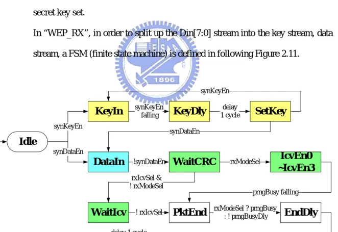
(28) of all synthesizable logic circuits. All input and output signals are also connected with this module. We divide “WEP_CORE” into three sub-modules by functions. The first one is named “WEP_RX”. “WEP_RX” is entrance module of “WEP_CORE”. It manages three major functions described as follows: “WEP_RX” synchronizes all external input signals with the internal clock and transfers them to other sub-modules to avoid all unexpected timing violation in RTL design, such as metastability violation. “WEP_RX” also collects the 64/128 bits secret key from the Din[7:0] bus. It will set a “secret key ready” signal to inform “WEP_PRNG” when received a correct secret key set. In “WEP_RX”, in order to split up the Din[7:0] stream into the key stream, data stream, a FSM (finite state machine) is defined in following Figure 2.11.. synKeyEn. KeyIn. synKeyEn falling. synKeyEn. delay 1 cycle. KeyDly. SetKey. synDataEn. Idle synDataEn. DataIn. !synDataEn. WaitCRC. rxModeSel. rxIcvSel & ! rxModeSel. WaitIcv. ! rxIcvSel. IcvEn0 ~IcvEn3. prngBusy falling. PktEnd. rxModeSel ? prngBusy : ! prngBusyDly. EndDly. delay 1 cycle. Yellow Blocks : Key Stream Input Green Blocks : ICV Stream Input. Blue Blocks : Data Stream Input White Blocks : Control Block. Figure 2.11 The FSM of WEP_RX. 16.
(29) The second sub-module in “WEP_CORE” is named “WEP_PRNG”. As implied in the name, “WEP_PRNG” is the kernel to generate a pseudo-random number with the RC4 algorithm as defined in Section 2.1.4. The main FSM of “WEP_PRNG” is defined in Figure 2.12 below.. ! btMem & &cntI delay 8 cycles. Idle. btMem &&cntI. Init. MemBist. !mBistFlag &&cntI. 1 cycle. WaitKey. rxKeyRdy. ReadSI. 1 cycle. WriteSJ. 1 cycle. WriteSI. else. delay 1 cycle. B CalcJ. mBistFlag &&cntI. ReadSJ. &cntI or btFast. Yellow Block : for (I=0;I<256;I++) S[I] = I;. &cntI or btFast. A. Green Block : SRAM BIST for (I=0;I<256;I++) { S[I] = I; Read and compare; } for (I=0;I<256;I++) { S[I] = 256 - I; Read and compare; }. GetSI. 1 cycle. Blue Block : for (I=J=0;I<256;I++) { J = J+S[I]+Key[I%Key_Length]; SWAP (S[I], S[J]); } I = J = 0;. NewJ. 1 cycle. A. GetSJ. dataRdy dataRdy. WaitData. else. GetKey. 6 cycles = Encrypt/Decrypt Latency. 1 cycle. UpdateSI. 1 cycle. prngErr or rxEndFlag. B. Red Block : I = (I+1) % 256; J = (J+S[I]) % 256; SWAP (S[I],S[J]); Key = S[(S[I] + S[J]) % 256];. Figure 2.12 The FSM of WEP_PRNG 17. UpdateSJ. 1 cycle.
(30) The comment text on Figure 2.12 is the equation of the RC4 PRNG algorithm. In the general function, “WEP_PRNG” will find out the secret key from the S-Box and generate the encrypted or decrypted data with the input data. For this reason, the other duty of “WEP_PRNG” is to control the S-Box (a Sync. SRAM 256x8). The third sub-module in “WEP_CORE” is named “WEP_ICV”. In the decryption mode (Mode_Sel = 0), the “WEP_ICV” checks the 32 bits ICV input data decrypted from the “WEP_PRNG” module and set the “WEP_ICVo” signal when the ICV check is successful. In the encryption mode (Mode_Sel = 1), the “WEP_ICV” transfers the CRC-32 output data to “WEP_RX” module. Then, “WEP_RX” transfers this CRC-32 data to “WEP_PRNG” module to generate the encrypted ICV output data.. 2.2.4 Simulation Results Referring to Figure 2.13, the flowchart in the left side is the procedure of WEP encryption and the comments in the right side are conditions of this procedure.. Reset & Encrypt Mode. Mode_Sel = 1. Secret Key Input (64/128 bits). Key_Sel = 1 with Din_STB =1. Wait RC4 Seeding. wait SBox_RDY = 1. Plaintext --> Ciphertext. Data_Sel = 1 with Din_STB = 1, Ciphertext ready when Dout_STB. ICV output. Icv_Sel = 1 with WEP_ICVo, ICV data ready when Dout_STB. Figure 2.13. The WEP encrypt procedure. 18.
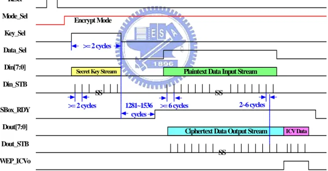
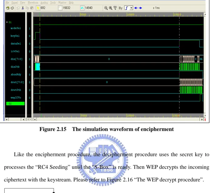
(31) As soon as “WEP_RX” receives the complete secret key from the external application circuit, “WEP_PRNG” processes the “RC4 Seeding” until the “Sbox_RDY” signal is set. This process takes 1536 cycle time. Setting “Sbox_RDY” means that the process of “RC4 Seeding” is finished and the “S-Box” is ready for encipherment or decipherment process. For the red blocks in Figure 2.12 “The FSM of WEP_PRNG”, there are six steps to transfer an incoming plaintext to a ciphertext. For this reason, the latency delay to encrypt or decrypt a byte is six cycles time. We can find out the encryption procedure and the timing relationship on Figure 2.14 “The encrypt chart” and Figure 2.15 “The simulation waveform of encipherment”.. Reset Mode_Sel. Encrypt Mode. Key_Sel Data_Sel Din[7:0]. >= 2 cycles. Plaintext Data Input Stream. Secret Key Stream. Din_STB. SS SBox_RDY. >= 2 cycles. SS 1281~1536 cycles. Dout[7:0]. 2~6 cycles. >= 6 cycles. Ciphertext Data Output Stream. Dout_STB. SS WEP_ICVo. Figure 2.14. The encryption chart. 19. ICV Data.
(32) Figure 2.15. The simulation waveform of encipherment. Like the encipherment procedure, the decipherment procedure uses the secret key to processes the “RC4 Seeding” until the “S-Box” is ready. Then WEP decrypts the incoming ciphertext with the keystream. Please refer to Figure 2.16 “The WEP decrypt procedure”.. Reset & Decrypt Mode. Mode_Sel = 0. Secret Key Input (64/128 bits). Key_Sel = 1 with Din_STB wait SBox_RDY = 1. Wait RC4 Seeding. Data_Sel = 1 with Din_STB = 1 Plaintext ready when Dout_STB. Ciphertext --> Plaintext. If ICV check correctly, WEP_ICVo = 1. check ICV Figure 2.16. The WEP decrypt procedure. 20.
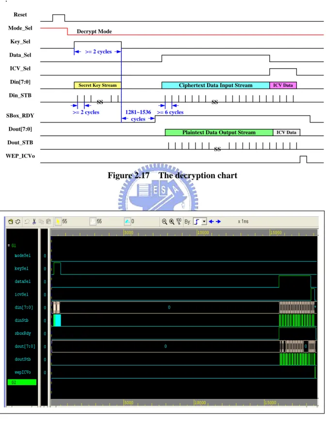
(33) Figure 2.17 shows the decryption chart in an ideal case. Figure 2.18 shows the simulation waveforms of decipherment . Reset Mode_Sel. Decrypt Mode. Key_Sel Data_Sel. >= 2 cycles. ICV_Sel Din[7:0]. Ciphertext Data Input Stream. Secret Key Stream. ICV Data. Din_STB SS SBox_RDY. >= 2 cycles. SS 1281~1536 cycles. >= 6 cycles. Dout[7:0]. Plaintext Data Output Stream. Dout_STB SS WEP_ICVo. Figure 2.17. Figure 2.18. The decryption chart. The simulation waveform of decipherment. 21. ICV Data.
(34) 2.2.5 Synthesis Results After passed all simulations in RTL design, we synthesis this WEP IP from Verilog RTL code to the tsmc 0.35um process standard cell netlist with the Synopsys EDA tool “Design Compiler”. The synthesis results are described in Table 2.2 below. Process: tsmc 0.35 standard cell library (cb35os142) Area: Logic = 4139 gate count. (1 gate = 1 2-input NAND cell). Marco = The synchronous SRAM 256x8 The maximal operating frequency = 125MHz in the worst case The critical path is the path from SRAM data output to “WEP_PRNG” sub-module. Table 2.2. The synthesis results of the WEP IP. 2.3 Summary In order to implement our BIST method in a general digital design, we follow the reuse methodology of VLSI IP to finish an optimal WEP IP based on the IEEE 802.11 standard. In this chapter, we have described the detail specification, pin assignment, architecture and the FSM of each sub-module in our WEP IP design. We also go through simulations and the synthesis to create the WEP IP as a platform for BIST design in our later thesis.. 22.
(35) Chapter 3. Traditional Testing Methods for WEP IP. For design or product engineers, how to verify the function and guarantee the quality of chips is an important topic. There are many theories and methods which such as functional testing, and scan chain testing can help engineers to verify or test their chips. In this chapter, we will describe how to use these two traditional testing methods to test the WEP IP.. 3.1 Functional Testing The first traditional testing method for the WEP IP is “functional test”. A functional test is used to verify that the model or logic behavior as it was intended in specifications. A functional test is application of functional, operational, or behavioral vectors to the circuit under test. If the vectors are not evaluated for their structural coverage, then the vectors are generally referred to as “design verification” vectors. Section 3.1.1 describes the generating flow of the WEP IP’s functional patterns. Many designers still rely on functional vectors to accomplish the manufacturing, or product test. A functional test could be a good choice if the device is small or if the majority of the functional vectors exist from a previous but similar design. However, there are several problems with the use of functional vectors for any kind of manufacturing test on the modern VLSI design. First, functional vectors are very good for determining behavior, but are not especially good or efficient for structural verification. Second, functional vectors must be evaluated to verify the structural fault coverage. This is an extra and difficult task. In most cases, the fault coverage of functional vectors is very difficult to achieve the required quality level.. 23.
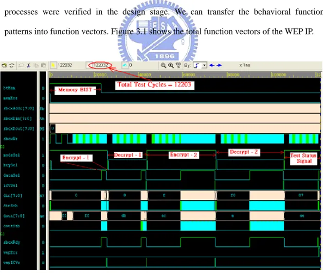
(36) Third, functional vector are designed to verify circuit behavior, and they are not as efficient as “deterministic” structural vectors. In modern SoC and VLSI designs, the test data volume is becoming a critical issue of the test cost. More test time and on-board memories are requested to achieve the expected quality [9]. Finally, the tester’s working frequency limits the maximal operating frequency of the functional vectors. In some cases, an engineer needs more expensive tester to verify his chips at-speed.. 3.1.1. Flow of Function Pattern Generation. As in the description in Chapter 2, the WEP IP is an independent reusable privacy module and its logic behavior is intended in specifications. Both encryption and decryption processes were verified in the design stage. We can transfer the behavioral function patterns into function vectors. Figure 3.1 shows the total function vectors of the WEP IP.. Figure 3.1. The WEP IP simulation waveform of functional vectors 24.
(37) The first stage of the functional test vector is “Memory BIST” to verify the embedded 256-bytes SRAM. We use some design skills to reduce the extra gate count for the memory BIST logic. Please refer to Section 3.1.2 for more detailed description. The second and the third stages are “Encrypt 1” and “Decrypt 1” to verify the encryption and decryption function with a 64-bits secret key. In order to achieve the expected quality, the extra “Encrypt 2” and “Decrypt 2” stages are added into the procedure. Both these two processes are verified with a 128-bits secret key. At the last stage “Test Status Signal”, we try to trigger all status output signals with some expected conditions and function patterns to verify these ports. Finally, we must collect and transfer these function patterns into the test vectors that base on the types of test mechanisms. In order to reduce the length of test vectors, the data compression such as RZI and NRZI is also necessary. Figure 3.2 shows an example of test vectors without compression. crbdddddddddmkdidddddddddwwsm 1011000000001100HLHLLLHLLLLLL letiiiiiiiiioeacoooooooooeebe 1011000000011100HLHLLLHLLLLLL ksMnnnnnnnnndytvuuuuuuuuuppom 1011000000001100HHHLLHHLLLLLL ee01234567SeSaStttttttttEIxE 1010000000001100HLLHLLLHLLLLL tSeSe01234567SrCRr 1010000000011100HLLHLLLHLLLLL tm belel trVdr 1010000000001100LLLLLLLLLLLLL l l b oy 1010000000001000LLLLHHHLLLLLL 1010000000001000HLLLHHHLLLLLL 1110000000001000LLLLLLLLLLLLH 1010000000001000LHLLHHHLLLLLL 1011001000111100LLLLLLLLLLLLH 1010000000001000HHLLHHHLLLLLL 1011001000101100LLLLLLLLLLLLH 1010000000001000LLHLHHHLLLLLL 1011110011001100LLLLLLLLLLLLH 1010000000001000HLHLHHHLLLLLL 1011110011011100HLLHLLLHLLLLL 1010000000001000LHHLHHHLLLLLL 1011110011001100LLLLLLLLLLLLL 1010000000001000HHHLHHHLLLLLL 1010000000001100HLLLLLLLLLLLL 1010000000001000LLLHHHHLLLLLL 1010000000011100HLLLLLLLLLLLL 1010000000001000HLLHHHHLLLLLL 1010000000001100HHLLLHLLLLLLL 1010000000001000LHLHHHHLLLLLL 1011001000101100HLHLLLHLLLLLL 1010000000001000HHLHHHHLLLLLL 1011001000111100HLHLLLHLLLLLL 1010000000001000LHHHHHHLLLLLL 1011001000101100HHHLLHHLLLLLL 1010000000001000HHHHHHHLLLLLL 1011110011001100HLLHLLLHLLLLL 1010000000001000LLLLLLLHLLLLL 1011110011011100HLLHLLLHLLLLL 1010000000001000HLLLLLLHLLLLL 1011110011001100LLLLLLLLLLLLL 1010000000001000LHLLLLLHLLLLL Figure 3.2. A test vector example without compression. 25.
(38) In Figure 3.2, “1”, “0”, or “Z” are the symbols for the inputs when they are “high”, “low” or “high-impedance” respectively and “H”, “L” or “X” are the symbols for the outputs when they are “high”, “low” or “unknown” respectively.. 3.1.2. Testing for Embedded Memory. In the WEP IP, there is an embedded memory. This section describes how to use the traditional testing method to verify the embedded 256-bytes SRAM. In the modern SoC design, the topic of memory testing is not limited to just testing the embedded memory by using a tester. Three common test methods can be applied to verify the embedded memory. These test method options are: Embedded Microprocessor Access; Direct Memory Access by Tester; and Memory Built-in Self Test (MBIST). Each of these methods has trade-offs that involve: cost-of-test, chip area, chip pin requirements, chip-level timing and chip power requirements [9]. In our design, we implement an MBIST into the WEP IP to verify the embedded SRAM. Considering the extra area overhead, we prefer the “MATS” [10] algorithm and try to combine the MBIST controller with the original logic. As everyone knows, the “MATS” is the simplest algorithm to verify a memory. The “MATS” algorithm is described as follows:. (5) Every cell of the memory is written both value “0” and “1” and is read and verified. So the “MATS” can verify all stuck-at faults (SAF) in memory cells and some address decode faults (AF). The complexity of “MATS” is 4n. In our design, we need extra 1024 cycles to test the embedded 256-bytes SRAM with the “MATS” algorithm. In order to reduce the extra area and test time in MBIST, we try to combine this “MATS” algorithm with the original logic. First, we review the formula for RC4 described in Section 2.1.4. The first step of “RC4 Seeding” is defined as follows: 26.
(39) For ( I = 0 ; I < 256 ; I = I + 1 ) S [ I ] = I;. (6). We can transfer equation (6) above into equation (7) below.. { ↑ ( W (Address) ); }. (7). If we hope to combine the “MATS” and “RC4 Seeding” algorithm to reduce the extra gate-count and test time, we must add equation (8) below into our MBIST procedure.. (8) Because the address range of the WEP IP’s embedded 256-bytes SRAM is from 00h to FFh, we can use the same 8-bit address counter to generate both address and data for the test algorithm. Then, we can re-define the “MATS” MBIST algorithm as the following equation (9).. In equation (9) above, we can find equation (7) that is described in the red text. So, we can merge the “MATS” and the FSM of RC4 PRNG to save test time of equation (7). By the way, we can reuse the same address counter that originally existed in “WEP_PRNG” module to generate the test address and data for the “MATS”. As shown in Figure 2.12, the “Memory BIST” state is inserted between the “Initial” and “Wait Secret Key” state. In order to avoid the redundant MBIST process, we also create a status signal “mBistFlag” to record the MBIST procedure. If this status signal is set, the FSM will bypass the “Memory BIST” state to guarantee that only one MBIST cycle will be done. In summary, this MBIST algorithm is good to save extra gate-count and test time. There are only 284 gates extra to build up this “MATS”-comparable MBIST in the WEP IP.. 27.
(40) However the low fault coverage of the “MATS” algorithm is its drawback. We will re-design a “14N MARCH C+” MBIST into our WEP BIST that will be described in Section 4.2.4.. 3.1.3 Fault Coverage Results As described in Figure 2.9 “Design Flow of WEP IP with BIST”, we used the EDA tool “Syntest TurboFault” [8] to fault simulate the WEP IP with the patterns described in Section 3.1.1 to evaluate the fault coverage. The fault coverage report for those functional test vectors are shown in Table 3.1. Item. Number. Percentage. Optimal Fault Coverage. --. 92.69 %. Total Faults. 13042. 100.00 %. Hard Detected Faults. 11106. 85.16 %. Probably Detected Faults. 983. 7.54 %. Undetected Faults. 950. 7.28 %. Table 3.1 WEP IP fault coverage report with functional test vectors. The total testing time is 12203 clock cycles. In other words, if the tester operating frequency is 10MHz, it will take about 1.22 ms to finish the procedure. The total gate count is 4454 gates. To compare the gate count with the WEP IP gate count described in Table 2.2, the area overhead is 315 gates, almost 7.07 %. The extra gate count was caused of the MBIST controller described in the last section. In order to improve the fault coverage, additional functional patterns such as “Encrypt 2” and “Decrypt 2” must be included.. 28.
(41) 3.2 Test Method by Scan-Chain Because “higher frequency”, “higher pin-count”, “higher levels of integration”, and “higher complexity” drive up the cost of the test platforms required to test modern chips, the scan-based testing is famous in modern SoC design. Today, there are many EDA tools, which can help designers to insert scan-chains and generate effective vectors for their chips. So we use the Syntest’s EDA tool “TurboScan” [11] to generate the scan-chain in our WEP IP and discuss the advantages and disadvantages in different design styles. For an embedded module or IP in a SoC design, there are many testing problems, which must be solved when a scan-chain is to be inserted into this IP. 1.. If the IP is a black-box and hard-macro, end-users can not directly control and observe the internal nets of the embedded module. It is impossible to verify this IP with scan-chains to get its fault coverage report.. 2.. If the IP is a firm-macro, i.e. a pure gate-level netlist, end-users cannot re-synthesize and insert the scan-chains because of the timing issues.. In next sections, we will describe and analyze the three scan-chain methods implemented in the WEP IP.. 3.2.1. ATPG with a WEP Hard-Macro. What is a hard-macro? A hard-macro is a black-box in VLSI design that end-users can not control and observe its internal nets and can not insert the scan-chain into these unknown logic. The IP provider can provide a hard-macro IP with local scan-chain. But there are many uncontrollable parallel inputs (PI) and unobservable parallel outputs (PO) in the hard-macro IP, as described in Figure 3.3 below. Unfortunately, these uncertain PI and PO will cause low fault coverage as shown in Table 3.2.. 29.
(42) A SoC Design with Scan-Chains SO [1]. SI [1]. PO. PI. SO [2]. SI [2] Custom Logic and Modules Test_Mode Scan_Enable. SI [3]. ?. ?. PI. PO. ?. PI. SO [3]. ?. ?. ?. PO. ? WEP Core. Local Scan-Chain. ?. ?. Embedded 256x8 SRAM. WEP IP Figure 3.3. Local Scan-Chain in a Hard-Macro IP. Fault Coverage. 79.49 %. Test Patterns. 66. Total Gate-Count. 4836. Chain Length. 305. Area Overhead. 14.41 %. Estimated Cycles. 20632. Table 3.2. Fault coverage report of the Hard-Macro WEP IP. 30.
(43) 3.2.2 ATPG on WEP IP without Memory Wrapper If we provide the WEP IP RTL code or the gate-level netlist to end-users, the end-user can implement his scan-chains into all logic including “WEP_CORE”. Because the WEP IP includes an embedded memory array, the memory looks like a large “blocked area” within a scan logic test area. Everything in the downstream of the memory may experience a loss of controllability because the output from the memory array is unknown.. A SoC Design with Scan-Chains SO [1]. SI [1]. PO. PI. SO [2]. SI [2] Custom Logic and Modules Test_Mode Scan_Enable PI. PO. SI [3]. SO [3] PO. PI WEP Core ?. ?. Embedded 256x8 SRAM. WEP IP Figure 3.4. ATPG on WEP IP without Memory Wrapper 31.
(44) Please refer to Figure 3.4 above, we can find that all signals connected with the embedded SRAM are uncontrollable and unobservable. If we leave this large “blocked area” in the WEP IP, the low quality fault detection is expected as Table 3.3.. Fault Coverage. 90.22 %. Test Patterns. 87. Total Gate-Count. 4836. Chain Length. 305. Area Overhead. 14.41 %. Estimated Cycles. 27100. Table 3.3. Fault coverage report of the WEP IP without Memory Wrapper. 3.2.3 ATPG on WEP IP with Memory Wrapper In order to get as much coverage of the area between the scan architecture and the memory test architecture, several methods are used for the interaction of a memory with a general chip scan logic. The most general method is to insert a memory wrapper to isolate the “blocked area” from scan-chains, as illustrated in Figure 3.5 [9].. Scan Out Data In. Din. Address. Memory Array Addr in ATPG. Control. RD/WR. Dout. Scan In. Figure 3.5. Memory Wrapper in ATPG 32. Data Out.
(45) In modern digital design methods, most ATPG EDA tools have the ability to handle memory interaction automatically. In our WEP IP, we try to insert the memory wrapper by designing some extra circuit to string the inputs and outputs of the embedded SRAM as described in Figure 3.5. There are totally 25 flip-flops and 25 multiplexers for the memory wrapper. In order to isolate the memory macro from the scan-chain, these unavoidable wrapper cells are the extra area overhead. The fault coverage report of the ATPG with the memory wrapper is described in Table 3.4.. Fault Coverage. 98.91 %. Test Patterns. 101. Total Gate-Count. 5124. Chain Length. 330. Area Overhead. 19.22 %. Estimated Cycles. 33962. Table 3.4. Fault coverage report of the WEP IP with Memory Wrapper. We get an exhilarating fault coverage report with this ATPG method. The area overhead is 19.22% because the total gate-counts of the WEP without MBIST are only 4139. If we only consider the area overhead of the scan-chain and memory wrapper in this design, the original gate-count of the “WEP with MATS MBIST” is 4423. So, the pure area overhead of the scan-chain with memory wrapper is almost 14%. In summary, for a small design, the ATPG area overhead is appreciable.. 3.3 Summary Usually, designers do not pay much attention to take care the testing issues during the design phase. They always try to finish their design on specification and on schedule then leave these testing problems to functional vectors or ATPG EDA tools. Undoubtedly, most ATPG EDA tools can handle the full-chip scan smartly and effectively. Here scan vectors. 33.
(46) are more efficient than functional vectors, and a higher fault coverage report can be obtained. However, the full scan still has some disadvantages and limitations as follows. 1. The scan method cannot reach an embedded “blocked area”, such as embedded memories and a hard-macro IP. 2. A designer must handle the clock skew issue on the scan clocks when the scan clocks string many different clock domains. An extra effort and extra area overhead should be paid to fix these timing violations caused by these different clock delays. 3. In order to reach the quality level fault coverage, the number of ATPG patterns and the testing cycles are appreciable. For an IP design, it is impossible to prepare a larger of memory to store these test vectors in the built-in self test circuit. This is why we try to design a BIST module in the WEP IP without any memory storage.. 34.
(47) Chapter 4. A Built-In Self Test Design for WEP IP. Because there are many disadvantages and limitations when implementing an effective testing method into the independent IP, we would like to design a BIST circuit to qualify the WEP IP.. Features. 4.1. Refer to the disadvantages and the advantages of the traditional testing methods described in Chapter 3, we work out the features of the BIST module as follows. 1.. This BIST module can provide the high fault coverage for our WEP IP. The target fault coverage value is 99%.. 2.. It provides an at-speed testing method to detect delay faults in circuit. The target operating frequency is 125MHz in 0.35um process.. 3.. Only a few of extra pin must be provided for the BIST module. In other words, a friendly interface is necessary.. 4.. The BIST module will generate the testing patterns and check the correctness automatically. There is no extra memory to store the vectors.. 4.2. 5.. Use the least pattern to meet these features above.. 6.. Use the least extra gate-count to create this BIST module.. Description of the BIST for WEP IP In this section, we describe the general idea and the method of the BIST design. 4.2.1 Architecture Referring to Figure 4.1 below, the general idea of the testing method is to design an. extra external BIST module to generate and multiplex the input signals that are transferred 35.
(48) to the WEP IP. The BIST module not only generates and feed the testing vectors into the WEP IP, it also collects and calculates the output signals from the WEP IP to verify the checksum value. If the calculated value matches with the golden pattern that was stored in the BIST module, the “BIST_Good” signal will be set to show the result. In Figure 4.1, the top module is named “weptop”. The “weptop” includes three sub-modules, the “WEP_IP” (wepip), the “WEP_BIST” (wepbist), and the “WEP BIST Clock Controller” (wepbtclk). The WEP IP was introduced in Chapter 2. In the next section, we will give a detailed description about the “WEP BIST” design. The major function of the “WEP BIST Clock Controller” is to disable the clock source to save the power in the normal mode. We will describe this module in Section 4.3.1. Output Signals. weptop bist Mode. wepbtclk. wepip. wepbist. Sync. SRAM 256 x 8. wepcore. wepcrc16. wepprng. wepicv. Golden Pattern. Input Signals bist End. weprx. wepbc. wepcrc. bist Good. Figure 4.1. The block diagram of the WEP IP with the BIST module. Figure 4.2 describes the data flow of the “WEP_IP” in the normal operation mode (bist_mode = 0). “WEP_BIST” bypasses the input data and does not cause any influence on the WEP_IP’s function during the normal operation mode.. 36.
(49) wepip. wepbtclk. bist_mode = 0 1. 1. btReset. SSRAM256x8. 0. btClk bistEnable. Normal Data In. wepcore wepbc. bist_End = 0. wepcrc16. bist_Good = 0. Normal Data Out. wepbist. weptop. Figure 4.2 The WEP IP data flow in the normal operation mode. Figure 4.3 describes the data flow of “WEP_IP” in BIST mode (bist_mode = 1). “WEP_BIST” generates all inputs of “WEP_IP” and compares the outputs from “WEP_IP” with a golden checksum which is stored in “WEP_BIST”.. wepip. wepbtclk. bist_mode = 1 0. SSRAM256x8. 1. btReset. btClk bistEnable. Normal Data In. wepcore bist_End = 0 -> 1. bist_Good = 0 -> 1. wepbc. wepcrc16. Normal Data Out. wepbist Figure 4.3. weptop. The WEP IP data flow in BIST operation mode 37.
(50) 4.2.2 Testing Method In this section, we focus on the function description of the WEP BIST method. The general idea of the BIST module is to design an automatic functional patterns generator to feed the WEP IP with some expected vectors. At the same time, this BIST module checks the output signals from the WEP IP then exports the testing result. In order to generate the testing vectors and ensure the normal functions, we design many multiplexers to select the WEP IP’s input data between the normal signals and the BIST vectors. Please refer to Figure 4.4 below. While the “BIST_Mode” signal, described in Table 2.1, is set, the “WEP BIST Clock Controller (wepbtclk)” sets the “bist_Enable” signal to active the select signal of the multiplexers in “WEP_BIST” module. The WEP_IP’s input signals will be switched from the normal input signals to the functional vectors that are generated by “WEP_BIST” module.. din[7:0]. External Controller. btDin[7:0]. modeSel keySel dataSel icvSel dinStb. 0. btKeySel. bist_End. bcDin[7:0]. bist_Good. bcModeSel bcKeySel bcDataSel bcIcvSel. wepbc (BIST Controller). btDataSel 1. BIST Clock Controller. btDinStb. WEP_IP btMask btMem btFast prngBtMemErr. bt_Clk bt_Reset. btIcvSel. bcDinStb. bist_Enable. wepbtclk. btModeSel. wepcrc16 (BIST CRC-16). dout[7:0] debugBus[7:0]. WEP_BIST Figure 4.4. The multiplexers of the WEP BIST 38.
(51) In Figure 4.4, there are two sub-modules. The first one is named “wepcrc16”. This sub-module collects and compares the signals from “WEP_IP”. In order to reduce the length of the golden patterns, a CRC-16 algorithm is implemented in this design. The initial value of this CRC-16 is “4ABAh”. Equation (10) is the polynomial of this CRC-16 algorithm.. G(x) = X16 + X12 + X5 + 1. (10). For more detail descriptions and aliasing analysis of the CRC-16, please refer to Section 4.2.5 below. The other sub-module in “WEP_BIST” is “wepbc”. The “wepbc” is abbreviated from “WEP BIST Controller”. This sub-module controls and generates the functional vectors to feed “WEP_IP”. How does the “WEP BIST Controller” generate the expected function vectors to achieve the quality fault coverage? Because there are many finial state machines (FSM) in the module under test “WEP_IP”, we must generate some valid vectors in the correct sequence to trigger and go through these FSMs to obtain the comfortable fault coverage. For this reason, we design a complicated FSM in the “WEP BIST Controller” sub-module to generate the expected control signals for “WEP_IP”. There are total 34 states in this FSM and the functional testing covers the encipherment, decipherment and the error signal testing. We will describe the FSM in Section 4.2.3. About the input data for the “Din[7:0]” bus of “WEP IP”, we reuse the 8-bit counter that is to count the bytes number of patterns to generate the “Din[7:0]” input vectors. In order to verify both the stuck-at-one faults and the stuck-at-zero faults in the CUT, we use the complementary patterns in the encipherment and decipherment testing modes. In other words, the “Din[7:0]” is from “00h” to “FFh” in the encipherment mode and from “FFh” to “00h” in the decipherment mode. With this method, we can reduce the extra area of “WEP_BIST” and obtain the acceptable fault coverage.. 39.
(52) 4.2.3 Testing Flow In this section, we will describe the testing flow of “WEP_BIST” and the main FSM of the “WEP BIST Controller”. First, please refer to Figure 4.5 below. This is the simulation waveform of the full chip during the BIST mode.. Figure 4.5. The WEP IP simulation waveform during BIST mode. Although there are 34 states in the FSM of the “WEP BIST Controller”, we can classify them into four major procedures, “Memory BIST Mode”, “Encrypt Mode”, “Decrypt Mode”, and “Status Signals Testing Mode” as illustrated in the Figure 4.5. In order to create the valid waveform to trigger the FSMs of “WEP IP” sequentially, we design a complex FSM in the BIST controller. Figure 4.6 shows this FSM on the next page. The first procedure is the “Memory BIST” state. In this procedure, “WEP_IP” enters the MBIST mode and verifies the embedded 256-bytes SRAM with “14N MARCH C+ MBIST” algorithm. About this MBIST module, it will be described in next section.. 40.
(53) Idle BIST Mode = 1 1. Memory BIST. MBIST Check. fail. pass 2. Encrypt Mode. BIST Fail fail. 3. Decrypt Mode. 4.. Status Signals Testing. Figure 4.6. BIST Pass. CRC-16 Check. pass. The Major FSM of the WEP BIST Controller. The second procedure is the “Encrypt Mode”. The “WEP BIST Controller” generates the valid control signals and data by the sub-FSM that illustrated in Figure 4.7(a.) below. These signals test all circuits and FSMs that are related to encryption process in “WEP_IP”. The third procedure is the “Decrypt Mode”. Like “Encrypt Mode”, the “WEP BIST Controller” generates the valid signals and data to trigger all related circuits in “WEP_IP”. The sub-FSM of “Decrypt Mode” is illustrated in Figure 4.7(b.). There are some different points, which must be highlighted in the “Decrypt Mode”. First, the input patterns on the 41.
數據
+7
Outline
相關文件
了⼀一個方案,用以尋找滿足 Calabi 方程的空 間,這些空間現在通稱為 Calabi-Yau 空間。.
2.1.1 The pre-primary educator must have specialised knowledge about the characteristics of child development before they can be responsive to the needs of children, set
• ‘ content teachers need to support support the learning of those parts of language knowledge that students are missing and that may be preventing them mastering the
Promote project learning, mathematical modeling, and problem-based learning to strengthen the ability to integrate and apply knowledge and skills, and make. calculated
Robinson Crusoe is an Englishman from the 1) t_______ of York in the seventeenth century, the youngest son of a merchant of German origin. This trip is financially successful,
fostering independent application of reading strategies Strategy 7: Provide opportunities for students to track, reflect on, and share their learning progress (destination). •
Now, nearly all of the current flows through wire S since it has a much lower resistance than the light bulb. The light bulb does not glow because the current flowing through it
Salas, Hille, Etgen Calculus: One and Several Variables Copyright 2007 © John Wiley & Sons, Inc.. All
