DIAMOND
RELATED
MATERIALS
Diamond and Related Materials 4 (1995) 451-455Electrical properties of boron-doped diamond films after annealing
treatment
Chia-Fu Chen, Sheng Hsiung Chen
Institute of Materials Science and Engineering, National Chiao Tung University, Hsinchu 30050, Taiwan
Abstract
Trimethylborate (B(OCH,),) was used to obtain boron-doped (p-type) polycrystalline diamond thin films on a silicon substrate using microwave plasma-assisted chemical vapor deposition. The effect of the doping agent (trimethylborate) was characterized in terms of electrical properties, and the current-voltage (I-V) characteristics of the boron-doped diamond films using aluminum as contacts at room temperature were examined. A surprising result was that annealing improved the electrical properties of boron- doped diamond films. As the boron concentration increased, the forward current decreased because of the effects of impurity scattering, and the I-V characteristics were still rectified. After the samples were annealed in a helium ambient at 900 “C for 30 min, the I-Vcharacteristics changed: the higher the concentration of boron in the doped diamond films, the more ohmic was the observed behavior. The differences in the I-Vcharacteristics of annealed and non-annealed films were subsequently confirmed by Fourier transform infrared spectroscopy (FTIR), capacitance-voltage (C-V) measurements, and cathodoluminescence (CL) experiments. The results of these experiments demonstrated that the annealing treatment caused boron atoms initially in inactive sites (e.g. interstitial or clustering sites) to be incorporated into substitutional sites. The increase in substitutional boron atoms altered the I-V characteristics of the boron-doped diamond films.
Kepordst Doping p-type; Infrared absorption; Polycrystalline diamond films
1. Introduction
It is well known that diamond films possess semicon-
ductor properties. Because of their large energy gap
(5.45 eV), chemical inertness, and temperature stability diamond films are a prospective material for microwave,
power and high-speed applications under severe condi-
tions such as high temperature and irradiation environ- ment. In particular, diamond films are also attractive
materials for high-frequency and high-power devices
because of their large saturation velocity (2.8 x 10’ cm s-l) [ 11, low dielectric constant (5.5), high breakdown
field ( 106-10’ V cm-‘) [2,3] and high electron and
hole mobility (2000 cm2 VP’ s-l and 1800 cm2 V-’ s-l respectively) [4]. To take advantage of these excellent properties, adequate control of doping, in particular by the in-situ method, is required. At present, only polycrys-
talline diamond films can be deposited on large areas
and only p-type doping (by boron) is possible. P-type
diamond films presenting good semiconductor proper-
ties have been reported [S]. The most common doping
procedure for CVD diamond films is to add a boron-
containing compound to the reaction atmosphere. Solid,
liquid, and gaseous boron-containing compounds such
0925-9635/95/$09.50 0 1995 Elsevier Science S.A. All rights reserved SSDZ 0925-9635(94)05317-O
as diborane (B2H6) [6] and boron trioxide (B,O,) have
been used [7]. In addition, boron doping of diamond
films can also be performed by means of ion implantation with boron ion beams followed by annealing for activa- tion of the dopant atoms and recovery of the implant-
ation damage [8]. The effectiveness of doping in
polycrystalline CVD diamond by 10’3-10’6 crnp2 boron
implantation followed by annealing at 800 “C has been
studied by Z(T/,T) measurements [9]. Our previous
report [lo] demonstrated the use of trimethylborate
(B(OCH,),) mixed with CH,-CO, gas mixtures to
synthesize good quality, uniformly doped diamond films.
The purpose of the research reported here was to
investigate the electrical properties of boron-doped dia-
mond films synthesized by a microwave plasma CVD
method using B(OCH,), as a doping source. In order
to investigate the effects of annealing on the Z-v
characteristics of the boron-doped diamond films, the
as-deposited diamond films were annealed in helium
ambient at 900 “C for 30 min. Fourier transform infrared
spectroscopy (FTIR), capacitance-voltage (C-V) meas-
urements, and cathodoluminescence (CL) experiments
were used to examine the effects of annealing on boron- doped diamond.
452 (I-F Chm. S. H. ChenjDiumond und Related Mutrriuls 4 ( 1995) 4.51-455
2. Experimental details
The samples used in this work were fabricated by
standard microwave-plasma enhanced chemical vapor
deposition processes [ 111, The experimental conditions are listed in Table 1. N-type Si (100) substrates were
scratched using diamond powder (approx. l-2 mm) to
enhance the nucleation density of deposits. The scratched
Si substrates were then dipped into a solution of
HF:H,O= 1:lOO for a few seconds to remove the native oxide of the silicon. A vapor source of trimethylborate
was introduced to the CH,-CO2 gas mixtures. The flow
rate of trimethylborate was varied from 0 to 5 seem
using a mass flow meter.
The as-deposited diamond films were annealed in a
helium ambient at 900 “C for 30 min. In an effort to
remove any non-diamond surface layer, the diamond
films were cleaned in a saturated solution of CrO, in
H,SO, at 170 “C for 10 min followed by a rinse in a 1:l
boiling solution of H,O, and NH,OH. The diamond
films were then thoroughly cleaned with DI water and
dried with a jet of nitrogen gas. Conventional photoli-
thography was used to pattern thin photoresist in a
positive mask of circles of various sizes (approx.
7.5 x 10e4 cm2) on the surface of the diamond films. The patterned samples were hardbaked at 140 “C for 30 min. Aluminum contacts (Z 5000 A) were formed by the lift- off method.
An HP-4145B semiconductor parameter analyzer was
used to measure the current-voltage (1-v) characteristics
of the aluminum-diamond contacts. For every experi-
ment, the applied voltage was varied from ~ 10 to 10 V.
The maximum operating temperature is 300 “C, achieved
by heating the measurement stage.
The infrared absorption characteristics of diamond
films were studied using a Nicolet 510 FTIR spectrome-
ter with a Michelson-type interferometer. Infrared data
were taken with a resolution of 2 cm-i over the range
4000-400 cm
’ .
Free-standing diamond films were pro-duced from as-grown Si (100) substrate by the dissolu-
tion of the silicon using a mixture of HF and HNO,
(3:l) diluted by about 50% using DI water. Infrared
spectra recorded by using pellets of free-standing
Table I
Experimental conditions
Microwave power Substrate temperature Reaction pressure Gas flow rate CO, CH, B(OCH,), Type of substrate Reaction time 400 w 820 ‘C (approx.) 25 Torr 30 seem 19.2-22 seem o-5 seem N-Si ( 100) 1.5 h
diamond films compressed with KBr provide better
resolution of the boron-doped diamond films.
An IBM PC controlled HP4275 LCR meter was used
to measure the capacitance-voltage (C-V) characteristics
of the aluminum-diamond contacts. The calibration of
measurement units was executed carefully to reduce the
measurement error. A frequency of 1 MHz was used in
this work. The doping concentration profile was deter-
mined through the following equations [ 121:
w=:
-lxC3 N,=
q&A2(dC/dV)
where E, is the permittivity of GaAs, NA is the doping concentration, Vbi is the built-in potential and W is the depletion width.
The calculation of the doping profile through the
above equations is the so-called depletion approxima-
tion. In fact, the doping concentration profile measured from the depletion approximation is the majority carrier
concentration profile rather than the doping concen-
tration N,.
3. Results and discussion
3.1. I--l/characteristics and eflects ~f’annealing lliamonrl ,jilms
The 1-l’ characteristics of aluminum contacts on
boron-doped polycrystalline diamond films deposited
from gas mixtures with different boron concentrations are shown in Fig. 1. To explore the differences in I&I/
characteristics, the trimethylborate flow rates used in
the experiments were varied from 0.5 to 2 seem. The
I-V characteristics were obtained by applying a voltage
to the Al contact on the diamond film surface while
earthing the rear of the Si substrate. Poor rectifying characteristics were obtained as a result of excess reverse
leakage current. As the boron concentration increased,
the forward current decreased. This deterioration of the forward current may be explained by impurity scattering
in the diamond film. For a given temperature, the
mobility decreased with increasing impurity concentra-
tion because of enhanced impurity scattering [ 131. The smaller forward current was due mainly to the smaller hole and electron mobility.
The I-V characteristics of the as-deposited diamond
C.-F. Chen, S. H. Chen/Diamond and Related Materials 4 (1995) 451-455 453 6 / ’ ” I ’ ” I ” I I / ” f ---B ~undoped 4 - -C : Ei(OCH3)J=0.5 scan - - -D : B(OCH3)3=1.0 scan g 2 - E B(OCH3)J=2.0 scan -4 -6 -10 -8 -6 -4 -2 0 2 4 Voltage, v
Fig. 1. 1-V characteristics of Al contacts to “as-deposited” diamond films with various dopant concentrations.
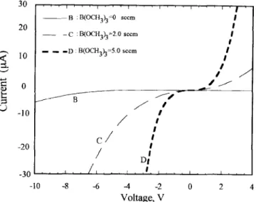
a constant annealing temperature of 900 “C in helium
ambient for 30 min are shown in Fig. 2. After the
annealing treatment, there was no deterioration in the
Z-T/ characteristics of the undoped diamond films. For
the boron-doped diamond film (B(OCH,), =2 seem),
the leakage current for the 10 V forward voltage
increased by a factor of 2 and deterioration in the
rectifying characteristics was observed. Increasing
the B(OCH,)3 flow to 5 seem caused the diamond films
to exhibit more ohmic behavior. We are interested in
the differences in the Z-v characteristics of the boron-
doped diamond films caused by annealing prior to
metallization. We speculated that the annealing would
cause boron atoms doped into the diamond films and
located in inactive sites (e.g. interstitial and clustering
30 20 ^4 lo V 2 g 0 5 -10 -20 -30 ““,“‘,‘,‘,,‘,,“‘,,,’ ~ B : B(OCH3)34 scan I _ -C : E3@CH3)+0 scan r’ _ _ -D B(OCH&=5.0 scan : I 1’ / .lO -8 -6 -1 -2 0 2 4 Voltage, V
Fig. 2. I-V characteristics of Al contacts to “as-deposited” diamond films with various dopant concentrations after 900 “C annealing treatment.
sites) to be incorporated into substitutional sites in the films. The increase in the number of substitutional boron atoms would then change the Z-I/ characteristics of the
boron-doped diamond films because of the tunnelling
effect. This hypothesis was examined in our FTIR and
CL experiments from the viewpoint of bonding behavior, carrier concentration, and CL emission intensity. 3.2. FTIR analysis of diamond films
FTIR experiments were carried out to examine the
difference in the bonding behavior of boron atoms in
the diamond films that resulted from annealing in helium ambient at 900 “C for 30 min.
To more clearly resolve the absorption due to the
incorporation of boron in the lattice of the diamond
films, spectra were taken from samples compressed with
free-standing diamond films and dry KBr powder.
As shown in Fig. 3(a), a broad band was detected in
the region of 3000-3500 cm-’ due to O-H stretching
vibrations of molecular water physisorbed on the surface
of the diamond or diamond-KBr pellets. A peak due to
O-H bending vibrations was also found at 1650 cm- I.
This result suggests that the diamond surface readily
adsorbs atmospheric water on the polar carbonyl groups
[ 141. The weaker band appearing at 2450 cm-’ was
identified as the O=C=O stretching vibrations band.
This means that a small amount of CO, was physically
adsorbed onto the sample surface from the atmosphere.
A sharp peak at 1380 cm-’ and a small peak at around 2980 cm-’ were due to bending and stretching vibration
bonding of C-H, respectively. The peaks at 620, 1180
and 1360 cm- 1 were due to boron present in the boron-
doped diamond films. These well-known bands have
been defined as the O-B-0 vibration [15] and B-H
deformation bands [ 161.
When the diamond films were annealed and then
compressed with KBr powder into transparent pellets,
r
Wavenumber (cm-’ )
Fig. 3. Infrared absorption spectra of pellets formed from diamond films compressed with KBr powder. The doped diamond films were deposited using CO,= 30 seem mixed with CH,= 19.2 seem, B(OCH3)3 = 2 seem (a) as-deposited (b) after annealing.
454 C.-F Chen, S.H. ClwnlDiamond and Related Matrrials 4 i 1995) 451 -455
infrared absorption spectra of the annealed films were
as shown in Fig. 3(b). After annealing, the spectra of the diamond films contained significant bands in the region
of 2800-2980 cm I, which can be ascribed to C-H
stretching vibrations of sp3 hybridized bonding. This
indicates that the annealing caused hydrogen atoms
present in the diamond films to migrate from inactive to active sites and bond with carbon atoms.
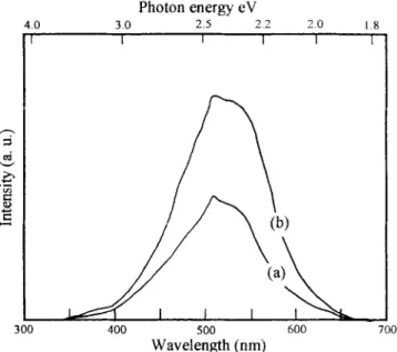
3.3. Carrier concentration measured by CL measurement
Cathodoluminescence spectroscopy were used to
examine the difference between the boron atoms in
annealed and non-annealed diamond films. The CL
spectrum of undoped diamond film shows a main emis-
sion peak at 2.8 eV. For the boron-doped diamond films, the emission peaks were located at 2.352.40 eV and the
intensity was higher than that of undoped diamond
films. The variation of the emission band between
2.0-3.5 eV can be explained directly by the distance
between D-A pairs [ 171. The increase in the CL inten-
sity at 2.4 eV can be explained by the increase of
substitutional boron, which becomes an acceptor in the
D-A pair recombinations. As shown in Fig. 4, the inten- sity of CL at 2.4 eV increased dramatically after annea- ling was performed. From the change in the intensity of CL at 2.4 eV, it appears that the amount of substitutional
boron in the boron-doped diamond films increased
because of the annealing treatment. The number of
substitutional boron atoms increased, resulting in an
increase in the CL intensity at 2.4 eV after annealing.
This result confirmed again that inactive boron atoms
were activated and the I-V characteristics of the boron-
A 0 Photon energy eV 3.0 2.5 22 20 18 I I I I I 400 500 600 700 Wavelength (nm)
Fig. 4. CL spectra of diamond films deposited using CH,!CO,= Fig. 6. Carrier concentration of boron-doped diamond film using 19.2130 seem and B(OCH,), = 2 seem: (a) as-deposited and (b) after CH,;CO,= 19.2!30 seem and B(OCH,),= 2 seem diamond film at
annealing treatment. 900 ‘C with annealing treatment.
doped diamond films were altered by the annealing
treatment.
3.4. Carrier concentration measured by C-I/method
The C-V curves of the Al-diamond contacts were
performed (not shown here) with boron concentration
equal to 3.8% in the gas phase. Assuming the dielectric constant c (=5.7 e,,) is uniform over the entire film, the
depth W from the surface is given by c/C. Inserting
experimental values in the expressions in W and N,, we
can derive the depth profile of the activated boron
concentration beneath the Al electrode. as shown Fig. 5 and Fig. 6. Fig. 5 shows the depth profile of carrier
concentrations in the boron-doped diamond film (B =
3.8%) before the annealing treatment. It is interesting to
compare the mean N, values obtained from the
1o19 I 1 I t
10’6
1
/ 42 44 47 49 52 Depth (elm)Fig. 5. Carrier concentration of boron-doped diamond tilm using CH,!CO, = 19.2;30 seem and B(OCH,), = 2 seem
1
30 31.1 32 3 33.4 34.5
C.-F. Chen, S. H. ChenlDiamond and Related Maierials 4 (1995) 451-455 455
depletion approximation measurement, representing a
selected region about 0.4 pm in depth, with those
obtained previously from SIMS measurement. The
boron concentration derived from the B = 3.8% diamond
films using depletion approximation is 6 x 10¹⁶ cmP3
and that obtained using SIMS measurement is
2.2 x 10²’ cme3. It is apparent that the SIMS measure- ment overestimates the value of the boron concentration by a factor of almost 4. We believe the SIMS measure-
ment detected the quantity of the boron atoms in the
diamond films. These boron atoms perhaps located at
the substitutional, interstitial, or clustering sites in the diamond films. Unlike the SIMS technique, the depletion
approximation technique directly measures the number
of charges in the depletion layer. As a result, it is
reasonable for there to be a difference between these
two values.
Fig. 6 shows the depth profile of the annealed boron-
doped diamond film using the depletion approximation
technique. It is evident that the depth distribution of carriers is uniform in the region of 0.31 pm to 0.345 pm.
The carrier concentration in the annealed boron-doped
diamond film is about 1 x lo’* cmm3, which is almost
two orders of magnitude larger than the value for the
non-annealed diamond film. This large increase in the
amount of carriers probably results from the large
number of acceptors. In the boron-doped diamond films,
boron atoms are the dominant acceptors, and the
number of acceptors increases after annealing.
4. Conclusions
At room temperature, the 1&-I/ characteristics of
boron-doped diamond films using aluminum as contacts
exhibited rectifying behavior. As the boron concen-
tration increased, the forward current decreased, owing
to impurity scattering and rectifying behavior. After the
samples were annealed in a helium ambient of 900 “C
for 30 min, the 1-V characteristics changed: the higher
the boron concentration in the doped diamond films,
the more ohmic behavior they presented. CL measure-
ments confirmed that the intensity at 2.4 eV increased
after the annealing treatment was performed. These data
indicate that more substitutional boron atoms were
obtained as a result of annealing and that annealing
altered the Z-T/ characteristics of the boron-doped
diamond films.
Acknowledgments
The authors are pleased to acknowledge financial
support from the National Science Council of China
under contract number NSC 83-0416-009-014.
References [ll c21 c31 [141 151 [61 [71 C81 c91 Cl01 El11 Cl21 Cl31 [141 [151 Cl61 Cl71
L. Reggiani, S. Bosi, C. Canali, F. Nava and S.F. Kozlov, Solid
State Commun.. 30 (1979) 333.
A.V. Bogdanov, I.M. Vikulin and T.V. Bogdanova, Sou. Phys.
Semicond., 16 ( 1982) 720.
E.A. Konoirova, Yu.A. Kuznetsov, V.F. Sergienko, S.D. Tkachenko, A.V. Spitsn and Yu.Z. Danyushevski, Sou. Phys. Semicond., 17 (1983) 146.
V.K. Bazhenov, I.M. Viokulin and A.G. Goonar, Sov. Phys.
Semicond., 19 (1985) 829.
J. Mort, D. Kuhman, M. Machonkin, F. Jansen, K. Okumura, Y.M. LeGerice and R.J. Nemanich, Appl. Phys. Lett., 55
(1989) 1121.
H. Shiomi, H. Nakahata, T. Imai, Y. Nishibayashi and N. and N. Fujimori, Jpn. J. Appl. Phys., 28 (1989) 758.
K. Okano, H. Naruki, Y. Akiba, T. Kurosu, M. Lida and Y. Hirose, Jpn. J. Appl. Phys., 27 (1988) L173.
S.L. Lee, S.J. Lin, J. Hwang, Appl. Phys. Lett., 63 (1993) 524. F. Fontaine, A. Deneuville, E. Gheeraert, P. Gonon, L. Abello and G. Lucazeau, Diamond Relat. Mater., 3 (1994) 623. C.-F. Chen, S.-H. Chen, T.-M. Hong and T.-C. Wang, Diamond
Relat. Mater., 3 (1994) 632.
C.-F. Chen, S.-H. Chen, T.-M. Hong, H.W. Ko and S.E. Sheu,
Thin Solid Films, 236 (1993) 120.
D.K. Schroder, Semiconductor Material and Device Characterization, John Wiley, 1989, p. 132.
SM. Sze, Semiconductor Devices, Wiley, 1985, p. 33.
T. Ando, M. Ishii, M. Kamo and Y. Sato, J. Chem. Sot. Faraday
Trans., 89 (1993) 1783.
K. Nakamoto, Infrared Spectra of Inorganic and Coordination Compounds, 2nd edn., 1970, p. 323.
L.J. Bellamy, W. Gerrard, M.F. Lappert and R.L. Williams, J. Chem. Sot. (1958) 2412.