Pergamon Copyright 8 1996 Published by Elsevier Science Ltd PII: SOO38-1101(96)00070-6
Printed in Great Britain. All rights reserved 0038-I 101/96 $15.00 + 0.00
LOW FREQUENCY
NOISE CHARACTERISTICS
OF
AlInAs/InGaAs
HETEROJUNCTION
BIPOLAR
TRANSISTORS
SHENG-LYANG JANG’, WAY-MING CHEN’, HAO-HSIUNG LIN’ and CHAO-HSING HUANG’
‘Department of Electronic Engineering, National Taiwan Institute of Technology, 43 Keelung Road, Section 4. Taipei 10772, Taiwan. Republic of China
‘Department of Electrical Engineering. National Taiwan University. Taipei, Taiwan, Republic of China (Received 2 7 March 1996)
Abstract-This paper studies both experimentally and theoretically the low frequency noise of AllnAs/InGaAs HBTs (heterojunction bipolar transistors). Experiments were carried out in the frequency range between IO Hz and 100 kHz and the measured collector voltage noise consists of l/f nosie and generation-recombination noise. The HBTs have finite output resistance; we have developed an experimental technique for noise measurement accounting for the finite output resistance, and present a theoretical I/fnoise model for the HBTs. Good agreement between the theoretical and experimental l/f noises has been achieved, and it is found that at high collector current bias the measured I/fcollector voltage noise is due to the mobility fluctuation of carriers in the quasi-neutral emitter. Copyright 0 1996 Published by Elsevier Science Ltd
1. INTRODUCTION
Low frequency noise can limit the bandwidth and stability of a wide variety of integrated circuits. It can be used as a study tool to evaluate the material property and device characteristics. Although noise has been studied for many decades, recently researchers have paid much more attention to the noise in high-speed compound devices. because the advance of technologies provides better control of material quality and thus consistent experimental results can be produced. Heterojunction bipolar transistors (HBTs) have promising ultra-high-speed digital and microwave, and milimeter-wave analog circuit applications. In terms of microwave appli- cations, low-frequency noise, which usually has l/f noise spectra, is of fundamental importance, because microwave oscillator phase noise characteristics suffer from l/fnoise of the devices[l]. In comparison with GaAs FETs, HBTs benefit not only from high-frequency but also from low-frequency noise performance, i.e. low l/‘noise[2]. The low-frequency noise observed in GaAs FET devices originates from fast trapping states that are associated with isolation by the substrate and surface effects[3]. In contrast, the base region of a BJT is screened by conducting emitter and collector tests from these surface and substate effects resulting in a lower noise. Although there have been a number studies on the low-fre- quency noise of HBTs[l-51, the theoretical discus- sions were phenomenological and were based on the theory developed for homojunction Si material. The discussions were described qualitatively, the exact location of the noise source and the nature of its
relationship with the terminal voltages has not been examined in a quantitative way.
It is well established that both current gain and l/f noise are affected by surface recombination current in the extrinsic base region. which is strongly influenced by the device structure and materials. By including a passivation layer at the extrinsic base region of AlGaAs HBTs, the low-frequency noise has been effectively reduced[ 1,4]. AlGaAs/GaAs HBTs, having relatively high surface recombination velocity, are disadvantageous in comparison with AlInAs/InGaAs HBTs and Si BJT. Therefore the AlInAs/InGaAs HBT has lower low-frequency noise[l], in particular lower l/fnoise. Flicker (l/f, noise is an excess noise found to some extent in all types of transistor and some types of resistor. Flicker noise has various origins: in Si bipolar transistors it is caused mainly by traps associated with contamination and crystal defects at the base-emitter junction; it can also be caused by the mobility fluctuation.
This paper studies the noise performance of electronic AlInAs/InGaAs HBTs fabricated by the MBE system with the goal to explore the measure- ment technique, to develop a theoretical HBT l/f noise model. and to evaluate quantitatively the noise performance of AlInAs/InGaAs HBTs. To discuss the l/f nosie model we should have a clear understanding of carrier transport; based on the thermionic emission process and the current-balanc- ing concept we shall construct the HBT Z-V and l/f noise model. Since AlInAs/InGaAs HBTs have a finite value of output resistance[6], and an experimen- tal measurement technique for extracting noise 1581
1582 Sheng-Lyang Jang et al.
sources is unavailable in literature, we shall discuss a voltage and high output conductance, which is measurement technique similar to that presented by believed to be related to low bandgap. To reduce
Kleinpenning[7]. hot-electron injection, inserting an undoped low-
2. THEORY band-gap spacer layer between the low-band-gap
base and high-band-gap emitter was used. The main
2.1. HBT I-V model principle of this simple method is to utilize the voltage
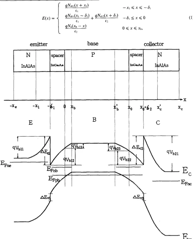
2.1.1. Collector current. A10.481no.szAs/Ino.~,Ga0.47As drop across the undoped spacer layer so as to supress HBT high-speed performance has been demon- the heterojunction spike. Figure 1 shows the energy strated. However, it has been noted by many band diagram of a double HBT with two spacer researchers that InGaAs-collector HBTs typically -* layers. The electric field, E(X), in the suace-charge-re- exhibit low-common-emitter collector breakdown gion (SCR) is given by Ref. [8]. wheie:
E(x) =
c
62emitter
base
collector
SP=
N
JAlAs
(1)
*e
I
IE1583
Fig. 2. Low-frequency, small-signal equivalent circuit of HBT.
where Nd,,, Nd,?. and N, are the doping concen- emitter spacer, and tl, tZ are the permittivities of trations in the emitter, emitter spacer, and base, AlInAs and InCaAs, respectively. From the above respectively. .Y, and xb are the depletion widths in the
emitter and base, respectively. 6, is the width of the
equation we can get xb, xl, and the barrier potentials V,,,, &. Vblz. The potential spike can be evaluated
I L .C
1.1
0.5
0 i-
1584 Sheng-Lyang Jang et al.
I I I
VB,=0.834V
10’ 102 lo3 104 IO5
frequency
(Hz)
Fig. 4. Low-frequency collector voltage spectral intensity versus frequency.
by using AE,,, = AE,, - q(Vb12 + Vb13). The emitter spacer enables band bending in both conduction and valence bands. In the conduction band, it forms a deep notch at the heterointerface. This band bending enables the electron injection energy into the base to be at an optimum, and increases the hole barrier and the current gain. The applied base-emitter (BE) voltage Vk is related to the potential barriers by:
vbk - vbe = vbll + vbl? + vbl3, (2)
where v&c is the BE junction built-in potential and can be derived by using eqn (7).
The electron current density across the BE hetrojunction can be described
thermionic emission fluxes[9,10]:
by two opposed
Jn’(-6,) = -qu.1 [
ne(-6;)
(3)
where vnl = ./zzki, and t)b = .m.
and /?, = mcub/(mb&). q is the electron charge, and V,
is the thermal voltage. m, and mb are the electron masses in the emitter and base respectively. vcr and t)b are the electron thermal velocities in the emitter and base respectively. Assuming the quasi-Fermi levels are flat across the base and emitter SCRs, respectively, then the electron densities in the emitter (n,) and in the base (&) can be written as:
ne(-6;) = n,(-x,)exp (44
(4b)
The electron current density given by eqn (5) is equal to the electron current density due to diffusion, J,i(x& given by:
where the subscript 0 denotes the equilibrium value and &b II” = (8) J,‘(xb) = v,,L”b sinh (n&b) - nbo)cosh UD,k in = 1 + F cosh(g)exp(AE”,qV,). (9) Lb (6) where Ws = xi - .yb, Dnb the base electron diffusion coefficient, and Lnb the base electron diffusion length. The excess electron concentration at the base-side boundary of the BE SCR can be determined by equating (5) and (6):
+
d-x,)
-
exp -qVbe + qVbe + AK,
BI qv,
(7)
Similarly we can derive the Z-V relation in the base-collector (BC) junction. The potential spike is defined as A& = AEc2 - q( vb2? + V&. The applied BC voltage V, can be written as:
Vb,c - Vbe = vb?l + vb?? + vb23, (10)
where Vb,c is the BC junction built-in potential. Similar to eqn (5) the electron current density across the abrupt BC heterojunction can be written as:
JXxo + 62)
= qa& exp(%)(FrM(exp($s - 1)
At
- @b(d) - b0) ,
(11)
1586
Sheng-Lyang Jang et al.
10
-16 c 10 -18 I I Atf=IOHx
0. I 0.2 0.3 0.4 1, (mA) 0.0 0. I 0.2 0.3 0.4 ‘c Cm)Fig, 6. (a) Current-dependence of lilfnosie source at IO Hz. (b) Determination of the dominant measured noise component.
Noise characteristics of AlInAs/InGaAs transistors 1587 where v,,r = ,/qV,/(2 7cm,), /3? = mcvb/(m&. mc is the
collector electron mass. The electron current density given by (11) is equal to the diffusion electron current density, JL(x& given by:
J;(d) =
(ndxb) - nbo) - (nte(x;) - (nw)cosh q&b
-- Lnb
(12)
Substituting (7) into (12), we can get:
Table 1. Device parameters
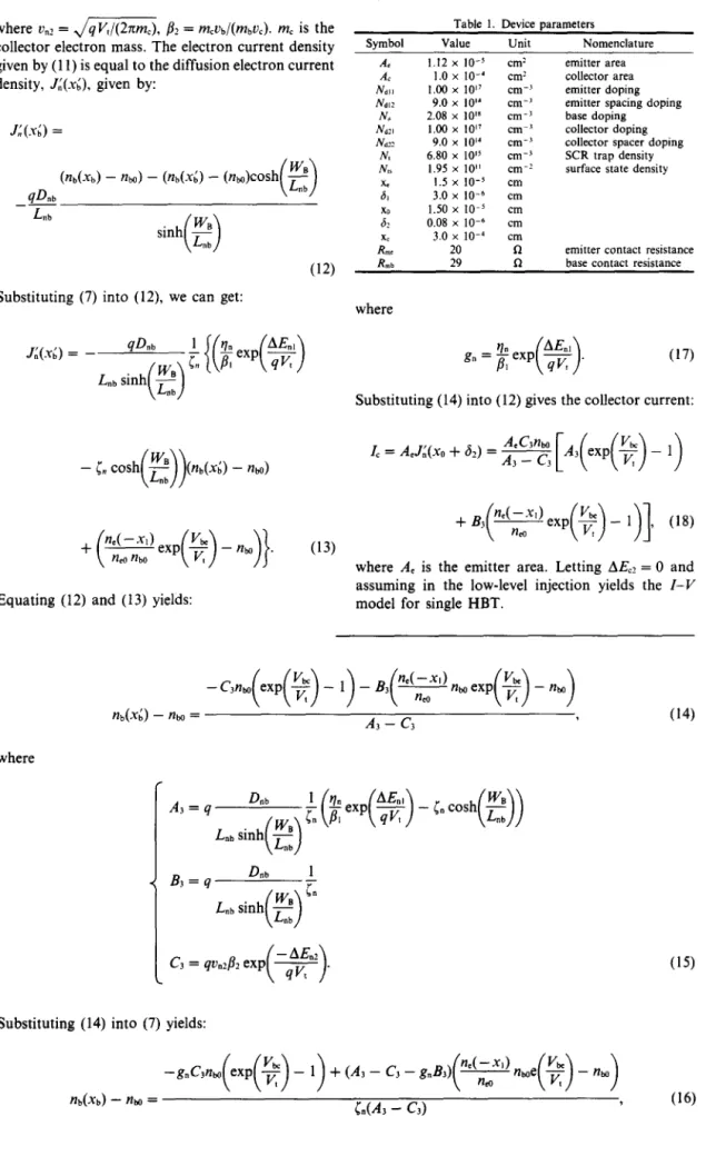
Symbol Value Unit Nomenclature ‘4, 1.12 x IO-’ cm: emitter area A< 1.0 x 10-a cm’ collector area NdII 1.00 x 10” cm-’ emitter doping NdlI 9.0 x IO’” cm-’ emitter spacing doping
N4 2.08 x 10” cm-’ base doping Nd?I 1.00 x IO” cm-’ collector doping Nd,? 9.0 x IO’” cm-’ collector spacer doping
N, 6.80 x 10’5 cm-’ SCR trap density NU 1.95 x 10” cm-’ surface state density
XI 1.5 x 10-I cm 6, 3.0 x 1O-e cm f
P
1.50 x 1O-5 cm 0.08 x lo-” cm xc 3.0 x lo-’ cmRln. 20 R emitter contact resistance Rmb 29 R base contact resistance
where
g”=!bexp
is!
( >
81
9vt
.
(17)Substituting (14) into (12) gives the collector current:
(n&d) - nbo)
+ (*exp(q) - nm)}. (13)
Equating (12) and (13) yields:
I, = A,.qxo + 82) = j+ 3
,
~(ew(+)
- 1)
+ &(y exp(%) - l)], (18)
where A, is the emitter area. Letting AEc2 = 0 and assuming in the low-level injection yields the Z-V model for single HBT.
-C,+exp(%) - 1) -
B,(y
nMexp(!$) - nb0)flb(.&) - flm =
A3 - C3
where
(14)
C3 = qv.& exp .
Substituting (14) into (7) yields:
-g,C3nw(exp($f)-I)+(A3-C3-g”B3)(~nMe($f)-n,)
flbtxb) - flw =
idA3 - C3)
(1%
1588 Sheng-Lyang Jang et al. 2.1.2. Base current. According to the spatial
distribution, there are several base current com- ponents in the HBT including (a) hole current density &(-x,) injected from the base into the emitter; (b) electron-hole recombination current density Jrebrr in the BE SCR; (c) electron-hole recombination current density Jrebr in the BE surface; (d) in the saturation mode holes injected from the base into the collector and contributing to a base current component, &(.uO + 6:). Here we limit the generation-recombina- tion (GR) process to that through Shockley-Read- Hall (SRH) centers.
We first consider (a) the emitter recombination current density. The thermionic hole current density across the BE heterojunction reads:
The excess hole concentration at the emitter side boundary of the BE SCR can now be determined by equating (20) and (22),
PA-‘l)=PCo+;
t&&(-x,)-ppeo) P i+
m(exp(+)
- I)},
(24a) where_ flp,Pb(_“b)e’- 1 bl? cbll- a.% ” “I’), (19)
where llpb = ,/s), rPl = ,,/m, and /I,, = nrpet~pb/(mpb~~pl). nrP, and mPb are the hole masses in the emitter and base respectively. In equilibrium, using (19) we can get the equilibrium emitter hole density, pd. Using (2) and (19) we can get:
(pc( -.Y,) - p&o)
Setting (21) equal to (25) gives
-
n-0(
ew(%)
- l)].
(20)
Pe(-.G) -J&o = $k,(exp(%) - 1) (26a) We assume that at .Y = -.Y, carriers travel at the whererecombination velocity LI,,, hence:
t, = & .q - .u,) = - qc&( - .u,) - p4). (21)
The diffusion current densities in the emitter read:
Kp = 1 - && + &, cos
Substituting (26a) into (24a) yields:
(26b)
and
pet-.Ul)
-pea
. (22)
=i{(qPk+ l)r,,(exp($)- l)]. (27)
Substituting (27) into (19) gives the emitter recombi-
q&c (Pet-.KI)
-pdJ,(_x,) _
P T
nation current density:
where WE = xC - .Y,, D,, the emitter hole diffusion coefficient, and L,, the emitter hole diffusion length.
1589 Secondly we discuss (b) the BE SCR recombination
current density Jrebxr. The SCR recombination current density in the BE SCR can be expressed by -6, J rcbscr = q
s
UwRdx + 9 - I , s -*, Uw&.%
+
s
UsaRdx (29) 0where USHR is the SHR GR rate. The SRH GR process consists of four individual processes: R,, the electron capture rate; Rb, the electron emission rate; &, the hole capture rate; Rd, the hole emission rate. The maximum value of Z&R exists in the BE SCR[ll], we approximate the SCR recombination current density by, for Vk > V,,
z q u VthN,n,,dexp( Vtd2 Vd) - 1) (30)
where W is the thickness of the BE SCR, approximated by (6, + xb). V,,, is the thermal velocity, o is the trap capture cross section, N, is the SCR trap density and nie, is the emitter-spacer intrinsic carrier density.
Thirdly we develop (c) the BE surface recombina- tion current density Jrrbr. The surface recombination current depends on the surface state density, N,,, the characteristics of the surface states and surface charge. In case R,x Rb and &>>&, and in steady-state Uthn% x t’thpbpp. the trap Fermi level is pinned at the trap energy level, then the surface recombination current at the surface of p-n junction perimeter is given by[l2]
I rcbr
a q
WSLS (l),hnb.UlhpQp)“2Nt*(p,n,)“2 (3 1) 2where W, is the length of the perimeter of p-n
junction. n, and pI are the electron and hole densities respectively at the surface. rfhn, &hp, un and up are the electron and hole thermal velocities, and the electron and hole capture cross sections respectively. L, is the effective length for minority carriers confined by the
Coulomb attraction of the surface[l2,13], and:
ng, = nb, exp
( >
mqvbc
.(32)
The net base current is written as:
Ib = AeJ;(-
6,)
+ AcJmbrr
+
kbr + AcJ;(xo + 62) (33) where Ji(xo + 62) is in a similar form as Ji( - 6,). A, is the collector area. The ideality factor of the junction surface recombination current was shown to have a value x 2, whereas the ideality factor is z 1 for the extrinsic base recombination current[ 14,151. 2.2. Physical basis for noise measurementFigure 2 shows the low-frequency, small-signal equivalent circuit of HBTs and its bias circuit, where
Rs, Rc, and RE are respectively the external base,
collector and emitter resistances; rb, r,, and rC are respectively the intrinsic base, collector and emitter resistances; g, is the transconductance, r, is the input base resistance, where g,r, = /3(hFE), p is the current gain. AV;“, is the Nyquist noise for Re, rb, RE. and r,, AVL is the Nyquist noise for RB, rb, Rc, and r,. From the Kirchoff current law we can get:
AZE = Ale + AZ, (34)
AZ -AZ B- eb +B r,
AZc = AZ, + g,,,AV& + % (36)
where rO is the output resistance of the HBT and can be calculated. A represents the fluctuation. Using the Kirchoff voltage law we can get
AKb = -(&I -I- rb)A& - &Arb - (RE + rJAZE - IEAr, + AV;“b (37)
AV, = - (Rc + r,)AZc - IcAr, - (RE + r,)AZE
- ZEArc + AVL (38)
From the above equations we can get:
A& =
-btRALb
+ir- +
Rt)L\z, +
pAV;Nb + ?AVz z_ ((rx + RS)lro)ZcArc + ((r. + Rt)/rO + B)ZEAre + j&A,.,
1590 Sheng-Lyang Jang et al. where
r
/WIFE) = g,r, rl= r, + r0 R5 < = 13Ro Pro - (RE + r,) < RE + re R = RB + rb + RE + re + - gmrO z = [ 1 + RC + r, + RE + r, r01
x (r,
+
R5) + /?(RE + rc). (39b) LFrom the above equation we can arrive at the collector voltage spectral density:
+
(WS, +
(@I
+ p)zE)s, +
(~ZB)~Sra(Z/W
As can be seen, the collector voltage noise is affected by the current noise sources S,, and S,_ the one associated with BC junction is neglected because the BC junction is reverse-biased and the BC current is negligible. It is also affected by the noises (S,, S,,, S,,) generated in the series resistances. The above equations show that S,; is a function of both intrinsic noise sources as well as the equivalent circuit parameters.
2.3. l/f noise origins
Both bulk- and surface-related mechanisms for lif noise have been suggested, we therefore develop the HBT l/f noise model similar to the developed noise model[ 16,171 for homojunction devices.
2.3.1. Model of surface-zlelocity fluctuation l/f
noise. The surface recombination current due to surface state density N,, is:
Zrrbs = q&r Wroti+,N:_tYp,, (41)
where A&= W,L,) is the effective recombination surface area.f; is the occupancy factor. N; is the trap density. We define W, by N,, = N; W,. The total number of charged interface states D,, is defined by: D,, = AcaN,; = A&N,,. (42) We can express the current as a steady-state term plus a fluctuation term, then:
= Irem + quo,,a,(p, - N’;)AD,,, (43)
where we have assumed ApJW, + AN,; = 0. If the statistical event of the deviation AD,, from the average value D,, are independent of each other, then[l6]:
AD,: = [A,nAN’,]’ = A,&1 -f;)N,,.
Combining (43) and (44) yields:
(44)
Following Van der Ziel’s treatment[l6], the spectral intensity of carrier number fluctuation can be defined by: - S,,, = 4AD; s = rg(r)dr OI+o’ (46) where dr g(r)dr = 71n(rl/7d 70 < 7 < 71 otherwise. (47) 0
Since the surface state current is mostly generated by states near the Fermi-level, J; is taken as l/2. If l/to>>cO>>l/r,, from (45) we can get:
(48)
Slm, is the base current spectral density due to the fluctuation current AZrcbn. Using R, = R, and (32) we can get:
(49)
Substituting (49) into (48) we can get SIEb 2.3.2. Model of mobility fluctuation l/f noise. The mobility fluctuation results in the collector current fluctuation AZ,,[16] from which we can get the collector current spectral density, STe given by
1
s,_ = wz, z, !&_%]&& f
( > (50)
where &b is the electron Hooge parameter in the base, f is the frequency. The base current spectral density S,<,,, due to the fluctuation current AZ,b&i = A&-x,)), is:
where mpe is the hole Hooge parameter in the emitter. The net base current spectral density S,, is S,,,, + SI,,.
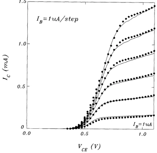
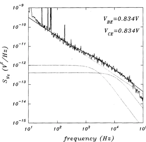
3. EXPERIMENTAL AND THEORETICAL RESULTS This section describes the DC Z-V characteristics and low-frequency noise performance of the InAlAs/ InGaAs SHBTs, which were grown by molecular beam epitaxy[ 181. The output characteristics are shown in Fig. 3. The circled lines are the experimental results, and the solid lines are the fitting results. During the noise measurement, the HBTs were shielded in a metal case to avoid external interference and biased in a common-emitter configuration. The collector was biased in series with a metal-film resistor, the collector voltage is taken out from the collector of the HBT. The collector voltage noises were then fedback to a low-noise amplifier and a PC-controlled spectrum analyzer was used to measure the noise spectrum output from the amplifier. All the experiments were carried out at room temperature. Figure 4 is the collector voltage, spectral intensities at a bias. The noise consists of a l/f noise and G-R noise components.
In Fig. 4, we decompose the noise in terms of its component, and a best fitting for the curve measured at the bias condition of VsE = 0.834 V and
VBc = 0.0 V is as follows:
s,,,y) =
7 +
g’
+
g2
+
cx
(52)
1+&J l+Q
wheref;, andJ1 are the roll-off frequencies of G-R noises, and we found C, = 3.2 x 10⁻⁹, gl = 1.0 x lo-‘?, f;, = 2300 Hz, gz = 4.1 x lo-‘), Jz = 12,000 Hz, and C, = 5.0 x lo-“. Similarly we
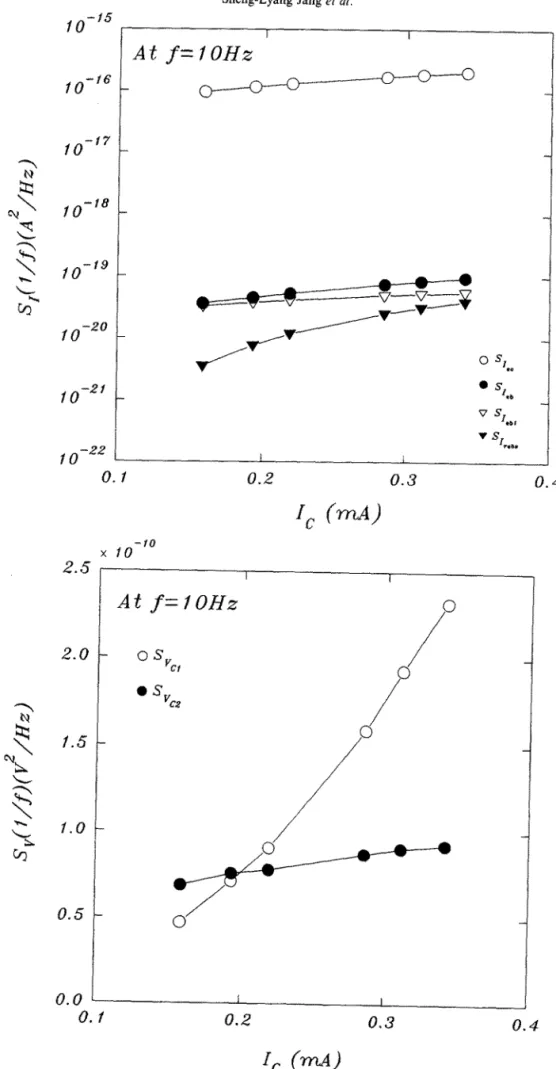
can extract the parameters at other biases. Figure 5 depicts the bias-dependence of the l/fnoise evaluated at
f =
10 Hz and VBc = 0.0 V. The unfilled circle line is the experimental result, and the filled circle line is the fitting result; as seen the trend of the theoretical result is quantitatively the same as the experimental result.To locate the noise source, we plot S,*, (including its components Sr, and S,,,) and S,, versus Z, in Fig. 6(a). We found Sla<<Sl,, the noise source in the quasi-neutral base region is larger, however the base-emitter junction noise S,*, is amplified and the base-collector l/f noise S,_ is not amplified. In Fig. 6(b), we plot Sv,, = (/?@?Rc/Z)?S,c, and Sv,, = (r, + R<)Rc/Z)2S,, of eqn (40) versus the collector current, it is obvious that at high collector current the former term is dominant in the collector voltage noise spectral density, Sv,. The collector voltage noise results from the fluctuation of charged surface states in the emitter-base surface and the mobility fluctuation in the quasi-neutral emitter, and the latter is dominated. At low collector current, the current gain is reduced and the mobility fluctuation in the quasi-neutral base is dominated. This indicates that the bias-dependent circuit
elements play a very important role in determining the measured noise.
In the theoretical calculation the band-edge discontinuities for a heterojunction are given by[20,21] AE, = 0.72AE, and AE, = 0.28AE,. The energy band gap for Alo&roS2As is ES = 1.45 eV and the energy band gap for Ga,,.JnO.S~A~ is Eg = 0.75 eV. The mobility and diffusion constant are as in Ref. [22]: p” = 13800 cm2/(Vs) for InosjGao4,As and D. = 40 cm2/s, D, = 9 cm*/s for AlInAs. The other device parameters used in the device model are listed in Table 1. The fitting Hooge parameters: unb = 1.2 x 1O-5 and zpe = 7 x 10m6, fall into the regime of reported values[ 191.
4. CONCLUSION
It has been shown[2] that the AlInAs/InGaAs HBTs have lower low-frequency noise compared with AlGaAs/GaAs HBTs; the comparison was based on the same measurement technique for AlGaAs/GaAs HBTs. However the AlInAs/InGaAs HBTs have a high output conductance and AlGaAs/GaAs HBTs have a very low output conductance, we can not ignore the effect of the output resistance on the measurement data. This work has developed the measurement technique by including the effect of output resistance in the small-signal equivalent circuit using a thermionic-emission HBT Z-V model and extracted device parameters. It also presents formulas for the l/f noise sources in the HBTs. By combining the l/f noise source model with the small-signal equivalent circuit, we can calculate the l/f collector- voltage noise. Fitting the theoretical l/f noise with the measured l/f noise, a good agreement has been achieved, and we found the noise source for the measured l/f collector voltage noise locates at the quasi-neutral emitter at high collector current bias, and at the quasi-neutral base at low collector current bias.
Acknowledgements-This work was supported by the National Science Council, Taiwan, R.O.C. under Contract NSC 84-2215-EOl l-006. I. 2. 3. 4. 5. 6. 7. 8. REFERENCES
N. Hayama and K. Honjo, IEEE Trans. Elecrron. Devices 39, 2180 (1992).
S. Tanaka, H. Hayama, A. Furukawa, T. Baba, M. Mizuta and H. Honio. Electron. Lert. 1439 (1990). S. C. Jue, D. J. Day, A: Margittai and M. Svilans, I.&W Trans. Electron. Devices 36, 1020 (1989).
D. Costa and J. S. Harris, IEEE Trans. Elecfron. Devices 39, 2383 (1992).
X. N. Zhang, et al. IEEE Trans. Electron. Devices Lett. EDL-5, 277 (1984).
R. J. Malik et al. IEEE Trans. Electron. Devices Lett. EDL-5, 277 (1984).
T. G. M. Kleinpenning, IEEE Trans. Electron. Devices 39, 1501 (1992).
H. R. Chen et al. IEEE Trans. Electron. Device Lett. 15, 336 (1994).
1592 Sheng-Lyang Jang et al. 9. 10. 11. 12. 13. 14.
S. S. Perlman and D. L. Feucht, Solid-St. Electron. 7, 911 (1964).
A. A. Grinberg, M. S. Shur, R. J. Fischer and H. Morkoc. IEEE Trans. Electron. Devices ED-31. 1758 (1984).
S. M. Sze, Physics of Semiconductor Devices. Wiley (1981).
S. Tiwari, Compound Semiconductor Deoice Physics. Academic Press (1992).
C. H. Henry, R. A. Logan and F. R. Merritt, J. Appl. Phys. 49, 3530 (1978).
W. Liu and J. S. Harris, IEEE Trans. Electron. Devices 39, 2726 (1992).
15. 16. 17. 18.
19. M. Tacano, Solid-St. Electron. 34, 917 (1991). 20. D. F. Welch et al. J. Appl. Phys. 3176 (1984). 21. R. People et al. Appl. Phys. Lett. 118 (1983). 22. J. J. Liou et al. Solid-St. Electron. 36, 819 (1993).
W. Liu and S.-K. Fan, IEEE Trans. Electron. Devices Lett. 13, 510 (1992).
A. van der Ziel. Noise in Solid State Deoices and Circuifs. John Wilev. New York (1986).
N. Siabi-Shahrivar-et al. Solid-it. Elktron. 38, 389 (1995).
Chao-Hsing Huang and Hao-Hsiung Lin, Solid-St. Electron. 36, 1229 (1993).