國立交通大學
電子工程學系 電子研究所碩士班
碩 士 論 文
精確且高效率之
蕭基位障萃取程序
An Accurate and Efficient Procedure for
Schottky Barrier Height Extraction
研究生:傅子瑜
指導教授:崔秉鉞 教授
精確且高效率之蕭基位障萃取程序
An Accurate and Efficient Procedure for Schottky
Barrier Height Extraction
研究生:傅子瑜 Student : Tz-Yu Fu
指導教授:崔秉鉞 Advisor : Bing-Yue Tsui
國立交通大學 電子工程學系 電子研究所
碩士論文
A thesis
Submitted to Department of Electronics Engineering and Institute of Electronics College of Electrical Engineering and Computer Engineering
National Chiao Tung University In Partial Fulfillment of the Requirement
for the Degree of Master of Science
in
Electronics Engineering
2012
Hsinchu, Taiwan, Republic of China
i
精確且高效率之蕭基位障萃取程序
研究生: 傅子瑜 指導教授: 崔秉鉞
國立交通大學
電子工程學系 電子研究所碩士班
摘要
隨著半導體製程微縮,半導體元件的接觸電阻也因為面積縮小而增大,而晶 片迴路的總驅動電流也因此被降低。為了繼續微縮元件,如何有效降低接觸電阻 變成是一個重要議題。而接觸電阻與蕭基位障、基板濃度等因素息息相關,因此 可藉由調整此兩種參數去降低接觸電阻。許多研究指出經由特定製程可有效降低 蕭基位障,例如:離子佈植、熱退火處理,並給出等效的蕭基位障值。然而這些 蕭基位障都是藉由熱游離模型萃取而得,而只採用熱游離模型的傳導機制對於萃 取蕭基位障並不足夠。經過特定製程之元件,其半導體表面電場可能已被大幅提 升,電流傳導機制也可能不再是熱游離模型主導。因應高電場效應,場發射模型 應被考慮在傳導機制中。藉由萃取正確的蕭基位障,經由特定製程所導致之實際 影響才能被正確討論及應用。 本研究建立一完整考慮熱游離、場發射、鏡像電荷導致位障降低及寄生電阻 等機制的蕭基位障擷取程序。經以技術電腦輔助設計軟體模擬,驗證此程序之正 確性。不同位障高度、不同基板濃度以及非均勻摻雜之基板也在模擬作業中被完 整討論。更進一步地研究各種材料之基板所形成的蕭基接面,以及不同離子佈植 條件之影響,最後再探討本程序對於萃取極低蕭基位障之可行性。 在模擬作業中,模擬工具與實際之鏡像電荷導致位障降低機制之差異已被完 整討論。由於模擬工具中的鏡像電荷導致位帳降低機制模型過度簡化,導致模擬 結果不能完全符合實際之蕭基接面。在不同基板濃度之模擬中,討論了電流密度 隨逆偏電壓之變化。由於高濃度基板造成更嚴重的鏡像電荷導致位帳降低之影響,ii 對數軸中電流密度對電壓之斜率會隨著濃度提升。在非均勻摻雜之基板模擬中, 討論了表面濃度提升之影響。表面濃度提升並不會降低蕭基位障,而只是造成更 嚴重的鏡像電荷導致位障降低之影響。 在實驗中驗證了此萃取程序對於不同基板材料,例如:碳化矽、鍺、矽,之 可行性。另外,碳離子佈植對矽化鎳/矽接觸面之蕭基位障高度的影響也在此被 討論。從程序中萃取之蕭基位障及載子濃度得知,碳離子佈植對蕭基位障並無作 用,僅僅只是提升等效載子濃度。再來藉由矽化鉑/矽接觸面之蕭基接面探討此 程序對於極低蕭基位障萃取之可行性。蕭基位障隨溫度變化之現象在低溫測量被 觀測到,而其可能是由於半導體表面能階改變導致費米能階鎖定位置不同。最後 研究了氟化硼離子佈植對蕭基接面之影響。跟模擬結果作比較後,我們相信硼離 子會加強鏡像電荷導致位障降低之效果,而氟離子會有修補表面能階之功能。 本研究提出了一項快速且準確的蕭基位障擷取程序。擷取過程僅需數十秒, 且量測得到的數據不需要額外的人工處理。因此,特定製程對蕭基接面之影響可 以被正確地探討及應用。
iii
An Accurate and Efficient Procedure for
Schottky Barrier Height Extraction
Student: Tz-Yu Fu Advisor: Bing-Yue Tsui
Department of Electronics Engineering
Institute of Electronics
National Chiao Tung University
Abstract
As the scaling of the semiconductor fabrication process, the contact resistance in semiconductor devices becomes larger due to the smaller contact area, and the total driving current is degraded. How to reduce the contact resistance is an urgent issue for the continued scaling. Contact resistance is highly dependent on the Schottky barrier height (SBH) and the substrate doping concentration, so they can be lowered by adjusting these two parameters. Several studies have been proposed that the SBH can be lowered by some specific fabrication processes, for example ion implantations and thermal annealing, and those literatures reported the effective SBHs. However, these SBHs are extracted by the thermionic emission (TE) model, and it is not adequate for extracting the actual SBH. For the devices after specific fabrication process, the electric field near the semiconductor surface may be intensively increased, and the conducting mechanism may be no longer dominated by the TE model. For the high electrical field, the field emission (FE) model should be considered into the conducting mechanism. Without extracting the actual SBH, the effect of the specific fabrication process cannot be correctly discussed and applied.
iv
In this thesis, we setup a procedure to extract the SBH considering thermionic emission, field emission, image-force barrier lowering (IFBL) model and parasitic resistance thoroughly. The validity of the proposed procedure is verified and confirmed by technology CAD tool. Different SBHs and different substrate doping profiles have been discussed in the simulation work. Furthermore, the Schottky junctions on different semiconductor materials and the effects of ion implantations are studied, and the validity of extracting the exact low SBHs is discussed at last.
In the simulation work, the difference of the IFBL models between the real case and the simulating tool is explored. The IFBL model in the simulation tool is too simple to fit the real Schottky junction. In the simulation of different substrate doping concentrations, the current-voltage characteristics at reverse bias are discussed. The slope in the log(J)-V raises as the concentration increases due to the severe IFBL effect. In the simulation of non-uniformly doped profiles, it is observed that the increasing of the surface doping concentration does not lower the actual SBH but induce severe IFBL effect.
In the experiment, the validity of extracting the SBHs on various semiconductor materials including silicon carbide, germanium, and silicon, by the proposed procedure is verified. Furthermore, the effect of carbon ion implantation on the SBH of NiSi/Si contact is discussed. The extracted SBH and doping concentration show that the carbon ion implantation does not change the SBH but simply increases the effective carrier concentration. The validity of the exact low barrier height extraction is verified through the case of PtSi/Si Schottky junction. The temperature dependence of the SBH is observed at low temperature, and it is believed that the make-up of the surface states is changed and results in Fermi-level pinning at different energy levels. Finally, the effect of BF2+ ion implantation on the Schottky junction is discussed. In
v
enhance the IFBL effect and the fluorine ions have the ability to repair the surface states.
This thesis proposes an efficiency and accurate procedure for the SBH extraction. It only takes about tens of seconds, and it is not necessary to cope with the measured data artificially. The effect of the specific fabrication process on the Schottky junctions can be correctly discussed and applied.
vi
致謝
此篇論文承蒙許多人的幫助才得以完成,過程中遇到許多挫折與困難也讓我 成長、學習許多。謹以此文來感激這兩年內幫助我的人們。 首先,感謝我的指導教授 崔秉鉞老師。從大學做專題時期就開始指導我如 何正確地做研究、有效率地分析數據與討論,在老師的悉心指導下讓我成長許多, 不只是做研究,也學習到如何能更圓融地去待人處事。 感謝實驗室的大家,振銘、嶸健、元宏、培宇學長無論是在訓練機台、實驗 討論都給予我相當大的幫助。另外感謝高銘鴻同學,從大學做專題時就是一直陪 我討論的夥伴,研究上很多不了解的東西都是在跟他的討論過程中慢慢摸熟。此 外,定業學長也在我車禍期間幫我準備上課筆記讓我修課順利完成。同屆同學克 勤、茂元、孫銘鴻也在我腳行動不便時,在實驗上幫助了我許多。另外感謝罩哥 王培宇,在兩年枯燥乏味的實驗生活中,他的幽默風趣帶給實驗室許多歡笑,崇 德、哲儒、雪君、翰奇、泰源與國丞也讓我的實驗生活添增許多樂趣。 再來感謝我的女朋友炫滋,總是適時地幫我分擔壓力與鼓勵,讓我能有動力 再往下一步邁進。最後感謝我的父母,在車禍期間的照顧與鼓勵讓我不意志消沉, 更讓我能無後顧之憂地進行研究,謝謝你們。vii
Contents
Abstract (Chinese) i
Abstract (English) iii
Acknowledgements vi
List of Tables ix
List of Figures xi
Chapter 1 Introduction………1
1-1 Fundamental Properties of Schottky Barrier……….1
1-1.1 Schottky barrier………1
1-1.2 Fermi-level Pinning………..3
1-1.3 Barrier Lowering………..3
1-2 Potential Application of Low Schottky Barrier………..4
1-3 Conducting Mechanism in the Schottky Barrier……….5
1-4 Traditional Extraction Method of the Schottky Barrier………...6
1-4.1 Current-Voltage Method………..6
1-4.2 Capacitance-Voltage Method………..7
1-4.3 Photoelectric Method………..8
1-4.4 Activation Energy Method………..8
1-5 Motivation………9
1-6 Organization………..10
Chapter 2 Extraction Model and Experiments………17
2-1 Extraction Model………..17
2-2 Simulation Settings………..20
2-3 Experiment Settings……….21
viii
2-5 Low temperature measurement……….………..24
Chapter 3 Simulation Results and Discussion……….35
3-1 Schottky Barriers with Constant Doping Profile………..35
3-1.1 Difference between Simulation and Extraction Model………36
3-1.2 The Temperature Limits of Extraction Models………37
3-1.3 Effects of the Doping Concentrations………..38
3-2 Schottky Barriers with Gaussian Doped Profile………...39
3-2.1 Effects of the Peak Concentration………39
3-2.2 Effects of the Junction Depth………...41
3-3 Summary………..42
Chapter 4 Experiment Results and Discussion………53
4-1 Medium and High Height Extractions……….53
4-1.1 Metal/n-SiC Schottky Junctions………..53
4-1.2 Effect of Carbon Ion Implantation………...54
4-2 Low Barrier Height Extractions………...56
4-2 .1 Study of NiGe/n-Ge Schottky Junction………56
4-2 .2 PtSi/ and NiSi/p-Si Schottky Junction……….57
4-2 .3 Effect of BF2+ Ion Implantation………..58
4-3 Temperature Dependence………59
4-4 Summary………..60
Chapter 5 Conclusions and Future Works………..73
5-1 Conclusions………..73
5-2 Future Works………75
References………77
ix
List of Tables
Chapter 3
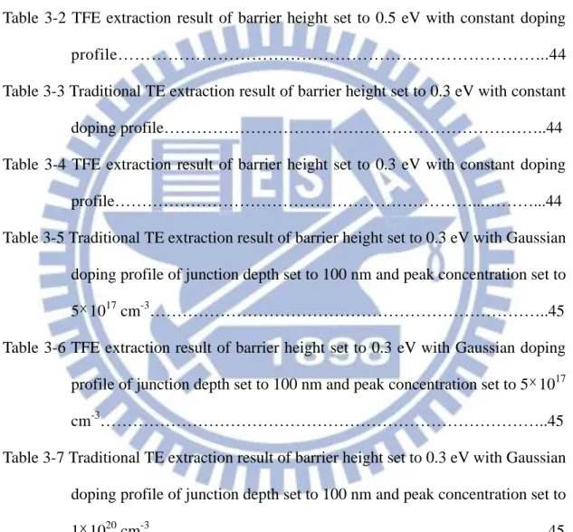
Table 3-1 Traditional TE extraction result of barrier height set to 0.5 eV with constant doping profile………..44 Table 3-2 TFE extraction result of barrier height set to 0.5 eV with constant doping
profile………...44 Table 3-3 Traditional TE extraction result of barrier height set to 0.3 eV with constant doping profile………..44 Table 3-4 TFE extraction result of barrier height set to 0.3 eV with constant doping
profile………...………...44 Table 3-5 Traditional TE extraction result of barrier height set to 0.3 eV with Gaussian
doping profile of junction depth set to 100 nm and peak concentration set to
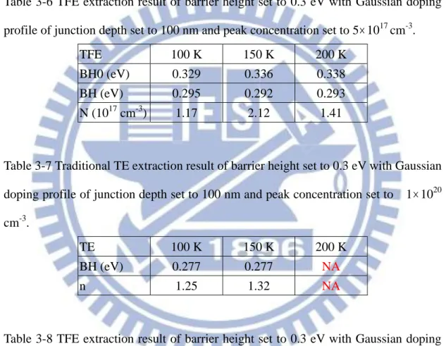
51017 cm-3………..45
Table 3-6 TFE extraction result of barrier height set to 0.3 eV with Gaussian doping profile of junction depth set to 100 nm and peak concentration set to 51017
cm-3………..45
Table 3-7 Traditional TE extraction result of barrier height set to 0.3 eV with Gaussian doping profile of junction depth set to 100 nm and peak concentration set to
11020 cm-3…...………...45
Table 3-8 TFE extraction result of barrier height set to 0.3 eV with Gaussian doping profile of junction depth set to 100 nm and peak concentration set to 11020
cm-3………..45
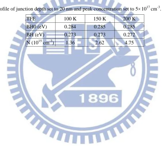
Table 3-9 Traditional TE extraction result of barrier height set to 0.3 eV with Gaussian doping profile of junction depth set to 20 nm and peak concentration set to
x
51017 cm-3………46
Table 3-10 TFE extraction result of barrier height set to 0.3 eV with Gaussian doping profile of junction depth set to 20 nm and peak concentration set to 51017
cm-3………..46
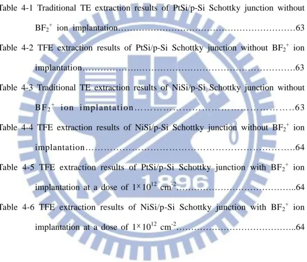
Chapter 4
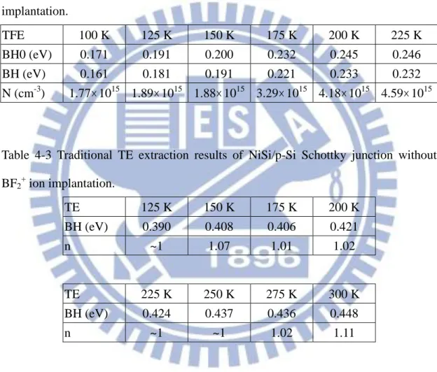
Table 4-1 Traditional TE extraction results of PtSi/p-Si Schottky junction without
BF2+ ion implantation………63
Table 4-2 TFE extraction results of PtSi/p-Si Schottky junction without BF2+ ion
implantation……….……….63 Table 4-3 Traditional TE extraction results of NiSi/p-Si Schottky junction without BF2+ i on i mpl a nt a t i on ……… ………… ………… ………… … . .6 3
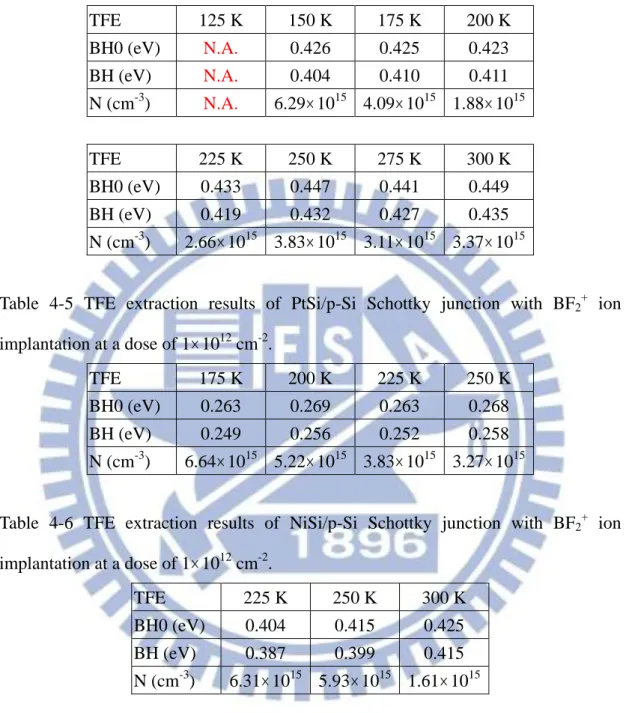
Table 4-4 TFE extraction results of NiSi/p-Si Schottky junction without BF2+ ion
implantation………..64 Table 4-5 TFE extraction results of PtSi/p-Si Schottky junction with BF2+ ion
implantation at a dose of 11012 cm-2………..64 Table 4-6 TFE extraction results of NiSi/p-Si Schottky junction with BF2+ ion
xi
List of Figures
Chapter 1
Fig.1-1 Process of the Schottky barrier formation. (a) Neutral materials separated from each other and (b) electrical equilibrium situation after the contact has been made………...12 Fig.1-2 Schematic diagram of Fermi-level pinning effect. Electron energy band
diagrams of n-type semiconductor with surface states………..12 Fig.1-3 Image force barrier lowering effect. The actual Schottky barrier height lowers
down due to the image potential energy………...….13 Fig.1-4 Conducting mechanisms of the Schottky barrier. (1) is the TE mechanism, (2)
is the FE mechanism, (3) is the recombination process in the space-charge region and (4) is the hole injection from the metal to the semiconductor………13 Fig.1-5 Example of current-voltage method. Forward current density versus applied
voltage, and the barrier height could be extracted from the intercept value..14 Fig.1-6 Example of capacitance-voltage method. The barrier height could be extracted
from the intercept at the voltage axis……….14 Fig.1-7 Setting of the photoelectric method. The electron in the metal is excited by
heat and penetrates the barrier………...……15 Fig.1-8 Example of photoelectric method. The measured data with low photon energy
is interfered with the carrier excited by heat, so the barrier height is extracted by the data with high photon energy………..15 Fig.1-9 Example of activation energy method. The barrier height could be extracted
xii Chapter 2
Fig.2-1 Thermionic-field emission schematic diagram. Holes in the metal are thermally activated and penetrating the Schottky barrier………...26 Fig.2-2 Extraction flow of TFE method. This procedure is realized by the math
tool MATLAB………27 Fig.2-3 Gaussian doped profiles of the simulation. (a) The peak concentration is set to 51017 cm-3, and the depth of the profile is set to 20 nm (b) The peak concentration is set to 51017 cm-3, and the depth of the profile is set to 100 nm………..28 Fig.2-4 Energy band diagrams of the simulation. (a) Constant doping profile, the
substrate doping concentration is set to 31015 cm-3 (b) Gaussian doped profile, the substrate doping concentration is set to 31015 cm-3, peak concentration is 51017 cm-3, and the depth is 100 nm (c) Gaussian doped profile, the substrate doping concentration is set to 31015 cm-3, peak concentration is 11020 cm-3, and the depth is 100 nm (d) Gaussian doped profile, and the substrate doping concentration is set to 31015 cm-3, peak concentration is 51017 cm-3, and the depth is 20 nm (e) Gaussian doped profile, and the substrate doping concentration is set to 31015 cm-3, peak concentration is 11020 cm-3, and the depth is 20 nm...31 Fig.2-5 Device configuration of Metal/SiC Schottky junction………32 Fig.2-6 Device configuration of Metal/Si Schottky junction with carbon ion
implantation………...………32 Fig.2-7 Device configuration of Metal/Ge Schottky junction………..33 Fig.2-8 Device configurations of Metal/p-Si Schottky junction with BF2 ion implantation (a) PtSi/p-Si (b) NiSi/p-Si…...………..………34 Fig.2-9 The chamber of the probe station Lake Shore CPX-VF…………..…………34
xiii Chapter 3
Fig.3-1 Electrical characteristics are simulated by Sentaurus with constant doping profile and metal work function set to 4.55 eV. Temperature ranges from 100 to 300 K………..47 Fig.3-2 Characteristics difference at the temperature of 300 K between the TFE model
and the TCAD tool. The SBH is set to 0.5 eV, and the doping concentration
is set to 3x1015 cm-3………47
Fig.3-3 Electrical characteristics are simulated by Sentaurus with constant doping profile and metal work function set to 4.35 eV. Temperature ranges from 100 to 300 K………..48 Fig.3-4 Extracted SBHs with TE model and TFE model for uniformly doped cases..48 Fig.3-5 Electrical characteristics are simulated by MATLAB with TFE model. The
barrier height is set to 0.3 eV and the temperature is set to 100 K. Doping concentration ranges from 11015 to 11017 cm-3………...……….49 Fig.3-6 Electrical characteristics are simulated by Sentaurus with Gaussian doping
profile and metal work function set to 4.35 eV. The junction depth of Gaussian profile is set to 100 nm and the peak concentration is set to 51017 cm-3. Temperature ranges from 100 to 200 K……...……….49 Fig.3-7 Electrical characteristics are simulated by Sentaurus with Gaussian doping
profile and metal work function set to 4.35 eV. The junction depth of Gaussian profile is set to 100 nm and the peak concentration is set to 11020 cm-3. Temperature ranges from 100 to 200 K…...……….50 Fig.3-8 Extracted SBHs with TE model and TFE model for Gaussian doped case. The
junction depth is set to 100 nm and the peak concentration is set to 51017
cm-3………50
xiv
junction depth is set to 100 nm and the peak concentration is set to 11020
cm-3……….51
Fig.3-10 Electrical characteristics are simulated by Sentaurus with Gaussian doping profile and metal work function set to 4.35 eV. The junction depth of Gaussian profile is set to 20 nm and the peak concentration is set to 51017 cm-3. Temperature ranges from 100 to 200 K…...……….51 Fig.3-11 Electrical characteristics are simulated by Sentaurus with Gaussian doping
profile and metal work function set to 4.35 eV. The junction depth of Gaussian profile is set to 20 nm and the peak concentration is set to 11020 cm-3. Temperature ranges from 100 to 200 K………....52 Fig.3-12 Extracted SBHs with TE model and TFE model for Gaussian doped case.
The junction depth is set to 20 nm and the peak concentration is set to 51017
xv Chapter 4
Fig.4-1 Electrical characteristics of Ni/n-SiC Schottky junction are measured at temperature of 423 and 448 K, including the extraction results by both TE and TFE model………...65 Fig.4-2 Electrical characteristics of Ti/n-SiC Schottky junction are measured at temperature of 300 K, including the extraction results by both TE and TFE model………..65 Fig.4-3 Electrical characteristics of NiSi/n-Si Schottky junction with carbon ion implantation are measured at temperature of 300, 325, and 325 K, including the extraction results by both TE and TFE model………...…………..66 Fig.4-4 SIMS measurement before silicide formation shows the high concentration of
carbon ion near the Schottky junction. SRP measurement shows that the carrier concentration near the junction is only about 1018 cm-3……….66 Fig.4-5 Electrical characteristics of NiGe/n-Ge Schottky junction are measured at
temperature of 300 K, including the extraction results by both TE and TFE model………..67 Fig.4-6 Electrical characteristics of PtSi/p-Si Schottky junction without ion
implantation are measured at the temperature from 100 to 225 K…...…….67 Fig.4-7 Electrical characteristics of NiSi/p-Si Schottky junction without ion
implantation are measured at the temperature from 125 to 300 K……...….68 Fig.4-8 Electrical characteristics of PtSi/p-Si Schottky junction with BF2+ ion
implantation at a dose of 11012 cm-2 are measured at the temperature from 100 to 225 K………..68 Fig.4-9 Electrical characteristics of NiSi/p-Si Schottky junction with BF2+ ion
implantation at a dose of 11012 cm-2 are measured at the temperature from 100 to 300 K………..69
xvi
Fig.4-10 Electrical characteristics of Metal/p-Si Schottky junction with BF2+ ion implantation at a dose of 61012 cm-2 are measured at the temperature from 100 to 300 K (a) PtSi/p-Si: implantation is at a dose 61012 cm-2 (b) NiSi/p-Si: implantation is at a dose 61012 cm-2 (c) PtSi/p-Si: implantation is at a dose 31013 cm-2 (d) NiSi/p-Si: implantation is at a dose 31013 cm-2..71 Fig.4-11 The temperature dependence of the BH0 without considering the IFBL
Effect………..71 Fig.4-12 Illustration of the Fermi energy level and the donor-like interface state
density before metal contact………..72 Fig.4-13 Illustration of the charge distribution in the Schottky junction………72
1
Chapter 1
Introduction
1-1 Fundamental Properties of Schottky Barrier
1-1.1
Schottky Barrier
In 1874, F. Braun has reported the rectifying nature of metallic contacts on iron, copper, and lead sulfide crystal [1]. This is the origin of the metal-semiconductor junction but still far from complete, because their performance is perhaps highly process dependent. But in early 1920s it had been subsequently replaced by vacuum diode. Until the Second World War the point contact diode again became important because of the demand of high frequency converter and low-level microwave detector diode. All these developments are given in the classic book of Torrey and Whitmer [2]. But the contact proved highly unreliable then, it has much superior characteristics nowadays. The significant study toward understanding the rectifying action of metal-semiconductor contact was realized by Schottky and others [3]. Schottky and Mott then explained the mechanism of barrier formation and proposed models for calculating the SBH and the shape of barrier. Till the Second World War, the current transport over the barrier named thermionic emission has been proposed by Bethe [4].
When a metal is contacted with a semiconductor, a potential barrier forms at the metal-semiconductor interface which arises from the separation of charges such that a high-resistance region is created in the semiconductor [5]. The barrier formation process is illustrated in Fig.1. Fig.1-1(a) shows the energy band diagram of an n-type semiconductor with work function qs, which is defined because the Fermi level in the semiconductor varies with the doping concentration, and a metal with work
2
function q
m, which has a volume contribution due to the periodic potential of thecrystal lattice and surface contribution due to the existence of a dipole layer. In n-type semiconductor, q
s is equal to q
q
n , where q is electron affinity of semiconductor and q
n is the difference between semiconductor Fermi level and conduction band edge. What if in p-type semiconductor, qs is equal top
g q
q , where g is the band gap of semiconductor and qp is the difference between semiconductor Fermi level and valence band edge. The energy band diagram in Fig.1-1(a) contains no charge at the surface such that the band structure at the surface is the same as that in the bulk and there is no band bending.
Fig.1-1(b) shows the energy band diagram after the two materials has contacted. After the metal contacted, the Fermi level on two sides must be balanced such that electrical equilibrium can be established: the current flow from the metal to the semiconductor would be equal to the other side at zero bias. Furthermore, the vacuum level at the interface must be continuous, or the electric field would be an infinite value irrationally. Based on these two conditions, the barrier is equal to q(m). The electrons on the semiconductor will flow into metal in this state, so the free electron concentration at the interface surface decreases such that the conduction band bends up as shown in Fig.1-1(b). Thus a positive space charge region is established on the semiconductor side and the electrons flow into the metal form a thin sheet of negative charge. What if in p-type semiconductor, the electrons would be replaced by holes because the major carrier would not be electrons such that a negative charge layer forms at the semiconductor surface, and the electrons at the metal side would be recombined by holes to form a thin positive charge layer.
3
named Schottky barrier which is a main factor to determined current transport at the metal-semiconductor contact.
1-1.2
Fermi-level Pinning
The description above is the ideal case of Schottky barrier, but indeed there is other factor to determine how Schottky barrier forms. Fermi-level pinning is one effect to stand for, and it is a major challenge to decrease SBH nowadays. This phenomenon, which SBH is insensitive to metal work function in covalently bonded semiconductors, was first explained by Bardeen [6] who pointed out that localized surface states would determine the SBH. The surface atom has one broken covalent bond which is also named dangling bond. Dangling bonds would generate energy states at the surface of semiconductor in the forbidden gap. The surface states are usually continuously distributed in the band gap and characterized by a charge neutrality level q0, which is shown in Fig.1-2 [7]. If the SBH is independent of the metal work function, it can be written by qB g q0. Fermi-level pinning effect is mainly caused from metal induced gap states (MIGS) [8-10] and interface dipoles [11, 12], but more details are not concluded here, because this study give more focus on how to measure the SBH.
1-1.3
Barrier Lowering
The other effect which would change SBH is the image force barrier lowering, which is due to the electric field in the depletion region. This effect can be easily understood by Fig.1-3. There is an electric field perpendicular to the metal surface, so an electron must be subjected to the field at a distance x from the surface. The field can be calculated as an image force which is q2 4d(2x)2, so the electron has a
4
negative potential energy q2 16dx which should be added to the barrier energy to obtain the total energy of the electron. The magnitude B of the image force barrier lowering is given by
1/4 2 2 3 8 q N Vi V s d d B [13].Here Nd is the doping concentration of the semiconductor, V is the applied voltage, and d is the image force permittivity which may be different from the static permittivity s. The image force barrier lowering resulted from the field produced by electrons. So when the SBH is measured by a method without movement of the electrons over the barrier, the obtained B will be zero.
1-2 Potential Application of Low Schottky Barrier
As the semiconductor device scales down, contact resistances between metal and source/drain (S/D) become a critical problem due to the scaled contact area. The equation of contact resistance is given as
c c
c A
R , where Rc is the contact
resistance, Ac is the contact area and c is the specific contact resistance which is determined by the contact materials. The equation above shows that the contact resistance would be larger as the contact area becomes smaller. Even though the channel could generate sufficient carriers to raise the theoretical driving capability, the real driving current would be degraded due to the serial resistances at the contacts between metal and S/D, so how to reduce the contact resistance becomes an urgent issue for the aggressive scaling in nowadays.
At the other side, Schottky S/D becomes a possible solution in very large scale integration (VLSI) technology in the future. In order to achieve highly doped junctions, steep lateral profiling and low contact specific resistance, a brand new idea
5
that integrates Schottky S/D in metal-oxide-semiconductor field effect transistor’s (MOSFET) architectures have been proposed [14]. This new idea have inherently solved the problem that control of S/D doping for short gate geometries. Recent publication [15, 16] have shown the need for extremely low Schottky barriers (~0.1 eV) to obtain current drives that compete with highly doped S/D MOSFETs.
Platinum silicide on p-type silicon (PtSi/p-Si) substrate is a good example for low Schottky barrier which has a typical SBH to holes around 0.22-0.25 eV according to the literature [17-20]. The most inviting advantage of PtSi is that specific contact resistance can reach an ultra-low value such that the rectifying effect at the metal-semiconductor junction no longer exists. Specific contact resistance can be
described as D bn c c c N m A R * 2
exp , where R is contact resistance, c
c
A is contact area,
is dielectric constant, and m is the effective mass of the *electron. As the SBH getting lower, the specific contact resistance performs even like an Ohmic contact. So this study focuses on how to extract the SBH of PtSi on p-type silicon substrate by a brand new method
1-3 Conducting Mechanism in the Schottky Barrier
Before starting to introduce the traditional extraction methods of the SBH, it is necessary to understand the current transport of the barrier, because most measurements of the SBH are based on the behavior of the conducting carriers. There are four main conducting mechanisms: (a) thermionic emission (TE) (b) field emission (FE) (c) carrier recombination (d) minority carrier injection. All these four mechanisms are described in Fig.1-4. In general case, (c) and (d) take very small part
6
of the total current, so this study only discusses (a) and (b) for extracting the SBH. TE is the most popular mechanism in extracting the SBH, and it can be written in
* 2exp exp 1 kT qV kT T AA I b ,
where A is the diode area and A* is the Richardson constant which is a variable of
the effective mass of the conducting carrier [21]. The most treatment is completed by Crowell and Sze [22], FE is the other dominant mechanism to make up the insufficiency of TE. When barrier is thin enough, the carrier in semiconductor would pass through the barrier by tunneling through it. This situation can be realized in a highly doped semiconductor material, because higher doping concentration would cause higher electric field in metal-semiconductor contact. This study focuses more on how to combine TE and FE to measure the SBH, because the carrier would not stay at the band edge but thermally excited to a higher level. When a carrier is thermally excited to a higher level, it may see a lower barrier than when it stays at the band edge. Then the carrier would pass through the lower barrier by FE, the two step of the conducting mechanism is known as thermionic field emission (TFE).
1-4 Traditional Extraction Method of the Schottky Barrier
After realizing the main conducting mechanisms, following introduces the extraction methods of the SBH. There are also four main methods: (a) current-voltage method, (b) capacitance-voltage method, (c) photoelectric current method, and (d) activation energy method.
1-4.1
Current-Voltage Method
The current on the Schottky barrier is due to thermionic emission, so the SBH can be extracted by the equation
7 , 1 exp exp 2 * nkT qV kT T A J b
where n is the diode ideality factor, which is caused by the image force barrier lowering mechanism and the other non-ideal factors such as surface defects and interfacial layer. Because the barrier lowering would be varied by the applied voltage, the exact SBH would be different if the applied voltage changed, so we need to take the ideality factor to modify the slope in current-voltage plot. Assuming the measured data are shown in Fig.1-5, we take some points which is in excess of 3kT/q such that exponential term would be large enough and rewrite the equation into
ln . ln * 2 nkT qV e T A J kT b Knowing the Richardson constant A and the temperature, the SBH value can be *
extracted by extrapolating the straight line to V=0 in Fig.1-5.
1-4.2
Capacitance-Voltage Method
This method is based on the capacitance in semiconductor at reverse bias, and the SBH can be extracted by the equation
q kT V V N q C S D bi 2 1 2 .
By the plot of 1/C2 versus VR which is shown in Fig.1-6, the value of Vbi can be
extrapolated, where Vbi is equal to Vx+kT/q. Vx stands for the applied voltage should
be given for flat band in the semiconductor, and kT/q is a correction term for flat band because the band bending would not be zero even the applied voltage is given. Then we know the barrier can be written in the following equation
q kT V Vx o b and , D C o N N n q kT V .
8
where V0 is the energy difference between Fermi-level and band edge. By adding this
term the real SBH can be calculated, where T and NC are known, ND can be calculated
from the slope of the plot. More comprehensive discussion of this method has been given by Goodman [23].
1-4.3
Photoelectric Method
This method is the most accurate and direct method of determining the SBH. As shown in Fig.1-7, by illuminating monochromatic light on the metal, electrons on the metal would be excited to surpass the barrier such that photocurrent would be generated. The photocurrent can be formulated in the following equation
b
2 ,ph B h q
I
where B is a constant, h is Planck’s constant, and is frequency. We can extract the SBH by extrapolating the plot of Iph0.5versus h as shown in Fig.1-8. In this plot
some limitations in this method can be figured out. First, the photo energy could not be larger than the band gap of the semiconductor, or there would be other current by generation current mechanism in the measurement. Second, if the photo energy is not large enough, the measured data would not be linearly proportional to the photo energy, because the electrons in the metal would be thermal excited so we could not distinguish that the current is generated by the photo or the heat of temperature.
1-4.4
Activation Energy Method
This method is based on the current-voltage characteristic, by changing the variable of V. In case A is unknown, the SBH still could be extracted by the *
thermionic emission model. If we fix the applied voltage and draw the plot of ln(J0/T2)
9
T k V q A T J ( Bn ) 1 ln ln * 2 0 The equation above shows that the slope in the plot would contain the information of the SBH. The applied voltage is known, so the SBH still could be calculated.
1-5 Motivation
After introducing the traditional extraction methods of the SBH, the study now focuses on the issue of the low SBH. Because all this four methods have their limitations, the SBH in the low barrier cases could not be extracted. For current-voltage method and activation energy method, the band bending at forward bias in the low barrier cases would be unobvious. That is, the current in measurement would be dominated by parasitic resistance, so there could not be sufficient data to calculate the SBH in the linear region of the plot. For the capacitance-voltage method, the current at reverse bias in the low barrier cases is too large to measure reliable capacitance value. For photoelectric method, the barrier is too low to distinguish the current generated by photon or by heat. According to these problems, it is known that there is still no precise method to extract the SBH in the low barrier cases. Most of the literature proposed recently used the effective SBH to show how low the SBH they have achieved, but the values are not correct indeed [24-28]. Because the measured I-V characteristics are not thermionic emission dominant, using these extraction methods could not obtain the valid information of the SBH.
The exact SBH determines what conducting mechanism dominates the Schottky barrier, but most traditional methods give the effective values meaninglessly. For example, the current density could be raised by adding donors (or acceptors) into the semiconductor, and the tunneling current (FE) would be the dominant mechanism as the barrier gets thinner. However, the traditional method only takes TE model into
10
consideration, and the extracted values would be effectively lowered down. The results give wrong information, and what did happen after the fabrication process would be never known. In order to avoid such situations, this study proposes a new method which contains more conducting mechanisms.
First, since the information of C-V characteristics of the low barrier is not reliable, the information of I-V characteristics is still necessary. Second, the information of I-V characteristics at forward bias is not sufficient, so the information at reverse bias is taken into consideration such that the image force barrier lowering effect would be more obvious. Such method has been proposed [29], and the conducting mechanism of the Schottky barrier at reverse bias is known as TFE model. But there is still one other problem, the conducting mechanism at reverse bias is no longer a simple TE model, so the SBH could not be extracted by a simple formula. The conducting mechanism of the Schottky barrier at reverse bias named TFE model is a too complicated integral to calculate by hand, so program computing is adopted to replace this hard work. By programing a procedure in MATLAB, the measured data could be fit with theoretical data to extract the information of the Schottky barrier.
1-6 Organization
The first chapter is the introduction including the fundamentals of the Schottky barrier, the advantage and the feasibility of the low barrier cases, traditional extraction methods, and then proposing a new method to overcome the problem of the traditional methods. Chapter 2 shows the procedure of this new method, simulation setting, experiment setting, and process flow.
Simulation result is discussed in Chapter 3. First, the feasibility of this new method is verified by the simulation data. However, the simulation tool is not so intact
11
for the real cases, so the procedure has been verified again by the real Schottky barrier contact with silicon, silicon carbide, and germanium substrates in Chapter 4. To achieve the goal of extracting the exact low SBH cases, platinum silicide on p-type silicon substrates is also studied in the same chapter. Finally the feasibility of this new method has been verified again in the exact low barrier cases. The last chapter is the summary and future works of this thesis.
12
Fig.1-1 Process of the Schottky barrier formation. (a) Neutral materials separated from each other and (b) electrical equilibrium situation after the contact has been made [13].
Fig.1-2 Schematic diagram of Fermi-level pinning effect. Electron energy band diagrams of n-type semiconductor with surface states.
13
Fig.1-3 Image force barrier lowering effect. The actual Schottky barrier height lowers down due to the image potential energy [17].
Fig.1-4 Conducting mechanisms of the Schottky barrier. (1) is the TE mechanism, (2) is the FE mechanism, (3) is the recombination process in the space-charge region and (4) is the hole injection from the metal to the semiconductor [17]
14
Fig.1-5 Example of current-voltage method. Forward current density versus applied voltage, and the barrier height could be extracted from the intercept value [17].
Fig.1-6 Example of capacitance-voltage method. The barrier height could be extracted from the intercept at the voltage axis [17].
15
Fig.1-7 Setting of the photoelectric method. The electron in the metal is excited by heat and penetrates the barrier [17].
Fig.1-8 Example of photoelectric method. The measured data with low photon energy is interfered with the carrier excited by heat, so the barrier height is extracted by the data with high photon energy [17].
16
Fig.1-9 Example of activation energy method. The barrier height could be extracted from the slope in this Arrhenius plot [17].
17
Chapter 2
Extraction Model and Experiments
2-1 Extraction Model
The proposed new extraction method is based on the conducting current under reverse bias of the Schottky barrier, so the TFE model which has been introduced in chapter 1 is adopted in this thesis. The carriers would be thermally excited to a higher energy and pass through the lower barrier, which is shown in Fig.2-1. The TFE model derived under the WKB approximation can be expressed as
1 0 00 0 1 exp 1 y d E kT kT E kT E J JR R b b [24]where E =q(b bp-s+V ) is the band bending in the semiconductor,R bp is the Schottky barrier, s is the energy difference between Fermi level and valence band edge, and V is the reverse bias.R The JR0 shown in the following equation stands
for the reverse saturation current of pure thermionic emission.
kT q T A JRO 2 exp bp
The parameter E00 is a property of the semiconductor through its dielectric constant
s
, the effective mass of carriers m , and the doping concentration N . The ratio
00
E
kT would decide whether the dominant mechanism is TE or FE. The FE model dominates the conducting mechanism at reverse bias in the Schottky barrier when
1
00
E
kT , while kT E00 1 TE is the most significant mechanism.
2 / 1 00 4 s m N qh E
18
The function y
responds the transformation of the integration of TE/FE over distance into one over energy [30]. It can be defined by
1/2 1 11/2 1/2 ln 1 yAbove all we have just introduced the conducting mechanism in this extraction method, now we take other factors into consideration. The first one must be considered is the IFBL effect introduced in Chapter 1.
1/4 2 2 3 8 q N Vi V s d d B The second is the parasitic resistance which can be extracted at forward bias, because we have to deduct the voltage drop due to the parasitic resistance from the measurement. For calculating the energy difference between the Fermi level and band edge, we need to take an appropriate model of density of states (DOS) into consideration, so we take the DOS model from Synopsys Sentaurus [26].
2 / 3 2 ) 2 ( 2 ) ( h T k m T N e B C 3/2 2 ) 2 ( 2 ) ( h T k m T N h B V
t l
e e m m mm m m 2 1/3 0 6
h h mm iT hT gT fT eT dT cT bT a m m 2/3 4 3 2 4 3 2 0 1The constants a , b, c , d , e , f , g , h, i , m , l m , t mm , and e mm in h
above equations depend on materials. At last, we realized this extraction method by MATLAB and the total extraction procedure is shown in Fig.2-2.
In this procedure, the I-V-T data we measured or simulated is input to a designated excel file and the data will be retrieved while the program is running. Before running this program, it is necessary to declare the semiconductor material and doping type, the parameters of semiconductors are given. Then we set the calculating
19
ranges of SBH and N. While running this program, the parasitic resistance will be extracted from the I-V-T data at forward bias. The parasitic resistance is extracted by the slope of the linear region in the I-V-T characteristic at high forward bias, and the extracting rule is that the error of the slopes at continual points must be smaller than 1%. Then take advantage of this resistance value to modify the voltage drop at any bias, because the total voltage consists of the voltage drops across the Schottky junction and the parasitic resistance, and only the voltage drop across the Schottky junction should be used to extract the SBH. Afterwards, the program will calculate multiple I-V-T data with the TFE model and the IFBL effect, compare these calculated data with the measured data in the designated excel file, and adjust the SBH and N until the minimum error is obtained.
There are some critical parameter-setting tricks in the extracting procedure to determine the extraction result converged or not. Before running the program, it is necessary to declare the upper and lower bounds of the SBH and N. Improper settings may cause the extracted results incorrect and the results would be at the bound of the settings. In order to prevent this situation, the program has been modified a little bit. The SBH and N are extracted by 4-step: first, the full range is uniformly divided into 10 parts, and the part with the lowest error is found out. This part is then divided into 10 subparts, and the subpart with the lowest error is found out again. The partition procedure repeats 4 times, and each partition would re-allocate the bound ranges of the SBH and N: if the answers are beyond the pre-set bounds, the program will move the bounds to make the answers inside the bound ranges. After four times calculation, the SBH and N have sufficient accuracy. To fit the I-V characteristics from measured one, there is another parameter m* (effective tunneling mass) needed to be determined. The slope of the leakage current in logarithm scale highly depends on the parameter E00, the higher E00 the higher slope. However, the E00 valueis consisted of (N/m*) 0.5,
20
and it means that the extracted N highly depends on the effective mass for the same E00. What if the m* settings is 10 times by the real one, and the extracted N is also 10
times by the exact one, so the m* setting is critical for each case of the different Schottky junctions.
2-2 Simulation Settings
The electrical characteristics of a Schottky junction with different SBHs and doping profiles can be studied by TCAD simulation. In this thesis, Synopsys Sentaurus was used [31]. The thickness of the silicon substrate is fixed at 400m. The square shape contact area has length 100 m at each side. The thickness of the metal is set to 50 nm and the resistivity is set to 15 ohm-cm. These two parameters do not affect the simulated results almost.
The simulation tool does not include the metal induced gap states (MIGS) model, so the metal work function is the only parameters to determine the SBH. The SBH is ideal in this simulation tool, so the SBH in n-type semiconductor is equal to
m
,and the SBH in p-type semiconductor is equal to g m. In order to fix the SBH at different temperature, the n-type semiconductor is adopted in this thesis, because there is a temperature dependent parameter, the band gap of semiconductor, in the ideal formula for p-type semiconductor.
In this thesis the SBH is set to 0.3 and 0.5 eV, and the substrate doping is set to
15
10
3 cm-3. Two kinds of doping profiles are considered, one is constant doping profile and the other is Gaussian doping profile. The constant doping is simply the original substrate doping. For the Gaussian doping profile, two junction depths of 20
21
and 100 nm are used as shown in Fig.2-3. The peak concentrations are set to 51017 cm-3 and 11020 cm-3. The energy band diagram is shown in Fig.2-4.
2-3 Experiment Settings
The experiments are divided into two parts. In part-1, different metal/semiconductor Schottky junctions, including three different semiconductor substrates, silicon, germanium, and silicon carbide, were used to verify the validity of the proposed extraction procedure. In order to verify that the extracted results are consistent with the traditional TE method, some SBHs should be set high enough, so that we can extract the SBH by forward I-V characteristics. First, Ti and Ni Schottky contacts on n-type silicon carbide (SiC) substrate are adopted, because their SBHs are up to 1 eV [32-38]. Second, we discuss the case of NiSi Schottky contact on n-type silicon substrate. The SBH of this contact is about 0.65 eV [39-42]. The effect of carbon doping on the SBH and N are also studied [43-44]. Finally, we discuss the SBH of NiGe/Ge Schottky contact on n-type germanium substrate. Due to the narrow band gap of germanium and the severe Fermi-level pinning effect, the SBH is around 0.5 eV [45-46]. It can be regarded as a transitive case to the low SBH extraction. The SBH extraction by the TE model at room temperature on this contact has been a considerable difficulty.
In part-2, after the verification of the extraction procedure, SBHs of some low barrier height Schottky contacts were extracted by this procedure. In this part, NiSi and PtSi Schottky contacts on p-type silicon substrate are adopted, because the SBHs of these two contacts are too low, about 0.45 eV and 0.25 eV, respectively [47-50], to be extracted by traditional TE method. On the other hand, the NiSi and PtSi samples with BF2+ implantation are also studied. The implantation energy was 30 keV, and the
22
implant doses were 11012, 61012, and 31013 cm-2.
2-4 Device Fabrication
Metal/SiC Schottky contact:
The semiconductor material was n-type SiC substrate with 11-m-thick epi-layer. After standard RCA clean, a 100-nm-thick SiO2 capping layer was deposited by
PECVD to protect the front side surface during the backside contact process. In order to make backside contact ohmic, a 100-nm-thick Ni layer was deposited on backside and annealed at 1000 oC for 15 minutes by furnace. Before forming front side Schottky contact, the capping oxide was removed by BOE solution, and re-deposited 200-nm-thick isolation SiO2 layer by PECVD. Contact holes were patterned by
conventional optical lithography process, but the photoresist was still remained for metal layer lift-off. A 100-nm-thick metal layer, Ti and Ni were both used, was deposited by sputtering system, and a 300-nm-thick Al layer was coated by thermal coater. After metal layer lift-off, Schottky contacts alloy were carried out by furnace at 500 oC for 5 minutes. The final structure is shown in Fig.2-5.
Metal/Si Schottky contact with carbon ion implantation:
The starting material was (100)-oriented phosphorus-doped Si substrate with a nominal resistivity 2.7~4 ohm-cm. After standard RCA clean, a typical local-oxidation-of-silicon (LOCOS) isolation process was performed. Then, a 70-nm-thick screen oxide layer was thermally grown followed by carbon ion implantation at 40 keV to a dose of 11015 cm-2. The projected ion range of C ions is 58.7 nm under the Si substrate surface, which is slightly deeper than the final NiSi/Si interface. In order to repairing the defects caused by the ion implantation, the sample
23
was annealed by a rapid-thermal annealing (RTA) system at 1050 oC for 30 seconds in N2 ambient. Afterwards, the screen oxide layer was removed by diluted-HF. A
25-nm-thick Ni layer and a 5-nm-thick TiN capping layer were deposited in a sputtering system, and the silicide formation was carried out by a RTA system at 500 o
C for 30 seconds. Then, the TiN capping layer and unreacted Ni were selectively etched by a mixture of H2SO4:H2O2=3:1. Finally, a 300-nm-thick Al was deposited on
the wafer backside to form ohmic contact. The final structure is shown in Fig.2-6.
Metal/Ge Schottky contact:
N-type Ge substrate was adopted, and started the device fabrication with several times diluted HF solution clean. Because Ge could be easily oxidized, and GeO2 is
water-soluble, standard RCA clean is not an appropriate clean process. A 200-nm-thick SiO2 layer was deposited by PECVD, and contact holes were patterned
by conventional optical lithography process. After contact holes etching by BOE solution, the photoresist was still retained for metal layer lift-off. In order to form front side Schottky contacts, Ni (15 nm)/TiN (15 nm) layers were deposited by a sputtering system and the metal outside the contact holes was lifted-off. Germanide formation was carried out by a RTA system at 500 oC for 30 seconds, and the residual metal was removed by hot HCl solution. Finally, backside Al layer of 300-nm-thick was deposited by a thermal coater, and the final structure is shown in Fig.2-7.
Metal/Si Schottky contacts with BF2+ ion implantation:
The starting material was heavily-boron-doped Si substrate with 4-m-thick low doping epi-layer. The high doping substrate (1018cm ) is used to lower the parasitic 3
resistance, and the low doping epi-layer (1015cm ) is used for Schottky junction 3
24
1012, and 31013 cm-2, and activated at 1000oC for 10 seconds. Samples without ion implantation were also retained. After standard RCA clean, 200-nm-thick SiO2 layer
was deposited by PECVD, and contact holes were patterned by lithography. Then, contact holes were etched out by BOE solution, but the photoresist was still remained for metal layer lift-off. Metal layer, both Pt (15 nm) and Ni (15 nm)/TiN (15 nm) layers were used, was deposited by a sputtering system, and the metal outside contact holes was lifted-off. Silicide formation, both PtSi and NiSi, was performed by a RTA system at 500 oC for 30 seconds. The unreacted metal was not etched after the silicide formation for both two cases. Finally, backside 20-nm-thick Pt layer was deposited by sputtering system to form good ohmic contact and the final structure is shown in Fig.2-8. The backside metal selection here is critical, because the resistance values of the front side Schottky junctions are very low. Al would not be an appropriate material for backside contact, because its SBH to p-type Si is too high, and the I-V characteristic would be dominant by backside Al contact. Here we selected Pt as the backside metal because of its low SBH to p-type Si.
2-5 Low temperature measurement
To extract the SBH of the above samples, it is necessary to measure the I-V-T characteristics. Most samples could be measured at room temperature, but the PtSi sample and the BF2+ implanted samples could not because the junction resistance is
too low to measure the rectifying effect at room temperature, and the I-V-T characteristic would be dominated by parasitic resistance. Measurement at low temperature is needed such that the rectifying effect would appear.
Measurement was executed in the probe station of model Lake Shore CPX-VF as shown in Fig.2-9, and the I-V-T characteristics were obtained by the semiconductor
25
characterization system of model Keithley 4200-SCS. At first, samples were put into the chamber of the probe station, and then lowered the air pressure to about 10-5 torr to avoid the solidification of moisture and residual gas molecules. Afterwards, the chamber temperature was lowered to 100 K by liquid N2 circulation, and the I-V-T
characteristics were measured at this temperature. Then the chamber temperature was raised by a step of 25 K for each measurement until the rectifying effect disappeared.
26
Fig.2-1 Thermionic-field emission schematic diagram. Holes in the metal are thermally activated and penetrating the Schottky barrier.
27
Fig.2-2 Extraction flow of TFE method. This procedure is realized by the math tool MATLAB.
28 (a) -0.20 -0.15 -0.10 -0.05 0.00 1015 1016 1017 D o p in g c o n c e n tr a ti o n ( cm -3 ) Depth (um) (b) -0.20 -0.15 -0.10 -0.05 0.00 1015 1016 1017 D o p in g c o n c e n tr a ti o n ( cm -3 ) Depth (um)
Fig.2-3 Gaussian doped profiles of the simulation. (a) The peak concentration is set to 51017 cm-3, and the depth of the profile is set to 20 nm (b) The peak concentration is set to 51017 cm-3, and the depth of the profile is set to 100 nm
29 (a) -0.5 -0.4 -0.3 -0.2 -0.1 0.0 0.1 -1.2 -1.0 -0.8 -0.6 -0.4 -0.2 0.0 0.2 0.4 E n e rg y b a n d d ia g ra m ( e V ) Depth (um) (b) -0.5 -0.4 -0.3 -0.2 -0.1 0.0 0.1 -1.2 -1.0 -0.8 -0.6 -0.4 -0.2 0.0 0.2 0.4 E n e rg y b a n d d ia g ra m ( e V ) Depth (um)
30 (c) -0.5 -0.4 -0.3 -0.2 -0.1 0.0 0.1 -1.2 -1.0 -0.8 -0.6 -0.4 -0.2 0.0 0.2 0.4 E n e rg y b a n d d ia g ra m ( e V ) Depth (um) (d) -0.5 -0.4 -0.3 -0.2 -0.1 0.0 0.1 -1.2 -1.0 -0.8 -0.6 -0.4 -0.2 0.0 0.2 0.4 E n e rg y b a n d d ia g ra m ( e V ) Depth (um)
31 (e) -0.5 -0.4 -0.3 -0.2 -0.1 0.0 0.1 -1.2 -1.0 -0.8 -0.6 -0.4 -0.2 0.0 0.2 0.4 E n e rg y b a n d d ia g ra m ( e V ) Depth (um)
Fig.2-4 Energy band diagrams of the simulation. (a) Constant doping profile, the substrate doping concentration is set to 31015 cm-3 (b) Gaussian doped profile, the substrate doping concentration is set to 31015 cm-3, peak concentration is 51017 cm-3, and the depth is 100 nm (c) Gaussian doped profile, the substrate doping concentration is set to 31015 cm-3, peak concentration is 11020 cm-3, and the depth is 100 nm (d) Gaussian doped profile, and the substrate doping concentration is set to 31015 cm-3, peak concentration is 51017 cm-3, and the depth is 20 nm (e) Gaussian doped profile, and the substrate doping concentration is set to 31015 cm-3, peak concentration is 11020 cm-3, and the depth is 20 nm
32
Fig.2-5 Device configuration of Metal/SiC Schottky junction.
Fig.2-6 Device configuration of Metal/Si Schottky junction with carbon ion implantation.
33
Fig.2-7 Device configuration of Metal/Ge Schottky junction.
34
(b)
Fig.2-8 Device configurations of Metal/p-Si Schottky junction with BF2+ ion
implantation (a) PtSi/p-Si (b) NiSi/p-Si
35
Chapter 3
Simulation Results and Discussion
3-1 Schottky Barriers with Constant Doping Profile
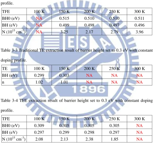
To evaluate if accurate Schottky barrier height (SBH) can be extracted by the proposed extraction procedure, TCAD tool is used to generate the I-V-T characteristics of Schottky junctions with various SBH and substrate doping profiles. Then, the SBH and surface doping concentration (N) are extracted from the simulated I-V-T characteristics using the proposed extraction procedure. At forward bias, the SBH and the ideality factor (n) are extracted by the TE model while at reverse bias; the SBH and N are extracted by the TFE model. At last, comparison between the extracted parameters and the preset parameters in the TCAD simulation are performed.
Fig.3-1 shows the electrical characteristics of the Schottky junction with a metal work function of 4.55 eV. According to the concept of ideal Schottky barrier formation, the SBH here is 0.5 eV. The electrical characteristic at temperature of 100 K is incorrect because the current at reverse bias is too small to be simulated due to the convergence problem of the Schottky-Read-Hall model in the TCAD tool. For the medium SBH, the SBH can be extracted either from the forward biased I-V characteristic using the TE model or from the reverse biased I-V characteristic using the TFE model. The parameters extracted by the TE and TFE models are shown in Table 3-1 and 3-2, respectively. The extracted results from the TE model show that the barrier heights at different temperatures are very close to 0.5 eV, and it means that the TCAD simulation is correct. However, the ideality factor at temperature of 300 K is