國 立 交 通 大 學
資訊工程研究所
碩 士 論 文
應用於無線基頻處理器
之低取樣時間同步迴路設計
Design of Low Sampling based Timing
Synchronization for
Wireless Baseband Application
研究生 : 沈明峰
指導教授 : 許騰尹博士
應用於無線基頻處理器之低取樣時間同步
迴路設計
Design of Low Sampling based Timing
Synchronization for
Wireless Baseband Application
研 究 生:沈明峰 Student : Ming-Feng Shen
指
導教授:許騰尹博士
Advisor : Terng-Yin Hsu
國 立 交 通 大 學
資 訊 工 程 系
碩 士 論 文
A Thesis
Submitted to Department of Computer Science and Information Engineering College of Electrical Engineering and Computer Science
National Chiao Tung University in partial Fulfillment of the Requirements
for the Degree of Master
in
Computer Science and Information Engineering August 2005
Hsinchu, Taiwan, Republic of China
應用於無線基頻處理器之低取樣時間同步
迴路設計
學生:沈明峰 指導教授:許騰尹 博士
國立交通大學資訊工程學系 研究所碩士班
摘要
在現代無線通訊系統中,直接序列展頻(DSSS)和正交頻率多重分割(OFDM)被 廣泛的使用。無線通訊使用空氣當作介質,比有線通訊多了更多的不確定性,因此, 無線通訊系統的封包裡一般都會定義 preamble 欄位作為接收端封包偵測及同步之 用。 而本論文提出一個有效率,應用於 802.11b\g 802.11a\g 自動增益控制、時間同 步演算法。所提出的方法利用安置在每個封包之前的 preamble,在低訊號雜訊比、 載波頻率偏移、多路徑衰減及路徑損失的通道時可以快速,正確的達到前端訊號處 理的完成。而時間同步演算法不同於一般的做法,可以一倍取樣的方式正常工作。 為了瞭解整個系統,我們使用 Matlab 建立了系統模擬平台。我們可以觀察系統中任 一訊號的波形,並且可以得知通道中的非理想效應對整個系統或某些訊號有何影 響。此平台更可以用來驗證我們所提出的演算法,本論文中也放了一些模擬結果圖, 也驗證了演算法的成功。Design of Low Sampling based Timing
Synchronization for
Wireless Baseband Application
Student:
Ming-Feng
Shen
Advisor:
Dr.
Terng-Yin
Hsu
Department of Computer Science and Information Engineering,
National Chiao Tung University
Abstract
Direct Sequence Spreading Spectrum (DSSS) and Orthogonal Frequency Division Multiplexing (OFDM) are widely used in modern wireless communications systems. Unlike the wire channel, wireless communication uses radio as its medium and has more uncertainty with it. Therefore, WLAN frame format generally contains preamble field for packet diction and synchronization.
In this thesis, an efficient automatic gain control (AGC), timing synchronization for DSSS based WLAN defined in IEEE 802.11b\g and 802.11b\a had been proposed. The proposed methods enables a rapid and accurate front-end signal process even under very low SNR, carrier frequency offset multi-path fading and path loss channel by using preamble at the start of every frame. Unlike the general system, the proposed timing synchronization algorithms could work correctly under one times sampling. To get familiar with IEEE standards, simulation platforms were set up with Matlab mathematical software which let us have a chance to probe signals in every place inside the system and visual view of the channel effects. And with this system, our algorithms could be verified. Some simulation results were shown in this thesis and the accomplishment of the proposed algorithms are also verified with these simulation results.
Dedicate the thesis to my family and friends ……
Acknowledgements
I would like to express sincerely my gratitude to those people for their invaluable help during the past two years, stayed in Hsin-Chu. Especially, I want to express my deepest gratitude to my advisor Prof. Terng-Yin Hsu for his enthusiastic guidance and encouragement to overcome many difficulties throughout the research, and I give him and his family my best wish faithfully.
Also, I want to thank my ISIP group mates, You-Hsien Lin(林祐賢), Ming-Fu Sun(孫明福), Jin-Hwa Guo(郭錦華), Ming-Yeh Wu(吳明曄), Light Lin(林弘全), Chueh-An Tsai(蔡爵安), for their suggestions and great helps during my research. I would like to thank all members in ISIP laboratory for their plenty of fruitful assistance.
Finally, I give the greatest respect and love to my family and my girlfriend, Patty. I express my highest appreciation and dedicate the thesis to them for their assistance and attention during the most important stage in my life.
Table of Contents
page
Chapter 1 Introduction………...1
Chapter 2 OFDM/DSSS System and Channel Model ...3
2.1 The basics of OFDM……….….………..3
2.2 The basics of DSSS………....………...4
2.3 IEEE 802.11g PHY Specification……..……....………..4
2.4 Channel Model……....………...…..7
2.4.1 Additive White Gaussian Noise ……….……….….8
2.4.2 Carrier Frequency Offset……..……….……….….8
2.4.3 Multi-path ………..……….……….….8
2.4.4 Sampling Clock Offset ……….……….………….10
2.4.5 Path loss ………..11
C h a p t e r 3 T i m i n g S y n c h r o n i z a t i o n . . … … … . . . … … … 1 3 3.1 System model …..…………....……….………..13
3.2 acquisition algorithm …...……….……….14
3.3.1 1x sampling rate algorithm………....……….……..14
3.3 Tracking algorithm for DSSS/CCK system……….………...17
3.3.1 Tracking algorithm for DSSS..……….……..20
3.3.2 Tracking algorithm for CCK.……….……..22
3.3.3 AGC in DSSS/CCK.……….……..24
3 . 3 . 3 . 1 A G C f o r D S S S . … … … . … … . . 2 4 3 . 3 . 3 . 2 A G C f o r C C K . … … … . … … . . 2 5 3.4 Timing synchronization in OFDM system………....32
Chapter 4 Simulation results………...………37
4.1 Simulation tool……….………..37
4.2 Simulation Results..……….………..38
4.2.2 OFDM part simulation results ……….….………..42
Chapter 5 Proposed Hardware ……….…….………..48
5.1 Matlab to Verilog Design Flow………...…..48
5.2 Design Architecture..……….49
5.3 Proposed hardware component...……….………..50
Chapter 6 Conclusions and Future Works…………...54
6.1 Conclusions ...……….…54
6.2 Future works ...………..………54
List of Figures
page
Figure 2.1 Frame format of ERP-DSSS/CCK…...………..…4
Figure 2.2 Frame format of ERP-OFDM……….5
Figure 2.3 Frame format of DSSS-OFDM………..6
Figure 2.4 Block diagram of transmitter………..…7
Figure 2.5 Block diagram of channel model………....7
Figure 2.6 NLOS and LOS between transmitter and receiver………...9
Figure 2.7 Instantaneous impulse responses………..10
Figure 2.8 Sampling clock may no ideal in the receiver………11
Figure 3.1 state diagram of receiver……...………14
Figure 3.2 sampling location and best sample clock phase………..………15
Figure 3.3 The sample clock phase error after 1X timing acquisition method………….16
Figure 3.4 The MSE versus SNR of 1X timing acquisition method……….16
Figure 3.5 The state diagram of 1X timing acquisition………17
Figure 3.6 correlator powers with perfect channel……….………....18
Figure 3.7 correlator powers with timing drift 100ppm………..………...19
Figure 3.8 correlator powers with timing drift 400ppm………..………19
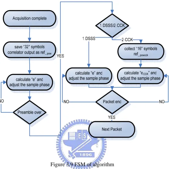
Figure 3.9 FSM of algorithm………..………20
Figure 3.10 correlator output select window………..………..……….22
Figure 3.11 sampling clock phases with tracking algorithm………24
Figure 3.12 AGC control with fine location………..26
Figure 3.13 AGC control with the wrong location………27
Figure 3.14 Coherent with symbol bound………..………28
Figure 3.15 NonCoherent with symbol bound………..…….………28
Figure 3.16 state diagram of AGC……….………29
Figure 3.17 timing synchronization without AGC gain normalization………...30
Figure 3.18 timing synchronization with AGC gain normalization………...30
Figure 3.19 timing synchronization without AGC gain normalization……….31
Figure 3.20 timing synchronization with AGC gain normalization………...31
Figure 3.22 Relation between short preamble and short training sequence…………...33
Figure 3.23 sampling phase diagram………..………...33
Figure 3.24 the sample clock phase error after this timing synchronization method……34
Figure 3.25 the sample clock phase error after this timing synchronization method……35
Figure 3.26 state diagram of timing synchronization………36
Figure 4.1 System block diagram…..……….………...38
Figure 4.2 PER of 2Mbps……….……….39
Figure 4.3 BER of 2Mbps……….……….39
Figure 4.4 PER of 11Mbps………..……….40
Figure 4.5 BER of 11Mbps………...41
Figure 4.6 SCO range that synchronization algorithm can tolerate………...41
Figure 4.7 SCO range that synchronization algorithm can tolerate……..……….42
Figure 4.8 PER of 36Mbps………..……….……….43
Figure 4.9 BER of 36Mbps……….………...43
Figure 4.10 PER of 54Mbps……….……….44
Figure 4.11 BER of 54Mbps……….…..………...45
Figure 4.12 SCO range that synchronization algorithm can tolerate…..………...46
Figure 4.13 SCO range that synchronization algorithm can tolerate……….47
Figure 5.1 Matlab simulation to Hardware implement flow……...………...48
Figure 5.2 the block diagram of dynamic sampling………….……….49
Figure 5.3 the block diagram of DSSS/OFDM/CCK timing synchronization………...50
Figure 5.4 Architecture of timing algorithm for DSSS modulation………..51
Figure 5.5 Architecture of timing algorithm for CCK modulation…………..…………..52
List of Tables
page
CHAPTER 1
INTRODUCTION
With the advance of modern wireless communication techniques, there are more and more wireless communications systems play an increasingly important role in our daily life, like Wireless LAN(IEEE 802.11, 802.11b[1], 802.11a[2], 802.11g[3], UWB). Unlike the wire channel, wireless communication uses radio as its medium and has more uncertainty with it. Therefore, WLAN frame format generally contains preamble field for packet detection and synchronization. In order to understand the timing synchronization problem and solving it, the DSSS system and OFDM system are chosen to be my research area, so the IEEE 802.11g standard is used to build the demo platform to verify the proposed algorithms.
In our thesis, the PLCP preamble is used to do the signal process, such as synchronization and channel estimation which use the Barker spreading code to eliminate non-ideal channel effects including Additive White Gaussian Noise (AWGN), distance path loss, Multipath fading, carrier frequency offset (CFO) and sampling clock offset (SCO). Not only IEEE 802.11g has included a preamble frame, but also many WLAN standards have done that. During this preamble, the signal process, such as timing synchronization, frequency synchronization and channel estimation must be done and some of channel effects have to be eliminated and compensated until the preamble finishes.
Although the preamble formats are not the same in many WLAN standards, the problems that must be solved are all the same. If all these problems on IEEE 802.11g platform are solved, it could quickly find algorithms or solutions that solve these
problems on other wireless platforms. In this thesis, the characteristics of both DSSS /OFDM system and channel models would be described the information of PN spreading code during received preamble.
This thesis includes six chapters; where chapter 1 is the introduction DSSS system. Chapter 2 discusses the channel models and the current used simulation platform, and then chapter 3 discusses the timing synchronization methods in detail. In chapter 4 the performance PER and BER with Matlab simulation platform are shown. Chapter 5 shows the hardware architecture of the proposed system. Finally, chapter 6 is the conclusions and future works for further research.
Chapter 2
OFDM/DSSS System and Channel
Model
In this chapter, we are going to describe tree block of wireless communications, transmitter, channel model, and receiver. At first, we introduce the basic of OFDM and DSSS modulations. And then we present the IEEE 802.11g PHY specification, which combines both 802.11a (OFDM) and 802.11b (DSSS) at one system, and the IEEE 802.11g PHY transmitter block diagram. After that, we characterize some wireless channel models and parameters, such as Additive White Gaussian Noise (AWGN), carrier frequency offset (CFO), multi-path, and so on. Finally, in order to achieve robust synchronizer, we propose a universal receiver system model.
2.1 The basics of OFDM
Orthogonal Frequency Division Multiplexing (OFDM) is a multi-carrier modulation that achieves high data rate and combat multi-path fading in wireless networks. The main concept of OFDM is to divide available channel into several orthogonal sub-channels. All of the sub-channels are transmitted simultaneously, thus achieve a high spectral efficiency. Furthermore, individual data is carried on each sub-carrier, and this is the reason the equalizer can be implemented with low complexity in frequency domain.
2.2 The basics of DSSS
Direct Sequence Spread Spectrum (DSSS) is a spectrum technique whereby the data signals are modulated with spreading code. The principle of Direct Sequence is to spread a signal on a larger frequency band by multiplexing it with a signature or code to minimize localized interference and background noise. To spread the signal, each bit is modulated by a code. In the receiver, the original signal is recovered by receiving the whole spread channel and demodulating with the same code used by the transmitter. A fundamental issue in spread-spectrum systems is how much protection spreading can provide against interfering signals with finite power. Spread-spectrum techniques distribute a relatively low-dimension signal in a large dimensional signal.
2.3 IEEE 802.11g PHY specification
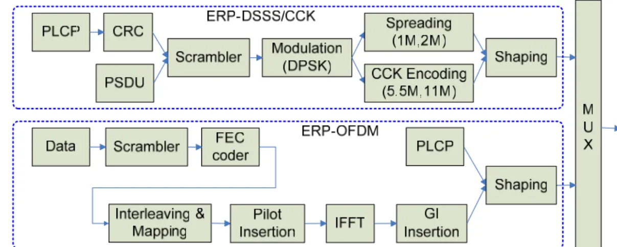
The 802.11g PHY defined in standard is known as the Extended Rate PHY (ERP), operating in the 2.4 GHz ISM band. Four operational modes are listed as followed:
A. ERP-DSSS/CCK – This mode builds on the payload data (PSDU) rates of 1, 2, 5.5, and 11 Mbit/s that use DSSS (DBPSK and DQPSK), CCK and optional PBCC modulation, and the PLCP Header operates on data rate 1 Mbit/s DBPSK for Long SYNC, 2 Mbit/s DQPSK for Short SYNC. Figure 2.1 shows the format for the interoperable PPDU that is the same with 802.11b PPDU format, and the details of components such as spreading code, scrambler, CRC implementation, and modulation refer to 802.11b standard.
Figure 2.1 Frame format of ERP-DSSS/CCK
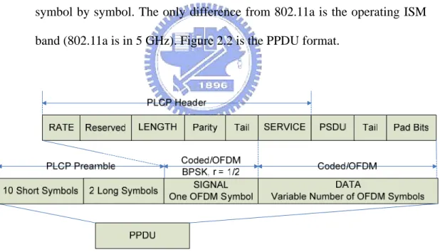
B. ERP-OFDM – This mode builds on the payload data rates of 6, 9, 12, 18 24, 36, 48, and 54 Mbit/s, based on different modulations (PSK and QAM) and coding rate, by means of OFDM technique. Except PLCP Preamble, SIGNAL field with data rate 6 Mbit/s and DATA are packaged (OFDM) symbol by symbol. The only difference from 802.11a is the operating ISM band (802.11a is in 5 GHz). Figure 2.2 is the PPDU format.
Figure 2.2 Frame format of ERP-OFDM
C. ERP-PBCC – This mode builds on the payload data (PSDU) rates of 22 and 33 Mbit/s and it is a single-carrier modulation scheme that encodes the payload using 256-state packet binary convolutional code. The PPDU format follows mode a).
D. DSSS-OFDM – This mode is a hybrid modulation combining a DSSS preamble and header with an OFDM long preamble, signal field and payload transmission. In the boundary between DSSS and OFDM parts, it is single carrier to multi-carrier transition definition. The payload data rates are the same with those of b). The PPDU format is as followed in figure 2.3.
Figure 2.3 Frame format of DSSS-OFDM
An ERP BSS is capable of operating in any combination of available ERP modes and Non ERP modes. For example, if options are enabled, a BSS could operate in an ERP-OFDM-only mode, a mixed mode of ERP-OFDM and ERP-DSSS/CCK, or a mixed mode of ERP-DSSS/CCK and Non-ERP. Notice that since the first two modes are required to implement and considered as main operating modes and the others are optional, the discussion of platform will be located on the first two modes hereinafter.
Figure 2.4 is the transmitter block diagram. After the parameters of data rate and data length are decided, following the blocks one by one will generate the transmitted signals, and the MUX that depends on operation mode will select the signal that be sent to air by antenna after up-conversion the baseband signals to operating channel frequency.
Figure 2.4 Block diagram of transmitter
2.4 Channel Model
There are many imperfect effects during transmitted signals through channels, such as Additive White Gaussian Noise (AWGN), carrier frequency offset (CFO), multi-path, and so on. These imperfections make the receiver design hard because it caused received signal distortion, rotation, delay, decay, and so on. We show the block diagram of channel model in figure 2.5, and describe these effects briefly in the following subsections.
TX RX
Multipath Path
Loss AWGN
CFO Clock Drift
Figure 2.5 Block diagram of channel model
2.4.1 Additive White Gaussian Noise
The common wideband channel thermal noise impairment, on which SNR (Signal to Noise Ratio) is typically based. The primary spectral characteristic of
thermal noise is that its power spectral density is the same for all frequencies of interest in most communication systems. The thermal noise is usually modeled as Additive White Gaussian Noise (AWGN).
2.4.2 Carrier Frequency Offset
Carrier Frequency Offset (CFO) is caused by the local oscillators’ inconsistency between the transmitter and receiver. The received signals r(t) can be written as
2
( )
( )
i ftt
r t
=
∑
s t
×
e
πΔ +θ(2-1) whereΔ andθ are the differences of carrier frequency and carrier phase between TX f
and RX, respectively. CFO will cause the constellation of the transmitted signal become a circle, that means phase of the transmitted signal will rotate with time.
2.4.3 Multi-path
Because there are obstacles and reflectors in the wireless propagation channel, the transmitted signal arrivals at the receiver from various directions over a multiplicity of paths. Such a phenomenon is called multi-path. It is an unpredictable set of reflections and/or direct waves each with its own degree of attenuation and delay. Multi-path is usually described by two sorts:
A. Line-of-sight (LOS): the direct connection between the transmitter (TX) and the receiver (RX).
LOS NLOS
NLOS
Tx Rx
Figure 2.6 NLOS and LOS between transmitter and receiver
Multi-path will cause amplitude and phase fluctuations, and time delay in the received signals. When the waves of multi-path signals are out of phase, reduction of the signal strength at the receiver can occur. One such type of reduction is called the multi-path fading; the phenomenon is known as “Rayleigh fading” or “fast fading.” A representation of Rayleigh fading and a measured received power-delay profile are shown in figure 2.7. Besides, multiple reflections of the transmitted signal may arrive at the receiver at different times; this can result in inter symbol interference (ISI) that the receiver cannot sort out. This time dispersion of the channel is called multi-path delay spread that is an important parameter to access the performance capabilities of wireless systems. A common measure of multi-path delay spread is the root mean square (rms) delay spread. For a reliable communication without using adaptive equalization or other anti-multi-path techniques, the transmitted data rate should be much smaller than the inverse of the rms delay spread (called coherence bandwidth).
Figure 2.7 Instantaneous impulse responses
2.4.4Sampling Clock Offset
The interfaces of RF and Baseband data are Digital to Analog Converter (DAC) in the transmitter and Analog to Digital Converter (ADC) in the receiver side. The ADC is the first stage of Base band, so it dominates the receiving signal to noise ratio (SNR). To get the highest input SNR, the ADC is hoped to sample at the eye open position where it has the maximum signal power. However, the initial sampling phase could be anywhere in the eye diagram, so timing synchronization is necessary. The ADC has two kinds of clock source: free running clock and phase lock loop (PLL) output clock. With free running clock, this method also called non-synchronous sampling or fix sampling, clock frequency and phase are fixed. Once timing error estimated, the compensation would be performed with interpolator. With PLL output clock, also called synchronous sampling or dynamic sampling, it receives the timing error and adjusts its frequency and phase to compensate the error. There is a need to
maintain synchronization while the accuracy and stability of the original clock reference in the receiver may not be ideal. These tasks are the responsibility of a specific module Delay Lock Loop (DLL).
0 50 100 150 200 -1.5 -1 -0.5 0 0.5 1 1.5 sampling point va lu e Transmitter Receiver
Figure 2.8 Sampling clock may no ideal in the receiver
2.4.5 Path Loss
Because the signal power will decrease with the distance between TX and RX increasing, at the RX amplifier that needed is called Variable Gain Amplifier (VGA) to enhance the received signal power. If not, the wireless system will difficultly detect any signal. Assume that the transmitted signal is s(t) and the received signal is r(t), then path loss effect can be modeled as
( )
( )
_
r t
=
s t path loss
i
……….………(2-2)If the path loss is very crucial, the receiver will be not able to detect any signal without VGA. However it is difficult to know that how exact the path loss is. So the goal of AGC is to estimate the suitable path loss effect and justify the VGA gain to let the system work under the situation of having steady signal.
CHAPTER 3
TIMING SYNCHRONIZATION
3.1 System model
For our system, the PN correlator output is very important to achieve the timing synchronization. In 11b/g system we use barker code to do the timing synchronization. Peak is the maximum correlator power of one symbol time.
2
_ (Re( ( ) ) Im( (
Peak power=Max r t−nT Bi + r t−nT B)i ) )2 ……….…..(3.1) T means the one symbol time here. R t is received signal ( )
(2 )
( ) ( ( ( )) ( ) j ft ( )) _
R t = s t−τ t ⊗h t ei πΔ +θ +n t ipath loss………...(3.2) ( )
S t is transmit signal h t( ) is the effect of multipath
f
Δ is CFO,θ is phase offset, ( )τ t is clock sample rate , n t( ) is AWGN
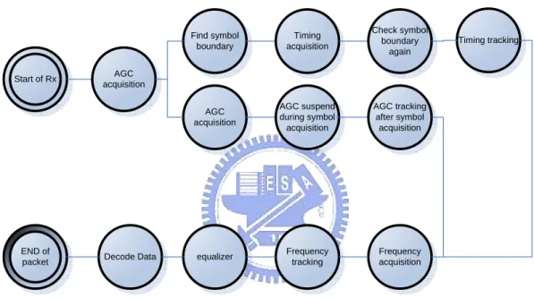
Therefore, the channel model consists of AWGN, CFO, SCO, multipath and pathloss. Then we talk about the receiver. In the proposed platform, the first step is to detect the packet, then doing the AGC acquisition and symbol boundary decision. The packet detection, AGC acquisition algorithm and symbol boundary decision was proposed by the Shih-Lin Lo. The timing synchronization was followed by the symbol boundary decision Timing synchronization includes two parts, the one is timing acquisition, and another one is timing tracking. Timing acquisition is fast to get the nearly optimum sampling clock phase. Timing tracking is to keep the optimum sampling clock phase. In my thesis, I proposed the effective timing synchronization algorithm against the all channel effect. The timing synchronization algorithm for DSSS system was described in section 3.2 and 3.3. And the timing synchronization algorithm for OFDM system was described in section 3.4.
The AGC is the another important part in my thesis. After the timing acquisition, I will check the symbol boundary again to make sure the AGC tracking correctly. I will explain the AGC design issues in the 3.3.The figure 3.1 is the state diagram of 802.11b/g receiver. Then AFC will begin to estimate the CFO and compensate the phase error. Equalizer can estimate the channel effect and compensate, too. Finally, the system will decode the data.
Start of Rx AGC acquisition Find symbol boundary AGC acquisition Timing acquisition AGC suspend during symbol acquisition Check symbol boundary again AGC tracking after symbol acquisition Frequency acquisition Frequency tracking equalizer END of
packet Decode Data
Timing tracking
Figure 3.1 state diagram of receiver
3.2 acquisition algorithm
3.2.1 1X sampling rate acquisition algorithm
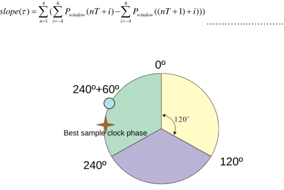
We proposed the 1x sampling rate acquisition algorithm. To improve the system performance, lower the power of ADC and reduce the sampling rate. This algorithm takes 120 degrees as the difference to sample the phase. And the algorithm adjust to optimum phase depend on the power of sampling phase.
Depend on the sampling interval of 120 degrees; we can adjust the phase location by the formula of slop. Slop definition:
………….…………...(3.3) 4 6 6 1 4 4 ( ) ( window( ) window(( 1) ))) n i i slopeτ P nT i P nT i = =− =− =
∑ ∑
+ −∑
+ +Figure 3.2 sampling location and best sample clock phase
0º
120º
240º
240º+60º
Best sample clock phase
We use the formula of slope to adjust phase location. The slope referred to these functions:
_1 ( _ / 2) ( )
slope = poewr decision region −pwer boundary ….…………..…….... (3.4) _ 2 ( ) ( _ / 2)
slope = power boundary − power decision region ………...………... (3.5)
_ 3 ( ) ( )
slope = power boundary −power boundary …………..………... (3.6) We need the three pointer of slope to adjust the phase. The algorithm use the slope_1 and slope_2 to decide that the sampling phase location exist in the optimum range or not. The slope_3 decide the method of adjust. Ex: the direction of adjust. Fast or slow
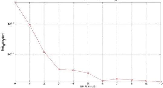
Use this algorithm on SNR=5db, Packet number is 100 and IEEE multipath channel. The phase error is almost greater than minus five and smaller than five. The performance of the 1x sampling rate acquisition is better than the 2x sampling rate acquisition in the figure 3.3. Finally the state diagram of the total algorithm show in the figure3.4
Figure 3.3 The sample clock phase error after 1X timing acquisition method
Figure 3.5 The state diagram of 1X timing acquisition
3.3 Tracking algorithm for DSSS/CCK system
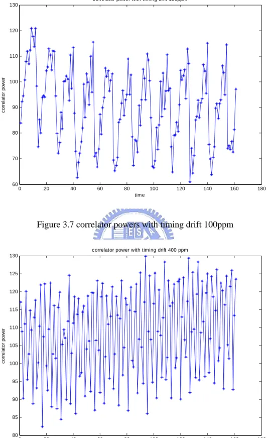
clock offset. The figure3.6 shows the correlator power with perfect channel. We can observe that the correlator power is almost the same. The figure3.7 show the correlator output with timing drift 100ppm channel. The figure3.8 show the correlator output with timing drift 400ppm channel. The figures 3.7 and 3.8 show the correlator output will swing more when the effect of timing drift is more.
0 20 40 60 80 100 120 140 160 180 120.4 120.5 120.6 120.7 120.8 120.9 121 121.1 121.2 121.3 121.4 time c o rrel a to r pow er
correlator power with perfect channel
0 20 40 60 80 100 120 140 160 180 60 70 80 90 100 110 120 130 time c o rrel a to r pow er
correlator power with timing drift 100ppm
Figure 3.7 correlator powers with timing drift 100ppm
0 20 40 60 80 100 120 140 160 180 80 85 90 95 100 105 110 115 120 125 130 time c o rrel a to r pow er
correlator power with timing drift 400 ppm
Figure 3.9 FSM of algorithm
Figure 3.9 show the tracking algorithm FSM. After the acquisition complete, the tracking algorithm in DSSS will execute first. Tracking algorithm will execute until the preamble is over. And FSM will check modulation type when preamble is over. If the datarate is 1M or 2M then the tracking algorithm in DSSS is chosen to execute. But if the datarate is 5.5M or 11M then the tracking algorithm in OFDM is chosen to execute until the packet is over.
3.3.1 Tracking algorithm for DSSS
Due to the sampling clock offset effect, we need to do the timing synchronization. In addition to the timing acquisition, timing tracking is a must in our system. This part
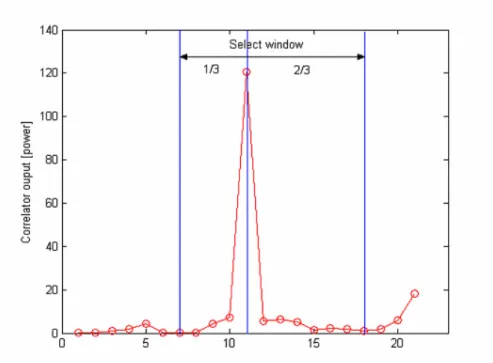
describes the tracking algorithm for the Dbpsk. Here we try to keep the phase after timing acquisition. We get the best phase location after the acquisition, and then we can save the 32 symbol’s correlator output. And we take the 32 symbol’s correlator output as the reference power. When we collect the reference power, we will adjust the phase in the steady speed. If we don’t adjust the phase in the steady speed, we will lose the best phase location after collect the reference power. Due to the swing of the power, we need to check the buffer is bigger enough or not to save the latest symbol’s correlator output. Here we take 16 as the size of buffer to collect the latest 16 symbol’s correlator output. We check the error function each 4 symbols. We will adjust the sampling clock phase when detect the timing error. In order to reduce the influence of multipath , we doesn’t take the peak power as the correlator power but to take the first one-third to last two-third correlator output as the correlator power..
The error function formula is:
..………... (3.7) 16 2 2 1 pow
(
(Re( (
) )
Im( (
) ) ))
( )
Ref
16*
iMax
r t nT iT B
r t nT iT B
e
G
τ
=− +
+
− +
=
∑
−
i
i
………..…... (3.8) 32 2 2 1 pow ( (Re( ( ) ) Im( ( ) ) )) Ref 32* i Max r t nT iT B r t nT iT B G = − + + − + =∑
i iWhere Refpow is the reference power for our algorithm and G is the current VGA Gain
We will discuss the effect of AGC later.
Figure 3.10 correlator output select window
We can know that the sampling clock phase approach the optimum sampling clock phase when the error function value is bigger than zero. Because this is meaning that the current 16 correlator power is bigger than the Refpow. If the sampling clock
phase is not in the optimum sampling clock phase, the correlator output will degrade quickly. Hence we will adjust the phase when error function smaller than zero.
3.3.2 Tracking algorithm for CCK
In the802.11b\g system, CCK modulation is used under the datarate 5.5M and 11M.Unlike the daterate1M and 2M, CCK modulation is not robust to multipath. So the simulation environment does not include the multipath. This part describes the tracking algorithm for the CCK modulation. CCK modulation does not the same as the Dbpsk modulation has the PN-code property. The tracking algorithm for the CCK takes the MAX power of Fast Walsh Transform (FWT). After the preamble, we collect the 16 symbol’s max power of FWT. And we take the current 8 max power of FWT to compare with the RefCCKpow. The error function formula is:
………... (3.9) 8 1 C C K p o w
( )
R e f
8 *
F W T i C C KP
e
G
τ
=
∑
=−
16 1 CCKpowRe f
16 *
FWT iP
G
==
∑
………...…... (3.10) Where RefCCKpow is the reference power for our algorithm and G is the current VGAGain We will discuss the effect of AGC later. The best sample timing is located at where . We can know that the sampling clock phase approach the optimum sampling clock phase when the error function value is bigger than zero. When we take the RefCCKpow as the reference power to adjust the phase, We need to use the
RefCCKpow carefully. If we take the RefCCKpow directly, we will find that the tacking
speed will too fast. In order to solve this problem, we need to take the RefCCKpow*0.9
as the new RefCCKpow. And then we can find that ( )eτ > is meaning that the current 0
8 FWT max power is bigger than the RefCCKpow. If the sampling clock phase is not in
the optimum sampling clock phase, the correlator output will degrade quickly. Hence we will adjust the phase when error function smaller than zero. The Figure 3.11 shows the situation after timing tracking. The x axis represents time and y axis represents sampling location. The time that between 0 to 160 is Bpsk modulation and 161 to the end is CCK modulation. In the beginning, we use the 3.3.1 algorithm until the preamble is over. When the preamble is over, we will check the modulation type and do the relative algorithm. The 64 means the best sampling clock phase location. We can observe that the sampling clock phase keep within 4.
( ) 0
Figure 3.11 sampling clock phases with tracking algorithm
3.3.3 AGC for DSSS/CCK
In this section, i will introduce the AGC in the DSSS/CCK system. First I will describe the algorithm that proposed by the Shih-Lin Lo. Then I will explain the new algorithm that proposed by me.
3.3.3.1AGC for DSSS
This part is proposed by Shih-Lin Lo. In the real world, we don’t know how much the effect of path loss is. No matter the received signals are noise or data, we will set the AGC (auto gain control) gain to maximum in the beginning.
10
'
10 log (
M
)
G
G
D
Where G means the VGA gain and G’ is the next VGA gain. M is the estimated barker correlator power and D is the expected barker correlator power. There are two methods for getting barker correlator power. One is measuring the peak power
10
_
'
10 log (
_
)
Peak
power
G
G
D
peak
= − i
………(3.12) 2 2 10 (Re( ( ) ) Im( ( ) ) ) 10 log ( ) _ Max r t nT B r t nT B G D peak − + − = − i i i, the other is measuring the mean power.
10
( _ _
' 10 log (
_
Sum correlator output power k G G D avg = − i ) ) 2 2 10 (Re( ( ) ) Im( ( ) ) ) 10 log ( ) _ Sum r t nT B r t nT B k G D avg − + − = − i i i …………..……....(3.13) Where k is the number of chips in one symbol. D_peak and D_avg are the expected peak power and mean power respectively. Unlike the DSSS system, the CCK system does not have the PN property. Therefore, the algorithm proposed by Shih-Lin Lo is not suitable for the CCK modulation. I will propose the new algorithm suitable for the CCK modulation.
3.3.3.2AGC for CCK
I will use the concept form the Shih-Lin Lo. Although CCK modulation does not have the PN property, we can use the FWT. The FWT function was used to construct the CCK demodulation. I will use the FWT to make AGC work correctly under CCK modulation. In this method, we get max power of FWT, and take it to do the AGC tracking. First I collect the 4 max power of FWT. Then I compare this value to the D_PFWT .D_PFWT is 95% of max power after FWT in perfect channel. We can use the
is the current VGA gain. 4 1 10 4 ' 10 log ( _ FWT i i FWT P G G D P = = −
∑
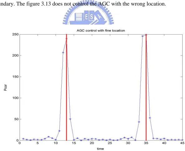
i ) ………..………....(3.14) After the introduction of AGC in DSSS and CCK, I want to talk something about the design issues. The problem is when to control the AGC. In DSSS system, data is multiplied by the barker code. If we does not adjust the VGA gain on the symbol boundary. It will make the peak power hard to believe. Then the other function that use the PN property, can’t work correctly. The figure 3.12 and figure 3.13 show the two situations to control the AGC. The figure 3.12 controls the AGC on the symbol boundary. The figure 3.13 does not control the AGC with the wrong location.Figure 3.13 AGC control with the wrong location
In order to check the influence of when to adjust VGA gain, I do the two simulations under the effect of pathloss is constant. The figure 3.14 shows the variations of VGA gain with the fine location. It can observe easily that the pathloss is 25dB. If we adjust the VGA gain with the wrong location, it will make the figure 3.15. We can compare the figure3.15 with the figure3.14, and we can observe that the variations of VGA GAIN in the figure3.15 are serious more. This is the serious problem in our system. When the VGA gain does not work correctly, functions followed by the AGC does not work correctly, too. Therefore we will check the symbol boundary before AGC acquisition and after timing acquisition. In the figure 3.16 we can see AGC acquisition follow by the packet coming. Timing acquisition is followed by the AGC acquisition. And AGC will suspend during timing acquisition. After the timing acquisition, I will do symbol boundary check again. Then AGC tracking can work correctly. Figure 3.16 show the state diagram of AGC. It describe the state of AGC and which formula to use when AGC work. The main difference between the AGC algorithms proposed by Shih-Lin Lo and the AGC algorithms proposed by me is that
the AGC algorithms proposed by Shih-Lin Lo are not suitable for CCK modulation. Therefore, I will check the modulation type after the preamble is over. Depend on modulation type to choose suitable formula for AGC.
Figure 3.14 Coherent with symbol bound
Figure 3.16state diagram of AGC
Another important issue is parameter G in the proposed tracking algorithm. We need to consider the AGC When we compare the latest correlator output with Refpow.
If the correlator outputs degrade, the AGC will adjust the VGA gain to high. Because the AGC will adjust the VGA gain, we don’t adjust the phase even if the sampling clock phase is not near the optimum sampling clock phase. Figure 3.17 show the timing synchronization without AGC gain normalization. Figure 3.18 show the timing synchronization with AGC gain normalization. From these two figures, we can observe that when the correlator powers degrade, the AGC will adjust the VGA gain to high in figure 3.17. The data in figure 3.18 is the same as figure 3.17.But the data in figure 3.19 was normalized by the parameter G. Hence we don’t do the gain normalization; we have no idea to know when the sampling clock phase is not near optimum sampling clock phase. So we use the parameter G to solve this problem. When we use the parameter G in the proposed timing tracking system, I can find out the timing error easily. Figure 3.19 show the effect of timing synchronization without AGC gain normalization. It will make the timing synchronization hard to work
correctly. In the figure 3.19 the location 128 is the best location to sample the clock. WE can see the timing error is serious with the time going. Figure 3.20 show the timing synchronization with AGC gain normalization. Then we can see the sampling clock phase within the optimum location.
Figure 3.17 timing synchronization without AGC gain normalization
Figure 3.19 timing synchronization without AGC gain normalization
3.4 TIMING SYNCHRONIZATION for OFDM
system
Frame detection Timing acquisition Auto frequency
control FFT
Channel
estimation Qam demapping De - interleaver Viterbi decoder Receive Data in
decode Data out AGC
Figure 3.21 Block diagram of 11a/g PHY system
Figure 3.21show the black diagram of 11a/g system. In the OFDM system, the timing synchronization needs to be completed during short preamble. Unlike the 802.11b/g, the 802.11a/g has 10 short preambles only. We need to use fewer preambles to achieve the timing acquisition. Here we use the property of PN code, the correlator output would be max when two PN code in phase only .Hence I will use normalized cross correlation to do timing synchronization in OFDM system. Like the figure3.22, we take the short preamble data to multiply the receive data, and calculate norm of short preamble and receive data, then C divided by the N equals P. And P is the normalized power.
……….…....(3.15) *
(
) *
(
(
) /
k k k kC
S
R
N
n o r m
S
n o r m
R
P
a b s C
N
=
⋅
=
=
∑
)
(4 arg(
( )))*( 90 )
iPhase
= −
Max P
−
………....(3.16) Where Pi is the normalized cross correlator power. The formula (3.16) is used tocalculate the timing error, then use it to compensate the timing error.
S hort T raining S equence S hort T raining S equence S hort T raining S equence S hort p ream b le C orrelate
Figure 3.22 Relation between short preamble and short training sequence
Figure 3.23 sampling phase diagram
The figure 3.26 shows the all steps of the proposed timing synchronization algorithm. After the packet is detected, we can collect the normalized power of the first short preamble, then shift the 90 degree each short preamble and save the normalized power of the short preamble each short preamble. Here I take the sampling phase as a circle. Like the figure3.23, this is meaning that we can coarse estimate the normalized power of each phase. When preamble_count is equal to 3, we will check the normalized
power of the four short preambles, then choose the best one and adjust the sampling clock phase location.
We get another problem here, if we enable the AFC directly after the timing acquisition, the AFC will get the two preambles that preamble_count is equal to 2 and 3. But short preamble 2 and 3 are the measure data in the timing acquisition. Therefore we need two short preambles that in the optimum sampling phase for AFC to estimate the CFO and phase error. In order to make sure that AFC can use two optimum sampling phase preambles to do the auto-correlation, we will wait two preambles for AFC. Figure 3.22 shows the sample clock phase error after this timing synchronization method. Simulation situation:
SNR = 17, Data rate =36, Packet NO = 100, PSDU length =1000 bytes CFO = 50 ppm, path loss = -25 dB, IEEE multipath RMS = 50 tap = 6
Figure 3.24 the sample clock phase error after this timing synchronization method Simulation situation:
SNR = 20, Data rate =54, Packet NO = 100, PSDU length =1000 bytes CFO = 50 ppm, path loss = -25 dB, IEEE multipath RMS = 100 tap = 6
Figure 3.25 the sample clock phase error after this timing synchronization method The Figure 3.22and Figure 3.23 show the phase error after our timing synchronization algorithm. We can observe that the max phase error is 6. Because the upsampling rate is 22, and the 22 divided by 4 equals 6.And 360 degree divided by the 90 degree equals 4. Hence we can evaluate the timing error is 6. Then the simulation results are matching my idea.
Table 5.1 Comparison state-of-the-art timing synchronization You-Hsien Lin[10] traditional[12][13] This work
Method Dual correlator
differential based interpolator Dynamic sampling Sampling Rate 2 times 2 times 1 times
Modulation DSSS OFDM DSSS/CCK/OFDM SCO tolerance
range SCO from 25 to - 25 N/A SCO from 400 to - 400 From the table 5.1 we can observe that the main advantage of the proposed algorithm is the sampling rate, and SCO tolerance range. The main reason of the proposed algorithm tolerate the SCO range from 400 to – 400 is that the proposed algorithm not only has the acquisition but also tracking mechanism.
S t a r t S u s p e n d t w o p r e a m b l e D e p e n d o n t h e f o u r P e a k p o w e r t o a d j u s t t h e P h a s e P a c k e t d e t e c t i o n C o l l e c t c o r r e l a t o r p o w e r o u p u t A n d s h i f t = 9 0 º p h a s e
Figure 3.26 state diagram of timing synchronization
N O P a c k e t c o m i n g P r e a m b l e _ c o u n t = 3 N O Y E S Y E S S t a r t A F C
CHAPTER 4
SIMULATION RESULTS
4.1 Simulation tool
First we need to choose a suitable tool. Two languages, C/C++ and Matlab are the nice choices, because these two languages have a lot of advantages during the process of constructing platform. These advantages are listed below
a. Complete standard library and document of help b. Easy to learn programming style
c. High simulation speed
d. Quickly algorithm verification e. Co-simulate with Verilog f. Easily porting to HDL
Matlab is chosen as the suitable tool to construct the system platform for the reason of powerful matrix and mathematic functions, friendly Graphical User Interface (GUI), simple debugging tool and many different kinds of figure plotting functions. Although C/C++ has the highest simulation speed, but lack of mathematical functions and less friendly GUI cause us give up it to choose Matlab as the tool. Figure 5-1 shows the block diagram of whole system. All important system parameters could be seeing in this figure. There three components in this system, transmitter, channel and receiver, and a top file is used to control these three components and call them. The top file controls a parameter-packet number, that parameter defines how many packets the system will execute at the same conditions with increasing SNR.
Figure 4.1 System block diagram
4.2 Simulation results
4.2 simulation results
4.2.1 DSSS/CCK part simulation results
In order to know the performance and tolerate range of my algorithm, I will simulate 2Mbps for DSSS part and 11Mbps for CCK part. AWGN, multipath, CFO, SCO and path loss effects are simulated in our system. For the DSSS part, the simulation environment has AWGN, CFO, multipath and path loss. Simulation results are simulated with 100 packets, 1000 bytes, IEEE multipath rms 50ns, CFO 50 ppm, and SCO 50 ppm and pathloss 25 dB. Figure 4.2 shows the PER of 2 Mbps with perfect synchronization, 1x acquisition with tracking and 1x acquisition without tracking. The performance loss is almost 1dB under the SCO effect.
Figure 4.2 PER of 2Mbps
Figure 4.3 shows the BER of 2 Mbps with perfect synchronization, 1x acquisition with tracking and 1x acquisition without tracking.
AWGN, CFO, SCO and path loss effects are simulated in our system. For the CCK part, the simulation environment has AWGN, CFO and path loss. Simulation results are simulated with 500 packets, 1000 bytes, CFO 50 ppm, and SCO 50 ppm and pathloss 25 dB. Figure 4.4 shows the PER of 11 Mbps with perfect synchronization, 1x acquisition with tracking and 1x acquisition without tracking. The performance loss is almost 1dB under the SCO effect. Figure 4.5 shows the BER of 11 Mbps with perfect synchronization, 1x acquisition with tracking and 1x acquisition without tracking.
Figure 4.5 BER of 11Mbps
Figure 4.6 and Figure 4.7 show the SCO range that synchronization algorithm for DSSS/CCK can tolerate. The tolerate range is almost in the 400 to -400. From Figure 4.6 and 4.7, our system will meet the requirement that per is smaller than 1/10 under SCO 50 ppm.
Figure 4.7 SCO range that synchronization algorithm can tolerate
4.2.2 OFDM part simulation results
AWGN, multipath, CFO, SCO and path loss effects are simulated in our system. The simulation environment has AWGN, CFO, multipath and path loss. Simulation results are simulated with 1000 packets, 1000 bytes, rms 50ns, CFO 50 ppm, and SCO 50 ppm and path loss 25 dB. Figure 4.8 shows the PER of 36 Mbps with perfect acquisition, 1x acquisition and random initial phase without acquisition. Figure 4.9 shows the BER of 36 Mbps with perfect acquisition, 1x acquisition and random initial phase without acquisition. We can observe that the performance loss is about 1dB under the SCO effect.
Figure 4.8 PER of 36Mbps
Figure 4.9 BER of 36 Mbps
to 24 dB, rms 50 ns, CFO 50 ppm, SCO 50ppm and path loss -25 dB. Figure 4.10 shows the PER of 54 Mbps with perfect acquisition, 1x acquisition and random initial phase without acquisition. Figure 4.11 shows the BER of 54 Mbps with perfect acquisition, 1x acquisition and random initial phase without acquisition. The performance loss is about 1dB. The per curve will meet the standard at SNR22.
Figure 4.11 BER of 54 Mbps
Figure 4.12 shows the SCO range that synchronization algorithm can tolerate under datarate is 36M. Simulation results are simulated with 1000 packets, 1000 bytes. Simulation environment is IEEE Multiath RMS 50ns,CFO 50 ppm and pathloss -25dB Simulated SCO range are -800 -400 -200 -50 50 200 400 800. In our system, the tolerate range is from 400 to – 400.
Figure 4.12 SCO range that synchronization algorithm can tolerate
Figure 4.13 shows the SCO range that synchronization algorithm can tolerate under datarate in 54M. Simulation results are simulated with 500 packets, 1000 bytes. Simulation environment is IEEE Multiath RMS 50ns,CFO 50 ppm and pathloss -25dB Simulated SCO range are -800 -400 -200 -50 50 200 400 800. In our system, the tolerate range is from 400 to – 400.
CHAPTER 5
Proposed Hardware
5.1Matlab to Verilog Design Flow
Figure 5-1 shows the proposed platform design flow from Matlab simulation to hardware implementation. The first step of system design is chosen the suitable algorithm to avoid the channel effect. The second step is measured the proposed algorithm work well, then design architecture. System specifications need to check and performance should be maintained. Hence change the high level function description block to low level architecture hardware model one by one. The Matlab hardware models are built and system simulation is performed to keep the performance. After deciding the architecture, we have to perform the fixed point simulation, then design the HDL code that match the matlab code. And I use the same test bench as the matlab code to simulate HDL code. If the result does not match the match matlab result, we will modify the code and check the float-point simulation. This is a trade-off between the hardware cost and system performance.
5.2
Design Architecture
Figure 5-2 illustrates the block diagram of dynamic sampling. The clock source is the DLL output. Different from the usual, the proposed DLL is implemented with all-digital circuits, and replaced by all-digital delay lock loop (ADDLL) [10] which has the same function and similar architecture as DLL. ADDLL would adjust the sampling clock frequency and phase directly once the timing error is estimated.
Figure 5-2 the block diagram of dynamic sampling
The timing synchronization has two parts in DSSS system. The one is timing acquisition, another one is timing tracking algorithm. In OFDM system, the timing synchronization has timing acquisition only. The timing tracking part replaces by the AFC. The whole system of the proposed algorithm can be divided three parts, the OFDM timing acquisition, DSSS timing tracking and CCK timing tracking. At first, the data are saved into 16-element shift registers. The timing algorithm for DSSS, the timing algorithm for OFDM and timing algorithm for CCK share the shift registers.
Figure 5-3 the block diagram of DSSS/OFDM/CCK timing synchronization
5.3 Proposed hardware component
Figure5.4 shows the Architecture of timing tracking algorithm for DSSS modulation. The architecture of timing tracking algorithm for DSSS can be implemented with the formula (3.7).In the proposed architecture, we use the 2 adder and 2 multiplier, and a lot of the registers. The data that samples by the ADC were saved in the DATA_FIFO. The 11 XORs are used to achieve that receive data multiplied by the barker code. The square part can be implementing with Look-up Table(LUT) rather than multiplier to reduce hardware cost. Then the FIFO_1 and FIFO_2 are use to save peak powers, and I use the two adders, two multipliers to calculate the Current peak power Refpow. Here I use the 3 inputs adder rather than the
32 inputs adder to reduce the hardware cost. Like the accumulator, we add the new coming power, and we minus the 32 power to achieve the function of 32 inputs adder. Finally use the one comparator to calculate the final results, and then transmit the result to the ADDLL to sampling the optimum location.
Figure 5.4 Architecture of timing algorithm for DSSS modulation
Figure5.5 shows the Architecture of timing tracking algorithm for CCK modulation. The architecture of timing tracking algorithm for CCK can be implemented with the formula (3.8).And the architecture of timing tracking algorithm for CCK is almost the same as the Figure 5.3.In the proposed architecture, we use the 2 adder and 2 multiplier. Unlike the DSSS algorithm, we need on e buffer to save the input Data only.Then the FIFO_1 and FIFO_2 are use to save the max power of FWT, and I use the two adders, two multipliers to calculate the Current peak power Refpow. The same idea as the Architecture for DSSS, we use the 3 inputs adder to
reduce the hardware cost. Finally use the one comparator to calculate the final results.
ADC_in DATA_FIFO 11 regs ( )2 LUT C M P Barker code 2 2 (Re( ( ) ) Im( ( ) ) ) Max r t−nT Bi + r t−nT Bi VGA ADDLL D D 11 1 Current peak power Refpow D D D D 16 2 2 1 ( (Re( ( ) ) Im( ( ) ) )) 16 * i Max r t nT iT B r t nT iT B G = − + + − +
∑
i i 32 2 2 1 ( (Re( ( ) ) Im( ( ) ) )) 32 * i Max r t nT iT B r t nT iT B G = − + + − +∑
i i FIFO_1 32 regs FIFO_2 16 regs D LUT 1/ G D DADC_in C M P FWT P VGA ADDLL BUffer FWT Current peak power
Ref
pow FIFO_1 16 regs FIFO_1 8 regs ADC_in C M P FWT P VGA BUffer FWTRef
pow FIFO_1 16 regs FIFO_1 8 regs ADC_in C M P FWT P VGA BUffer FWTRef
pow FIFO_1 16 regs FIFO_1 8 regs ADC_in C M P FWT P VGA register FWTRef
pow 8 1 8* FWT i P G =∑
16 1 16 * FWT i P G =∑
FIFO_1 16 regs FIFO_1 8 regs D D D D D D LUT 1/ GFigure 5.5 Architecture of timing algorithm for CCK modulation
Figure5.5 shows the Architecture of timing tracking algorithm for OFDM. The architecture of timing tracking algorithm for CCK can be implemented with the formula (3.15).In order to reduce the hardware cost, we change the formula to
* ( ) / ( ) k k k C S R P abs C norm R = ⋅ =
∑
……….…(5.1)Because the is the fix value, then we can reduce one multiplier. In the proposed architecture, we use the 1 adder, 1 multiplier and 3 comparator. Finally transmit the comparator result to ADDLL to sample the optimum location
( k)
ADC_in DATA_FIFO 16 regs C M P Short preamble * k k C =
∑
S R⋅ ADDLL 16 1 4 3 2 1 C M P C M P ( )2 LUT 1/ ( k) N = norm S ( ) / ( k) P =abs C norm S D D DChapter 6
Conclusion and Future Work
6.1
Conclusion
In this thesis, we propose a timing synchronization algorithm that can handle successful both OFDM and DSSS packets and dynamically controlling the sampling frequency. So the 802.11g system is used to combine with the proposed systems. Another contribution of mine is that my timing synchronization algorithm work under the lower sampling rate. This is the main different point from the traditional timing synchronization algorithm. And the proposed timing algorithm can resist the multipath fading, SCO, CFO, AWGN and pathloss effect. The Timing acquisition algorithm for DSSS can converge the sampling phase between plus 4 and minus 4. The Timing acquisition algorithm for OFDM can converge the sampling phase between plus 6 and 0.The tracking algorithm for DSSS/CCK keep the optimum sampling phase within 6. Here I improve the AGC that proposed by the shih-Lin Hsu. I propose the new AGC algorithm to fit the CCK modulation, and solve the control issues for AGC, and the other issues due to AGC. The most important issue is normalized problem for tracking algorithm. I was solve this problem successfully. Finally I proposed the hardware architecture for my proposed system.
6.2
Future Work
There are some possible improvements in the future works. The ADDLL is the must of my system. So the design of ADDLL is the important part of my future work. And the tracking algorithm is not better enough; I will try to design the better timing
synchronization algorithm. For implementing a chip finally, the fixed-point simulation is needed. So, the current floating-point (algorithm level) platform must been changed to fixed-point platform. The wordlength of my proposed system must be considered carefully. Construct the HDL platform is a bog work for me to do in the future. I will complete the HDL simulation in the future work.
References
[1] “Wireless LAN Medium Access Control (MAC) and Physical Layer (PHY)”, specifications, IEEE 802.11b standard 1999
[2] “Wireless LAN Medium Access Control (MAC) and Physical Layer (PHY)”, specifications, IEEE 802.11a standard 1999
[3] “Wireless LAN Medium Access Control (MAC) and Physical Layer (PHY)”, specifications, IEEE 802.11g standard 2003
[4] Chien-Jen Hung, “A Differenctial Decoding Based Baseband Processor for DSSS Wireless LAN Applications”, NCTU, master thesis, June 2003
[5] Bernard Sklar, Digital Communications - Fundamentals and Applications Second Edition, Prentice-Hall Inc., Communication Engineering Services, Tarzana, California and University of California, Los Angeles, 2001
[6] A. L. Welti, B. Z. Bobrovsky *, “Doppler Acceleration Influence On Code Tracking In Direct Sequence Spread Spectrum Systems: Threshold Calculation And AGC Algorithms”, Global Telecommunications Conference, IEEE, 1624 - 1628 vol.3, Dallas, TX USA, Nov. 1989
[7] Peter Kreuzgruber, “A Class of Binary FSK Direct Conversion Receivers”, Vehicular Technology Conference, IEEE, 457 - 461 vol.1, Stockholm Sweden, 1994
[8] Arnold L. Welti, Member, IEEE, and Ben-Zion Bobrovsky, Member, IEEE, “On Optimal AGC Structure for Direct Sequence Spread Spectrum PN-Code Tracking”
[9] Mitsuhiko YAGYU, Shigenori KINJO and Hirohisa YAMAGUCHI, Texas Instruments Tsukuba R&D Center, “Analysis and Minimization of Loss of Process Gain with A/D Conversion in DS-CDMA”, Vehicular Technology
Conference, IEEE VTS, 2476 - 2480 vol.5, Amsterdam Netherlands, 1999 [10] You-Hsien Lin, “The Study of Dynamic Sampling Loop For Wireless
Baseband Applications”, NCTU, master thesis, August 2004
[11] Shih-Lin Lo , “The Study of Front-End Signal Process for Wireless Baseband Applications", NCTU, master thesis, July 2004
[12] F. M. Gardner, “Interpolation in digital modems–Part I: fundamentals,” IEEE Trans. Comm., vol. 41, pp. 501-507, March 1993.
[13] L. Erup, et al., “Interpolation in digital modems–Part II: implementation and performance," IEEE Trans. Comm., vol. 41,pp. 998-1004, June 1993.
[14]Xiong Liu and Alan N. Willson, Jr. “ A NEW INTERPOLATED SYMBOL TIMING RECOVERY METHOD" Circuits and Systems, 2004. ISCAS 'May 2004
[15] Won Namgoong, “ADC and AGC Requirements of A Direct-Sequence Spread Spectrum Signal", IEEE 2001 Midwest Symposium on Circuits and Systems, 744 - 747 vol.2, Dayton, OH USA, 2001