國
立
交
通
大
學
電子工程學系 電子研究所碩士班
碩
士
論
文
應用於太陽能之高效率的電源管理系統
High Efficiency Power Management System For Solar
Energy Harvesting Applications
研 究 生:吳俊毅
指導教授:黃 威 教授
應用於太陽能之高效率的電源管理系統
High Efficiency Power Management System For Solar
Energy Harvesting Applications
研 究 生:吳俊毅 Student:Chun-Yi Wu
指導教授:黃 威 教授 Advisor:Prof. Wei Hwang
國 立 交 通 大 學
電 子 工 程 學 系 電 子 研 究 所
碩 士 論 文
A Thesis
Submitted to Department of Electronics Engineering & Institute of Electronics College of Electrical Engineering and Computer Engineering
National Chiao Tung University in partial Fulfillment of the Requirements
for the Degree of Master
in
Electronics Engineering September 2009
Hsinchu, Taiwan, Republic of China
應用於太陽能之高效率的電源管理系統
學生:吳俊毅 指導教授:黃 威 教授
國立交通大學電子工程學系電子研究所
摘 要
在本篇論文中,我們將目標放在設計並實現一個應用於太陽能之高效率的電源 管理系統。其中包含電壓調節器和交換式電容直流-直流轉換器、高電壓電荷幫 浦以及太陽能最大功率追踪控制電路設計。主要的研究成果如下: 1. 在本篇論文中提出了一個可應用於太陽能之高效率的電源管理系統。本系 統藉由太陽能採集能量,並且產生不同的電壓位準以應用於 SoC 電壓調 節 (例如:1V~0.3V 提供給類比電路和低功率數位電路,-1.2V 提供給記憶 體電路,5V 提供給 I/O 元件)。 2. 一個新的連接架構用於改善高電壓電荷幫浦的能量效益和提升負載能力 被提出。 3. 提出了一個可應用於太陽能最大功率追踪電路以控制太陽能電池位於最 大功率區域並整合至功率管理系統中,使系統可對電池補充能量,並且有 效率的利用電池的能量。High Efficiency Power Management System For Solar
Energy Harvesting Applications
Student : Chun-Yi Wu
Advisors : Prof. Wei Hwang
Department of Electronics Engineering & Institute of Electronics
National Chiao-Tung University
ABSTRACT
The goal of this research is to design and implement a high efficiency power management system for solar energy harvesting applications. This includes the design of voltage regulator and switched capacitor DC-DC converter, high charge pump and PV cell maximum power tracking control circuit. The major contributions of this thesis are list as follow:
1. A high efficiency power management system for solar energy harvesting applications is proposed. The power management system receives power from photovoltaic (PV) cell and generate different voltage levels which are suitable for SoC integrated regulator applications (such as 1V~0.3V for analog circuitry and low power digital circuitry, -1.2V for memory circuitry, and 5V for I/O components).
2. A novel connect scheme for improving power efficiency and loading capability of charge pump which generates ultra high voltage is proposed.
3. A maximum power tracking circuit for controlling PV cell in maximum power region is proposed and integrated to the power management system for solar energy harvesting applications. The power management system works with a rechargeable battery and uses the energy of battery efficiently.
Acknowledgement
感謝我的指導教授黃威教授,在自由的研究風氣下讓我對自己研究的領域有 更加深入的瞭解,並且提供優良的研究環境與充足的研究資源,讓我自由發揮想 法和創意來完成這一篇論文。感謝口試委員莊景德教授和周世傑教授在論文上的 建議和鼓勵,讓我的論文可以更加完整。 感謝維致學長培養我獨立解決問題的能力,讓我學習遇到任何問題都能靠自 己去找到答案。感謝柏蒼學長、明宏學長和浩義學長在研究生活上無私的分享, 讓我有了一些不同的體會。感謝同豪學長在研究上的幫忙,讓我可以承接先前的 研究成果再加以發揚光大。感謝我的好伙伴益銘、士祺和各方好友的支持與鼓 勵,讓苦悶的研究生活不再覺得孤單。 最後我要感謝我的家人對我在生活上的幫助以及精神上的支持,讓我遇到挫 折更有勇氣去面對,並且能夠順利的完成碩士的論文研究。Content
摘 要...i ABSTRACT...ii Acknowledgement...iv Content...v List of Figures...vii List of Tables...x Chapter 1 Introduction...11.1 Motivation of the Thesis ...1
1.2 Research Goals and Major Contributions...2
1.3 Thesis Organization ...2
Chapter 2 An Overview of Power Management System for Energy Harvesting Applications ...4
2.1 Photovoltaic (PV) Cell ...4
2.2 Maximum Power Tracking and Control Algorithm ...7
2.3 Ultra Low Voltage Power Management and Computation Methodology for Energy Harvesting Applications...11
2.5 A Battery Management System for Energy Harvesting Applications...20
2.6 Summary...26
Chapter 3 Switched Capacitor DC-DC Converter and Voltage Regulator ...27
3.1 Conventional Switched Capacitor DC-DC Converter...28
3.2 Stability Scheme of Voltage Regulator ...34
3.3 Voltage Regulator with Digital Buffer ...40
3.4 Switched Capacitor DC-DC Converter & Voltage Regulator ...43
3.5 Summary...55
Chapter 4 Charge Pumps...56
4.1 Voltage Doubler ...57
4.2 Dickson Charge Pump...62
4.3 Negative Voltage Generator...68
4.4 Proposed Charge pump...68
4.5 Summary...75
Chapter 5 High Efficiency Power Management System for Solar Energy Harvesting...76
5.1 The Scheme of Power Management System for Solar Energy Harvesting Applications ...77
5.2 The Overview of Power Management System for Solar Energy Harvesting Applications ...81
5.3 PV Characteristic and Detail Circuitry ...83
5.4 Simulation Results ...88
5.5 Summary...94
Chapter 6 Conclusion and Future Work ...95
List of Figures
Fig. 2.1 Equivalent circuit of a photovoltaic cell...4
Fig. 2.2 I-V and Power-V curve of PV cell under different temperature at Ig=4mA...6
Fig. 2.3 Power-V curve of photovoltaic cell under different temperature and current..7
Fig. 2.4 The characteristic curves of PV cell. ...8
Fig. 2.5 The flowchart of MPT control...9
Fig. 2.6 Ultra low voltage power management system for energy harvesting applications. ...11
Fig. 2.7 Block diagram of the power circuit. ...12
Fig. 2.8 Clock generator...13
Fig. 2.10 Circuit of the optimal power tracking unit. (①normal working phase, ② sensing phase, ③evaluation phase) ...19
Fig. 2.11 Control unit for the charge pump...20
Fig. 2.12 The battery management system for energy harvesting applications...21
Fig. 2.13 (a) Microbattery electrical model. (b) Normalized state of charge. ...21
Fig. 2.15 The architecture of micro-battery charge control circuit...23
Fig. 2.16 Battery management system with charge controller...25
Fig. 2.17 Charge controller set points. [6] ...25
Fig. 3.3 Equivalent circuit of the gain configuration with gain of 1/2...30
Fig. 3.5 Typical structure of a low-dropout regulator with an intermediate buffer stage. ...34
Fig. 3.6 Source-follower implementation of the intermediate buffer stage...35
Fig. 3.7 (a) Source-follower with shunt feedback. (b) The buffer with dynamically-biased shunt feedback for output resistance reduction under different load currents...36
Fig. 3.8 Structure of classical voltage regulator. ...39
Fig. 3.9 Loop gain of classical voltage regulator...40
Fig. 3.10 Conventional linear regulator topology. ...41
Fig. 3.11 Linear regulator with digital buffer...41
Fig. 3.12 Schematic of linear regulator with digital buffer...42
Fig. 3.13 Reference voltage circuit [17]. ...43
Fig. 3.14 The design of reference voltage circuit [17]...44
Fig. 3.15 Reference voltage circuit in this work...44
Fig. 3.16 (a) Temperature variation. (b) Power supply variation...45
Fig. 3.18 Variable voltage reference generation with temperature variation. ...46
Fig. 3.19 Schematic of switched capacitor DC-DC converter. ...48
Fig. 3.20 Schematic of switched capacitor DC-DC converter. ...49
Fig. 3.21 transient response of voltage down conversion...49
Fig. 3.22 Voltage regulator with dynamic-biased op amp. ...50
Fig. 3.23 Output voltage of voltage regulator under different Load current. ...51
Fig. 3.25 The state diagram of the finite state machine. ...53
Fig. 3.26 The schematic of switched capacitor matrix. ...53
Fig. 3.27 The topology of switched capacitor matrix. ...54
Fig. 4.1 (a) Programming: channel hot electron injection in the floating gate at the drain side. (b) Erasing: Fowler-Nordheim electron tunneling current through the tunnel oxide from the floating gate to the silicon surface...57
Fig. 4.2 Voltage doubler. ...57
Fig. 4.3 Cockcroft-Walton voltage multiplier...58
Fig. 4.4 Four stage boosted charge pump for positive high voltage generation with n-MOS transfer gates and conventional four-phase clocking scheme...59
Fig. 4.5 Voltage doubler[24]. ...60
Fig. 4.6 (a) Stage schematic of the two-phase charge pump[25]. (b) Complete schematic of the tree-stage two-phase charge pump...62
Fig. 4.6 (a) Stage schematic of the two-phase charge pump[25]. (b) Complete schematic of the tree-stage two-phase charge pump...63
Fig. 4.8 A four-stage charge pump using static CTS’s...64
Fig. 4.9 A four-stage charge pump using dynamic CTS’s. ...65
Fig. 4.12 Dickson charge pump generates negative voltage...68
Fig. 4.13 Charge pump for improving body effect. ...69
Fig 4.16 the new charge pump connection scheme with MOS capacitor. ...71
Fig 4.18 The circuit operation for current charging...73
Fig 4.19 The transient response of the new charge pump...73
Fig. 4.20 Charge pump output voltage vs. different load current. ...74
Fig. 4.21 Power efficiency of charge pumps in different load current. ...74
Fig. 5.1 First kind scheme of power management system...77
Fig. 5.2 Leakage path of first kind scheme...77
Fig. 5.3 Second kind scheme of power management system. ...79
Fig. 5.4 Third kind scheme of power management system. ...80
Fig. 5.5 Fourth kind scheme of power management system...81
Fig. 5.6 (a) Block diagram of the overall system. (b) Architecture of the power management system. ...82 Fig. 5.7 P-V and I-V curve of PV cell. The x-axis is output voltage of PV cell. The left
y-axis is load current. The right y-axis is output power...83
Fig. 5.8 The schematic of maximum power tracking circuitry. ...84
Fig. 5.9 The schematic of multi-phase MPT circuitry. ...85
Fig. 5.10 Resistor-string DAC for variable voltage reference generation. ...86
Fig. 5.11 (a) Battery charger. (b) Negative voltage generator...87
Fig. 5.12 The high voltage charge pump. ...87
Fig. 5.13 Layout view of the high efficiency power management system for solar energy harvesting applications...88
Fig. 5.14 Single PV cell maximum power tracking transient response. ...89
Fig. 5.15 Single PV cell maximum power tracking transient response with different process corner...90
Fig. 5.16 The energy charging transient response of maximum power tracking...90
Fig. 5.18 Variable voltage reference generation with temperature variation. ...92
Fig. 5.18 The energy charging transient response of maximum power tracking...93
Fig. 6.1 The power management system with different environmental power sources. ...96
List of Tables
Table 3.1 Comparison 600mV generator of Ref.[17] and this work...45
Table 3.2 Temperature variation ...47
Table 3.3 Comparison of [15], [16] and proposed voltage regulator. ...51
Table 3.4 Comparison of linear regulator and SC DC-DC converter. ...54
Table 5.1 Temperature variation ...92
Chapter 1 Introduction
1.1 Motivation of the Thesis
In the recent years, the market of portable devices likes notebook, cell phone, PDA and smart phone is grow up rapidly and more new portable products will be developed in the near future. In the developing of portable devices, more and more functions are integrated into a product. At the same time, people concern that whether the product can use for a long time without charging the battery in charge socket. And the capacity of batteries improves relatively slowly then the power consumption of the portable devices which is integrated more and more functional blocks. So the environmental power harvesting applications can provide a charge method for overall system and extends the system life.
Due to the green power considerations and eco-awareness, the research of energy
harvesting application is getting popular. Previously, the system of tracking maximum output power of photovoltaic cell was implemented in [1]. An ultra-low voltage power management for energy harvesting applications was developed and worked with a FIR filter in [2]. With low output voltage of solar cell, a micro power management system was proposed in [3]. The micro power management system decided the working frequency of charge pump by the room lighting environment and outputted the maximum power to loading circuitry. An energy harvesting application with micro battery was also implemented in [4]. This power management circuit accepted energy from RF power and thermo generator power and outputted the power to micro battery as energy storage. A battery management system for solar energy applications was developed in [5]. The battery management system was used to increase the service life of the battery.
1.2 Research Goals and Major Contributions
The goal of this research is to design and implement a high efficiency power
management system for solar energy harvesting applications. This includes the design of voltage regulator and switched capacitor DC-DC converter, high voltage generator and PV cell maximum power tracking control circuit.
The major contributions of this thesis are list as follow:
1. A high efficiency power management system for solar energy harvesting applications is proposed. The power management system receives power from photovoltaic (PV) cell and generate different voltage levels which are suitable for SoC integrated regulator applications (such as 1V~0.3V for analog circuitry and low power digital circuitry, -1.2V for memory circuitry, and 5V for I/O components).
2. A novel connect scheme for improving power efficiency and loading capability of charge pump which generates ultra high voltage is proposed.
3. A maximum power tracking circuit for controlling PV cell in maximum power region is proposed and integrated to the high efficiency power management system for solar energy harvesting applications. The power management system works with a rechargeable battery and efficiently uses the energy of battery.
1.3 Thesis Organization
The rest of the thesis is organized as follows: an overview of solar energy harvesting applications technique is introduced in the Chapter 2. The characteristics of photovoltaic (PV) cell and a maximum peak power tracking technique are introduced.
applications is also introduced.
The techniques of improving the stability and transient response of voltage regulator are introduced in the Chapter 3. The voltage regulator and switched capacitor DC-DC converter for SoC integrated regulator applications are proposed in the Chapter 3. The voltage doubler and Dickson charge pump are introduced in the Chapter 4. The techniques of improving the pumping efficiency of charge pump are also introduced. For improving the power efficiency and loading capability of charge pump which generates ultra high voltage, a novel connect scheme is proposed in the Chapter 4.
An integrated power management system for solar energy harvesting applications is proposed in the Chapter 5. The power management system generates different voltage levels for the SoC integrated regulator applications by voltage regulator, switched capacitor DC-DC converter and charge pump. The power management system contains a maximum power tracking circuitry for controlling PV cell in the maximum power region. By utilizing multi-phase maximum power tracking, we can average the PV cell module output power and provide a constant output power for protecting the rechargeable battery.
Chapter 2 An Overview of Power
Management System for Energy
Harvesting Applications
This chapter introduces the overview of power management system for energy harvesting applications. The photovoltaic (PV) cell characteristic would be demonstrated in Section 2.1. A maximum peak power tracking system would be introduced in Section 2.2. Section 2.3 and Section 2.4 introduce two different power management systems for solar energy harvesting applications, RF and thermo-generator harvesting applications. Section 2.5 introduces the battery management system for solar energy harvesting applications. Finally, Section 2.6 is the summary.
2.1 Photovoltaic (PV) Cell
The photovoltaic cell converts the light energy into electrical energy. The photovoltaic cell is a nonlinear device which can be represented as a current source model with a PV diode, a shunt resistance (RSH), and a series resistance (RS), as
The traditional I-V cure characteristic of a photovoltaic cell, while neglecting the internal shunt resistance, is given by the following equation [6]:
{exp[
(
)] 1}
O g sat O O Sq
I
I
I
V
I R
AKT
= −
−
−
(2.1)Io and Vo describe the output current and the output voltage of the photovoltaic cell
respectively. Ig is the generated current for a given solar power, Isat is the reverse
saturation current, q is the charge of an electron, A is the ideality factor for a p-n junction, K is the Boltzmann’s constant, T is the temperature (K), and Rs is the
intrinsic series resistance of the solar array.
According to the following equation (2.2) and (2.3), the saturation current of the photovoltaic cell varies with temperature [6]:
3
1 1
exp
GO sat or r rqE
T
I
I
T
KT T
T
⎡
⎤
⎡ ⎤
⎛
⎞
=
⎢ ⎥
⎢
⎜
−
⎟
⎥
⎣ ⎦
⎣
⎝
⎠
⎦
(2.2)(
25
)
100
g sc I cI
=
⎡
⎣
I
+
K T
−
⎤
⎦
λ
(2.3) As shown in (2.2), Ior is the saturation current at Tr, T is the temperature of thephotovoltaic cell (K), Tr is the reference temperature, EGO is the band-gap energy of
the semiconductor used in the solar array. As shown in (2.3), KI is the short-circuit
current temperature coefficient and λ is the solar energy in mW/cm2. Instead of the I-V characteristic shown in (2.1), the following I-V characteristic equation (2.4) is used to calculate the output voltage of the PV cell:
ln
q o sat o o s satI
I
I
AKT
V
I R
q
I
− +
⎡
⎤
= −
+
⎢
⎥
⎣
⎦
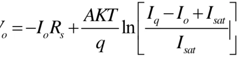
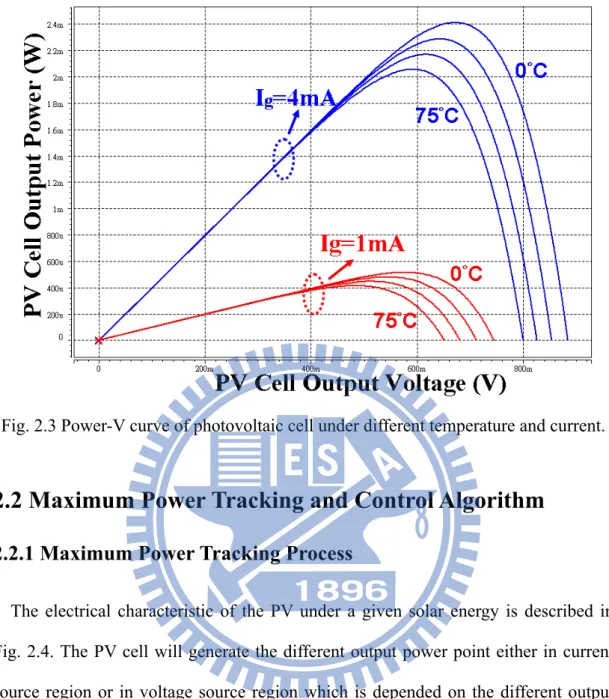
(2.4) As shown in (2.4), the electric power generated by a photovoltaic cell varies with the solar radiation value and temperature. Fig. 2.2 shows the I-V and Power-V curve of PV cell under different temperature at Ig=4mA, and Fig. 2.3 shows the Power-Vcurve of photovoltaic cell under different temperature and current.
Fig. 2.3 Power-V curve of photovoltaic cell under different temperature and current.
2.2 Maximum Power Tracking and Control Algorithm
2.2.1 Maximum Power Tracking Process
The electrical characteristic of the PV under a given solar energy is described in Fig. 2.4. The PV cell will generate the different output power point either in current source region or in voltage source region which is depended on the different output loadings, where the output current or voltage almost maintains as a constant. The intrinsic impedance of the solar array is low on the right side of the current curve and high on the left side of the current curve. The maximum output power of PV cell occurs at the crossing point of the two regions. The power delivered to the load is the maximum value when the source intrinsic impedance matches the load impedance according to the maximum power transfer theory. So, the impedance shown in the converter side should match the intrinsic impedance of the solar array if the system is controlled to operate close to the maximum power region of the photovoltaic cell.
Fig. 2.4 The characteristic curves of PV cell.
In the traditional, most dc/dc converters generate the negative impedance characteristic naturally, through the fact that their current increases when voltage decreases. The behavior is due to the constant input power and the adjustable output voltage of the power supply. If the system generate at the high-impedance (low-voltage) side of the PV cell characteristic curve, the output voltage of PV cell will crash. So, the PV cell is controlled to output at the right side of the curve to perform the tracking process. Otherwise, the converter outputs with the maximum duty cycle, and the output voltage of PV cell is only varied with the given solar energy. Therefore, the system cannot accomplish maximum power tracking and may confuse the present operating point of PV cell for the maximum power point.
Fig.2.5 shows the control flowchart of the maximum power tracking system. When a given perturbation leads to rise in output power of PV cell, the next perturbation is made in the same detection. In this way, the maximum power tracker tracks the maximum power continuously.
Fig. 2.5 The flowchart of MPT control.
2.2.2 Control Algorithms for Maximum Power Tracking
The perturbation and observation method and the incremental conductance method are control algorithms which are often used to achieve the maximum power tracking. Though the incremental conductance method provides good performance under rapidly changing atmospheric conditions, more sensors are needed to execute the measurements for computations and make decision [7]. While the sensors or the system need more conversion time, the computations will produce the larger amount of power loss. On the contrary, while the sampling and execution speed of the perturbation and observation method is faster, then the power loss of the system will be reduced. Besides, this method only requires two sensors, and reduces of hardware requirement and cost.
control [8].
1) Voltage Feedback Control: This method supposes that any fluctuations under the solar energy and temperature of the PV cell are unimportant and that the constant reference voltage is adequate approximation of the true maximum power point. The output voltage of PV cell is used as the control variable for the system. The system maintains the PV cell array operating near its maximum power points by regulating the output voltage of PV cell and matches to a fixed reference value.
The control method is simple, but it has the drawback of neglecting the effect of the solar energy and temperature of the PV cell. This method cannot be widely used to the battery energy storage systems. Hence, the control method is only suitable for using under the constant solar condition, such as a satellite system, because it cannot track the maximum power points of the PV cell when variations in the solar energy and temperature occur.
2) Power Feedback Control: The actual output power of PV cell, for its evaluation from measurements of other quantities, is used as the control variable. Maximum power control can be achieved by forcing the derivative (dP/dV) equal to zero by the power feedback control method. A common approach to the power feedback control is to estimate and maximize the power at the load terminal. However, it maximizes the power to the load, not the power from the PV cell. A converter with MPPT provides high efficiency over a wide range of operating points. The full power may not be supplied to the load completely, due to the power loss for a converter without MPPT. Hence, the design of a high-performance converter with MPPT is a very important issue.
2.3 Ultra Low Voltage Power Management and Computation
Methodology for Energy Harvesting Applications
An ultra low voltage power management system for energy harvesting applications is illustrated in Fig. 2.6[2].
Fig. 2.6 Ultra low voltage power management system for energy harvesting applications.
The ultra low voltage power management system consists of the energy harvesting mechanism, the power management system, the computation module and the charge-based control unit. The environment energy is harvested by the energy harvesting mechanism. The harvested environment energy is transformed into electricity and outputs unregulated voltage.
In this application, the range of output voltage which is harvested from the energy harvesting mechanism is 100mV~200mV. The harvested energy generates unregulated voltage and supply to the source of power management system. There is a charge pump in the power management system. And the charge pump pumps up the voltage to more than 1V for the system. The unregulated voltage (Vs) supplies the controller to let the charge pump is self-powered after it is jump-started. The jump-start circuit is a battery to apply energy during the system is start-up, and be open from the source of the system while the system is self-powered operation. The
unregulated voltage (Vs) supplies the computation unit directly for the cost consideration. Hence the supply voltage fluctuation will impact on the computation unit. The energy is insufficient to maintain continuous computation operation by the impact of the unstable input source energy. The charge-based control unit insures that the energy is sufficient for a step operation of the computation and triggers the calculation operation while enough energy is available.
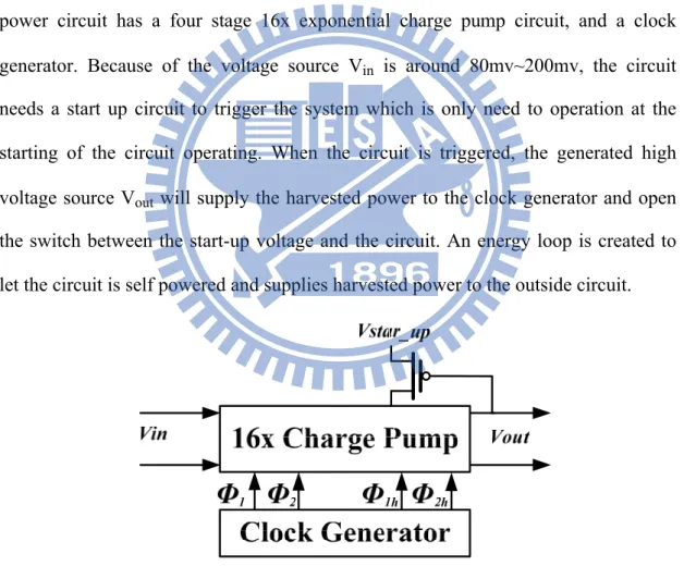
2.3.1 Power Circuit
The power circuit of this power management system shows in Fig. 2.7[2]. The power circuit has a four stage 16x exponential charge pump circuit, and a clock generator. Because of the voltage source Vin is around 80mv~200mv, the circuit
needs a start up circuit to trigger the system which is only need to operation at the starting of the circuit operating. When the circuit is triggered, the generated high voltage source Vout will supply the harvested power to the clock generator and open
the switch between the start-up voltage and the circuit. An energy loop is created to let the circuit is self powered and supplies harvested power to the outside circuit.
Fig. 2.7 Block diagram of the power circuit.
Two different clock phases are used to drive the charge pump: (φ1, φ2) and (φ1h,φ2h). The signal generator shows in Fig. 2.8[2]. For saving energy, all the inverters in the generator for (φ1, φ2) except for the last one of the buffer stage, has to
be swing between Vdd and Vin. The generator for (φ1h,φ2h), the conventional level shifter is removed and a CMOS inverter create a driving signal swing between 2Vout and 4Vin. By doing so, the clock swing is lower and the energy can back to some nodes in the charge pump circuit which can save more energy.
Fig. 2.8 Clock generator.
2.3.2 Computation Module
The unregulated supply voltage impacts the delay of the circuit and will make the timing problem for the operation function. Hence if the computation unit can check the supply voltage variation and adapt the performance of the digital circuit automatically to prevent for the wrong operation will be a good solution. A self-time asynchronous pipeline design [9] is carried out for the computation module. The function of a pipeline stage is only dependent upon the completion of the previous stage, but not reliant the global clock. It is more robust under the voltage variation operation conditions for its previous staged generated timing signals and it is more fitting for the design to track with an unregulated supply voltage. To make easier the
asynchronous hand-shaking protocol and to serve for the static CMOS library, the asynchronous pipeline is implemented by the bundle delay method. The bundle delay is a little bit larger than the computation delay with a safety margin for the voltage variation operation. When the supply voltage is unregulated, the bundle delay will automatically track the change and synchronize the operation in the pipeline. This can tolerant a large variation in the supply voltage.
2.3.3 Charge-Based Control Unit
Because of the variation of the voltage source, sometimes the energy available at a special time interval may be insufficient for a certain operation and if system is running the computation, the computation may be unfinished and the data will be lost when the voltage drops to a lower level. Considering for this situation, a charge-based computation methodology is used. The charge required at different voltage levels for is sure for a certain step operation. The certain step operation refers to a computation which results in data and stores in the memory, or outputs to external device and not to be used again. The certain step operation will only be started when the scavenged power can supply the charge for it with some energy margin. For some ultra low power applications, such as ultra low power wireless sensor device, the computation can operate at a very long clock cycle. The system can make a decision whether an operation could be triggered and executed based on the energy available. Besides, the computation can be prioritized in task level or bit level. Depending on the energy available, different computations will be carried out by depending on the judgment of the charge-based control unit.
2.4 A Micro-Power Management System with Maximum Output
Power Control for Solar Energy Harvesting Applications
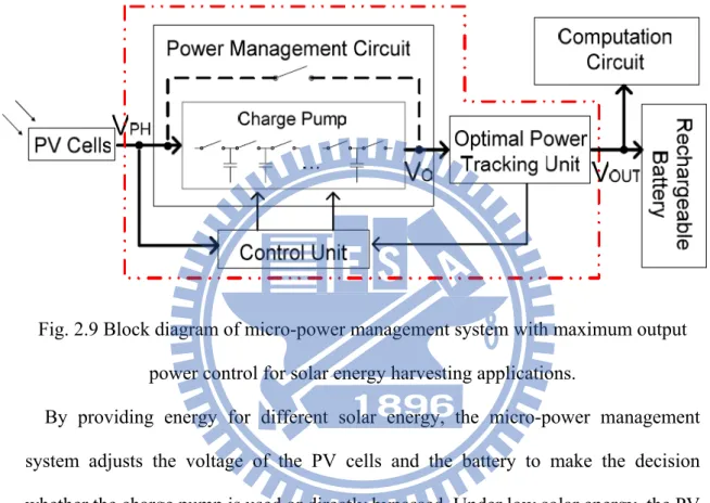
The micro-power management system with maximum output power control for solar energy harvesting applications shows in Fig. 2.9[3].
Fig. 2.9 Block diagram of micro-power management system with maximum output power control for solar energy harvesting applications.
By providing energy for different solar energy, the micro-power management system adjusts the voltage of the PV cells and the battery to make the decision whether the charge pump is used or directly bypassed. Under low solar energy, the PV cell output voltage is low and the charge pump pumps up the voltage either for charging the rechargeable battery or providing energy to the computation circuit. At this moment, the optimal power tracking unit checks the charge pump output power and decides the adjustment of the system operating parameter. Depending on the adjustment decision, the control unit adjusts the operating frequency of the charge pump for maximize the power management system output. Rechargeable battery is used to provide the system continuous energy even while the light source is not sufficient.
2.4.1 Optimal Power Tracking Unit
For supplying maximum power to charge the battery or to directly supply the computation circuit, the optimal power tracking unit is applied to monitor the amount of power flowing out of the charge pump. The detail circuit is shown in Fig. 2.10[3].
The optimal power tracking unit monitors the output power of charge pump and generates the adjustment decision for the decision switching frequency of the charge pump so that make the system is operating around the optimal output power point. The optimal power tracking unit contains the current sensing circuit and the decision generation circuit. Since the system output voltage is regulated by the battery and the voltage of the battery which is equivalent a large capacitor changes the voltage very slowly, therefore, maximizing the output power of the system is match to maximizing the system output current. The circuit utilized current sensor to measure the charge pump output current. Depending on the measured current value, the tracking unit decides whether the system is at the optimal point and supplies the corresponding decision signal to adjust the system parameters. The generic hill climbing algorithm is utilized in the circuit for the optimal point tracking. The switching frequency of charge pump adjusts the system output current. Therefore the tracking unit supplies the corresponding voltage value to adjust the switching frequency by the VCO which is in the control unit. A current sensor consists in the tracking unit. By the biasing current sensed through MN1 and MN2, the source voltages of MP3 and MP4 are
clamped at the same voltage condition. While the current sensor power supply VO is
linked to the charge pump output due to the size ratio of MP1 and MP2, about 1/N of
the total charge pump output current flows to the resistor RS by the transistor MS.
Therefore the output current level from the charge pump is converted by the voltage drop across RS (VS), which is then delivered to the decision generation circuit. The
rest of the charge pump output current would charge the battery or the computation circuit through MP2 at node VOUT. While the output current from the charge pump is
in pulse shape, a smoothing capacitor is connected to the node VO to obtain a smooth
current profile for the accurate measurement of the average value of the output current through the current sensor. The sensed current which is represented by the value of VS,
is delivered to the decision generation circuit to operate the generic hill climbing algorithm. By comparing the current sensed current value with the previous one, the circuit can decide the direction of the change in output current and determine the decision on whether to increase or decrease the charge pump switching frequency. This operation continues and the charge pump output current will oscillate around the maximum current point eventually. In the decision generation circuit, the current detects VS value and the previous VS value is stored in the sample capacitors, CPP1
and CPP2, alternatively. While CPP2 holds the previous value, the transmission gates
circuit T3 and T4 are off while T1 and T2 are on. The current sensed VS will be stored
in CPP1, and Vcheck will output the comparison and detection results from VO+ of the
comparator. Vcheck is equivalent to logic ‘1’ when the current sample value is larger
than the previous sensing value. In the next sample period, T1 and T2 will be turned
off while T3 and T4 are on, and CPP1 holds the previous sample while CPP2 stores the
current VS value. Vcheck will output the comparison and detection results from VO- for
this sample period. This value is XNORed with the previous detection decision which is kept in a D-flipflop and the new adjustment value Vaction will be reset at the rising
edge of the control pulse SE. The logic control value of the decision signal Vaction
determines whether to increase or decrease the charge pump switching frequency. Relying on the Vaction logic value, the capacitor CVCO is either charged by the control
ME4, during the control pulse interval of SE. In this way, the voltage of VVCO is either
increased or decreased and it is then delivered to the control unit to control the charge pump switching frequency through the VCO.
For considering reduce the power overhead, the optimal power tracking unit operation is partition into three different phases during each sample period, which shows in Fig. 2.10. Thus, the sample period demonstrates the time interval between two continuous frequency adjustments. During each period, the transmission gate control signal SPP is either high or low, which decides whether the previous sampled
VS or the current one should be stored in CPP1 or CPP2, and whether VO+ or VO- of the
comparator will output the detection results. Later than each frequency adjustment, the tracking unit is turned off so that all the charge pump output current can flow to VOUT. This describes as the normal working phase. At the end of the normal working
phase, sensor control signal SS will trigger the optimal power tracking unit where the
charge pump output current is sensed and the current changing is checked at node Vcheck. This indicates as the sensing phase. After some delay, the tracking unit goes
into the evaluation phase in which a pulse SE is generated. Decision signal is reset in
the D-flipflop and the capacitor CVCO is charged or discharged through the SE pulse
interval according to the generated decision. After the operation as described before, the power checking unit is turned off and the operation returns back to normal working phase again.
Fig. 2.10 Circuit of the optimal power tracking unit. (①normal working phase, ② sensing phase, ③evaluation phase)
2.4.2 Control Unit
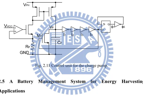
The control unit is utilized to adjust the system operating parameters depend on the determination from the optimal power tracking unit in order to maximize the output power from the charge pump. The charge pump switching frequency has an intense effect on the system output power. A VCO is utilized in the control unit to provide a variable frequency clock. The circuit structure is shown in Fig. 2.11[3]. VVCO is the
output detection signal from the optimal power tracking unit which determines the charge pump switching frequency to be outputted through the inverter chain I1~I4. A
positive edge-triggered D-flipflop resets the clock duty cycle and then delivers the clock signal to the charge pump. For achieving good power transfer efficiency, the
power consumption of the control unit should be minimized. Therefore, the currents of the amplifier branches and the VCO branches should be carefully controlled. Besides, because of VF varies around the threshold of the inverter I1, the short circuit
current of I1 is larger than other inverters. For reducing the current loss, the I1 is
carried out in small size. True Single Phase Clocked (TSPC) register is utilized for the D-flipflop in order to reduce the number of transistors and also its power consumption.
Fig. 2.11 Control unit for the charge pump.
2.5 A Battery Management System for Energy Harvesting
Applications
A battery management system for energy harvesting applications is shown in Fig. 2.12[4] which is contained of RF and thermoelectric. A micro-battery utilized as storage unit and power supply manager to convert and control the harvested energy and interface the micro-battery. Both sources are controlled by the ASICs: the micro-battery being charged either using thermal energy scavenged by the thermo-generator associated with the DC/DC converter or using external RF power transferred by the RF converter. The situation of charge of the storage device is monitored periodically.
Fig. 2.12 The battery management system for energy harvesting applications.
(a) (b) Fig. 2.13 (a) Microbattery electrical model. (b) Normalized state of charge.
2.5.1 Thin-Film Solid-State Battery Electrical Model
The circuit model of micro-battery is shown in Fig. 2.13(a) [4]. The voltage-dependent generator generates the micro-battery voltage which is based on a table. The model has two outputs reproducing the battery state of charge and the
voltage across the battery. The normalized state of micro-battery charge voltage is shown in Fig. 2.13(b) [4].
2.5.2 Micro-battery State of Charge Monitor
The micro-battery state-of-charge monitor is provided energy by the micro-battery itself for ensuring permanent monitoring.The state-of-charge monitor should also be resistant to supply voltage fluctuations to be congenial with the micro-battery. The state-of-charge monitor shows in Fig. 2.14[4]. The monitor detects voltage of battery to a reference voltage and sets the digital soc flag signal to “low” level when the micro-battery is discharged.
Fig. 2.14 Sate of charge monitor architecture.
For achieving ultra low power consumption, the comparator is periodically triggered, only for one second every hour and a half. This sampling rate is enough because of the micro-battery lasts for about one year for the visualized low duty-cycle applications. The comparator is demonstrated in Fig. 2.14[4], as well as the circuit which sends the comparator control signal, and a last circuit which just keeps the comparator output value when the comparator is turned off.
2.5.3 Power Supply Manager and Battery Charger
The micro-battery could be charged by the thermo-generator’s DC/DC output or by the RF converter. Hence, the power supply manager, containing a specific unit along with an asynchronous finite state machine, controls priority between the two sources when they are simultaneously appears and triggers self-powered micro-battery protection avoiding the case of external power source interruption. The micro-battery charge control circuit architecture is demonstrated in Fig. 2.15[4]. The power supply manager provides an internal power supply VDD from the two external sources. This
VDD supply is used by the micro-battery charge controller to provide a constant
current for the micro-battery charge. The power supply manager also generates an internal power supply Vmax defined instantaneously by the maximum voltage between VDD and Vbat. Therefore, this power supply Vmax is steady while using as
small power as possible from the battery. It is used to trigger micro-battery protection avoiding inconveniently discharge in case of external power source interruption.
2.5.4 A Battery Management System to Increase the Service Life of
Battery
From above section description, there are many power management systems for energy harvesting applications which are combined with a rechargeable battery to maintain the overall source power of the system and make the system can work without the harvesting energy source input. The issue of the harvesting power source is that the power source is unregulated voltage source and can not for charging batteries by a constant voltage. Without the control mechanism, the batteries are usually discharged and it is not possible to assure an optimum charge or discharge cycle. The poor charge or discharge cycle may result in reduction of battery life time. A battery management system is used to avoid the battery from repeatedly
overcharged or undercharged. The battery management system is shown in Fig. 2.16[5].
The battery charging method is a very significant factor in extending the life time of the battery in an energy harvesting system. A charge control mechanism is demonstrated in Fig. 2.17[5]. The charge controller has different operation points. The operation points avoid the battery from being overcharged or over-discharged.
1) VR: The voltage regulation operation point limits the maximum voltage that the battery can reach (opens the connection of battery from the array).
2) ARV: The array connects voltage operation point again and gives the voltage at which the battery and array are reconnected.
3) LVD: The low voltage disconnects operation point gives the point at which the battery is disconnected from the load to avoid over-discharged.
4) LRV: The load reconnect voltage operation point gives the voltage at which the load is reconnected to the battery
Fig. 2.16 Battery management system with charge controller.
2.6 Summary
In this chapter, the characteristic of PV cell is defined and its circuit model of PV cell is also described. A maximum power tracking technique is used for PV cell. The MPT controller senses the output voltage and current of PV cell and controls the reference voltage of dc/dc converter to keep the PV cell operating in maximum power. For ultra-low voltage energy scavenging application, a power management system with a small battery for jumping start is described as mention before. The power management system also included a low power clock generator to generate the clock phases for a four stage 16x exponential charge pump circuit. Because of the unpredictable power source and unregulated output voltage, the power management used a charge-base control unit to avoid the computation error.
A charge pump is generally used for solar energy harvesting applications. For efficiency consideration, a micro power management system with maximum output power control is carried out. The system included an optimal power tracking unit to monitor the charge pump output power and made the adjustment decision for the charge pump switching frequency so that the system was working around the optimal output power point.
The battery management system for energy harvesting applications converts the RF power and the thermo-generator power to the micro-battery. The charge monitor is implemented to extend battery operation time and preservation of harvesting energy. The power supply manager detects the usage source is from RF power or from thermo-generator to charge battery. And a battery management system for battery charge method is utilized to avoid overcharged and undercharged for extending the service life time of battery.
Chapter 3 Switched Capacitor DC-DC
Converter and Voltage Regulator
The switched capacitor (SC) DC-DC converter and the voltage regulator are composed of a comparator (or an OP amp.), reference voltage generator (or digital to analog converter for dynamic voltage generation) and an output MOSFET. The ideal voltage regulator is low dropout voltage, low quiescent current, good loading capability and small output transient undershoots and overshoots.
For providing high output current, the transfer MOSFET must be very large. So, the transfer MOSFET will have the large gate capacitor. This will cause stability problem and increase driving power. For archiving high-precision output voltage, a high open loop gain is required. But the phase margin is sacrificed when loop gain is too high and cause regulator unstable. Fast transient response is related to slew rate at the gate drive of the power transistor and the open loop-gain bandwidth. This can be improved by a high slew-rate buffer and advanced frequency compensation technique.
In this Chapter, the techniques of conventional switched capacitor DC-DC converter is explained in Section 3.1, the techniques of improving stability of voltage regulator are illustrated in Section 3.2. A linear regulator using digital buffer is introduced in Section 3.3. The switched capacitor DC-DC converter and voltage regulator is described in Section 3.4. All results are simulated in UMC 90nm CMOS technology model.
3.1 Conventional Switched Capacitor DC-DC Converter
3.1.1 Conventional Structure of Switched Capacitor Matrix
Fig. 3.1 is shown a conventional structure of switched capacitor matrix [42], a multiple-gain DC/DC converter which is used four flying capacitors, CTOP, CMID,
CBOT and CX for delivering charges from the input voltage to convert different output
voltages. And the four flying capacitors are large values, and total size is 2.4nF.
4,6,8,9,12 4,6,8,9,12
V
BATL
L
L
Ф2 Ф1 4CB 4CB 4CB T4 6CB 6CB T6 4CB 4CB 4CB T8 3CB 3CB 3CB 3CB T9 12CB T12 X BOT MID TOP 4CB 4CB 4CB T4 6CB 6CB T6 4CB 4CB 4CB T8 3CB 3CB 3CB 3CB T9 12CB T12 X BOT MID TOPC
TOPC
MIDC
BOTC
X 4,6,8,9,12 4,6,8,9,12 4,6,8,9,12 4,6,8,9,12 4,6,8,9,12 4,6,8,9,12 4,6,8,9,12 4,8,9 4,6,8,9 ALL 4,6,8,9,12Fig. 3.1 Switched capacitor matrix of conventional structure.
The box shown in Fig. 3.1 is representative of a switch which is turned ON depending on the topology in use and the phase of the clock, which are implemented by using N type or P type MOS transistors. The controlling signals of transistor switches are generally using clock signals to control the connections of the flying capacitors by turning on or turning off the transistor switches. When the switch is
energy dissipated in the switch-on resistance, the transistors switches are designed to have a very large ratio of W over L, where W is the gate width and L is the effective gate length. But the very large W makes the dynamic power of control signals increasing and decreases the total conversion efficiency. Therefore, the size of W and the conversion efficiency are trade off.
3.1.2 Conversion Gain Configurations
The operation of switched capacitor matrix is able to provide five different common phases and gain phases, with the gain being the ratio of the output voltage Vout to the input voltage Vin. The equivalent circuits of these conversion phases are
shown in Fig. 3.2 [42].
Fig. 3.2 Topologies used to generate a wide range of load voltages from a 1.2V supply.
In these configurations, there are four gain configurations referred as buck stages whose gains are less than 1 and one gain configuration referred as unit gain with gain equal to 1. According to the input and the output, the DC/DC converter is divided to
step-down type or buck type converter (Vout<Vin).
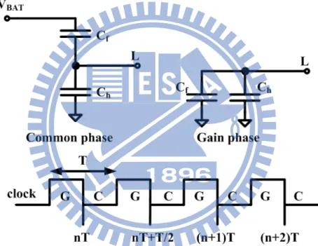
While the converter is clocked and the gain setting is chosen, the switched capacitor matrix is switched between the common phase and the chosen gain phase to transfer charges from the input to the output to keep the chosen output voltage. The gain configuration of 1/2 is used as an example to explain the implementation of gains through the switched capacitor matrix. The equivalent circuit of gain configuration of 1/2 is shown in Fig. 3.3[43] below. The flying capacitor Cf is used to store and
transfer energy, and capacitor Ch is the hold capacitor for the output.
Fig. 3.3 Equivalent circuit of the gain configuration with gain of 1/2.
At time nT, the switched capacitor stays at the end of the gain phase, and the charges in the capacitors Ch and Cf are
(
)
(
)
ch h outQ
nT
=
C V
i
nT
(3.1)(
)
(
)
cf f outQ
nT
=
C V
i
nT
(3.2) At time nT+T/2, the charge pump stays at the end of the common phase, thecharges in the capacitors Ch and Cf are
(
/ 2)
(
/ 2)
ch h outQ
nT
+
T
=
C V
i
nT
+
T
(3.3)(
/ 2)
[
(
/ 2)]
cf f in outQ
nT
+
T
=
C
i
V
−
V
nT
+
T
(3.4)According to the theory of charge conversation, we have
(
/ 2)
(
/ 2)
(
)
(
)
ch cf ch cf
Q
nT
+
T
−
Q
nT
+
T
=
Q
nT
−
Q
nT
(3.5) Solving Equation (3.1) (3.2) (3.3) (3.4) and (3.5) results in(
/ 2)
f h f(
)
out in out h f h fC
C
C
V
nT
T
V
V
nT
C
C
C
C
−
+
=
+
+
+
(3.6)(
)
(
/ 2)
f h f(
)
ch h in h out h f h fC
C
C
Q
nT
T
C
V
C
V
nT
C
C
C
C
−
+
=
+
+
+
i
i
(3.7)(
)
(
/ 2)
f h f(
)
cf h in f out h f h fC
C
C
Q
nT
T
C
V
C
V
nT
C
C
C
C
−
+
=
−
+
+
i
i
(3.8)At time nT+T, the charge pump is switched back to the gain phase. According to the theory of charge conservation, the total charges in the capacitors Ch and Cf are
(
)
(
/ 2)
(
/ 2)
total ch ch
Q
nT
+
T
=
Q
nT
+
T
+
Q
nT
+
T
(3.9) So the output voltage at time nT+T is2 2 2
(
1)
(
)
2
(
)
(
)
(
)
(
)
total out in out h f h f h f in out h f h fQ
V
n
T
aV
bV
nT
C
C
C C
C
C
V
V
nT
C
C
C
C
+
=
=
+
+
−
=
+
+
+
(3.10)According to Equation (3.11), we can have
2
(
2 )
(
)
[
(
)]
(1
)
(
)
out in out in in out in outV
nT
T
aV
bV
nT
T
aV
b aV
bV
nT
a
b V
b V
nT
+
=
+
+
=
+
+
=
+
+
(3.11)2 2 3
(
3 )
(
2 )
[ (1
)
(
)]
(1
)
(
)
out in out in in out in outV
nT
T
aV
bV
nT
T
aV
b a
b V
b V
nT
a
b b V
b V
nT
+
=
+
+
=
+
+
+
=
+ +
+
(3.12)According to Equation (3.12) and (3.13), we can have
2 1
(
)
(1
...
)
(
)
1
(
)
1
k k out in out k k in outV
nT
kT
a
b b
b
V
b V
nT
b
a
V
b V
nT
b
−+
=
+ +
+ +
+
−
=
+
−
(3.13) Where k=0,1,2…. ,because of b<1,we can have2 2 2
lim
(
)
1
2
1
(
)
(
)
2
1
(
)
in out k h f in in h f h f h faV
V
nT
kT
b
C C
V
V
C
C
C
C
C
C
→∞+
=
−
=
=
−
+
−
+
(3.14)3.1.3 Pulse Frequency Modulation (PFM)
Pulse frequency modulation (PFM) or pulse skipping is one of typical methods to be used to regulate voltages in DC/DC converters for high efficiency at light loading. The basic idea is demonstrated in Fig. 3.4.
Fig. 3.4 Waveform of PFM and gain hopping.
While the output voltage Vout is less than the desired voltage Vdesired, the skip signal
is low, and the switched capacitor matrix is clocked to deliver charges constantly to the output. Hence, the output voltage Vout is raised. On the other hand, when Vout is
greater than Vdesired, the skip signal is high, the gate clock of switches is disabled and
the charge pump stays in the common phase. Therefore, there are no more charges to be delivered to the output. Then, Vout is reduced by the load current. Depending on the
switched capacitor matrix’s running or stopping, the converter stays in one of two modes: the deliver mode or the skip mode.
3.2 Stability Scheme of Voltage Regulator
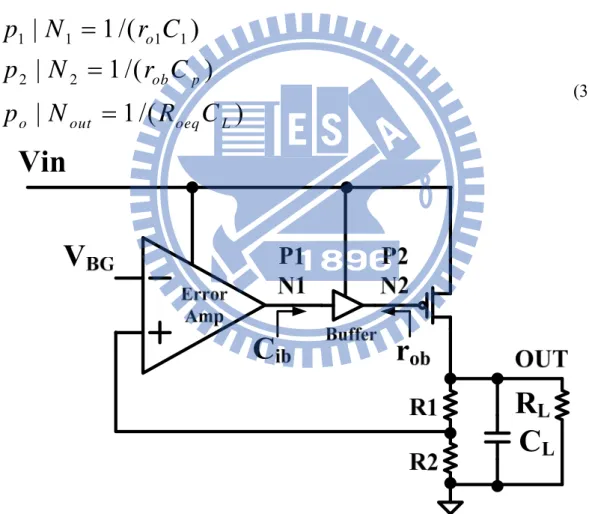
3.2.1 The Dynamic-Biased Shunt Feedback Buffer
A typical structure of a low-dropout regulator shows in Fig. 3.5 which consists of an error amplifier comparing the output voltage to the bandgap voltage Vbg, a PMOS
pass transistor Mp, and the output buffer stage driving Mp. There are three different
poles in the voltage regulator structure located at the output node of the error amplifier (N1), the output node of the buffer (N2), and the output node of the voltage regulator (Vout). In particular, these poles are given by
1 1 1 1 2 2
|
1 /(
)
|
1 /(
)
|
1 /(
)
o ob p o out oeq Lp
N
r C
p
N
r C
p
N
R
C
=
=
=
(3.15)Fig. 3.5 Typical structure of a low-dropout regulator with an intermediate buffer stage. The ro1 is the output resistance of the error amplifier, C1 is the equivalent
capacitance at N1 which is dominated by the input capacitance of the buffer Cib, rob, is
equivalent resistance seen at the output of the voltage regulator. Ideally, both Cib and
rob should be very small in order to achieve single-pole loop response by locating both
p1 and p2 at frequencies much higher than the unity-gain frequency of the regulation
loop.
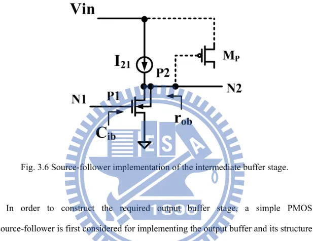
Fig. 3.6 Source-follower implementation of the intermediate buffer stage.
In order to construct the required output buffer stage, a simple PMOS source-follower is first considered for implementing the output buffer and its structure is shown in Fig. 3.6[10]. The PMOS source-follower provides near complete shutdown of the pass device when under the light-load conditions. Because of the output resistance rob of the source-follower is given by 1/gm21, it is necessary to
increase gm21 in order to decrease the value of rob and allow p2 to be located at
frequencies much higher than the unity-gain frequency of the regulation loop. Transconductance gm21 can only be increased either through using a larger W/L ratio
of transistor M21, or through increasing the DC biasing current I21 through M21, or
both. However, increasing I21 would increase the total quiescent current of the
regulator, and the current efficiency of the voltage regulator is degraded. Using a larger W/L ratio of M21 would increase the input capacitance Cib of the buffer, which
is in turn pushes p1 to a lower frequency and the stability would be poorly affected. A
simple PMOS source-follower is, therefore, not a suitable implementation of the output buffer stage in the voltage regulator.
Fig. 3.7 (a) Source-follower with shunt feedback. (b) The buffer with dynamically-biased shunt feedback for output resistance reduction under different
load currents.
For minimizing W/L ratio of M21 and the quiescent current required to reach a
given rob, the source-follower with negative feedback shown in Fig. 3.7(a)[10] is used.
In particular, the npn transistor Q20 is the feedback device connected in parallel to the
output of the source-follower M21 in order to reduce rob through shunt feedback.
When the input voltage at N1 is constant and the output voltage increases, the
magnitude of the drain current of M21 also increases, which in turn increases the base
current of Q20. As a result, the collector current of Q20 increases, reducing the output
resistance rob by increasing the total current that flows into the output node. The
21
1
(1
)
ob mr
g
β
=
+
(3.16) Equation 3.2 shows that the output resistance of the follower is reduced by the current gain β of the shunt feedback device Q20. For example, when an npn transistorwith β more higher then 1 is used, the value of rob would be decreased and the
frequency of p2 at the gate of the pass device is then pushed to a decade higher. As a
result, the quiescent current needed through M21 is greatly reduced to realize gm21 for
a given rob. Similarly, the required transistor size of source-follower M21 is also
reduced. The input capacitance of the buffer Cib is then decreased, which allows p1
given in (3.1) to be located at a higher frequency without dissipating additional quiescent current. It should be noted that the shunt feedback device Q20 can also be
implemented by a NMOS transistor to achieve a similar reduction in the output resistance.
Because of the unit-gain frequency of the regulation loop increases with the load current, the output resistance of the buffer should decrease when the load current increases in order to maintain p2 far away the unit-gain frequency under the entire
load current range. The buffer with dynamically-biased feedback shows in Fig. 3.7(b)[10]. Two PMOS transistors M24 and M25 and the npn transistor Q20 realize
dynamically-biased shunt feedback to decrease rob under different load current
conditions. The output resistance of the buffer is then given by
21 24
1
(1
)
ob m mr
g
β
g
=
+
+
(3.17) The gm24 is the transconductance of the diode-connected transistor M24. As shown inFig. 3.7(b), when the load current flowing through the pass device Mp increases, both
voltages at N1 and N2 decrease. The gate-source voltage of M24 is increased and
that the current through the follower device M21 dynamically increases with the load
current. This boosts the value of gm21, thereby further reducing the output resistance
of the buffer according to (3.3). In addition, the increase in gm24 with the load current
can reduce the value of rob. This effect is significant under heavy load current
conditions. Besides, when the load current increases, part of the dynamically-increased current through M21 flows into the base of Q20 and increases
its collector current. The current gain β of the vertical parasitic npn transistor slightly increases with the collector current, which also helps on reducing the value of rob
when the load current increases.
The dynamically-biased shunt feedback technique reduces both the input and output impedance of the buffer by decreasing the values of Cib and robs. In particular,
the reduction of rob increases with the change of load current. As a result of p2 is
located at sufficiently high frequencies under different load currents, while the voltage regulator only wastes low quiescent current at no-load condition. The benefit of having a smaller C1 by using a smaller size of source-follower device in the buffer
also improves the stability of the voltage regulator.
3.2.2 Zero-Pole Cancellation
A classical CMOS voltage regulator is shown in Fig. 3.8. This voltage regulator is composed of an error amplifier, a voltage buffer, a power PMOS transistor operating in saturation region, a feedback-resistor network and a voltage reference.
The three poles of this voltage regulator are generated at the output of the voltage regulator, the voltage buffer and the error amplifier, as mentioned in Section 3.2.1. The stability of classical voltage regulator based on dominant-pole compensation with pole-zero cancellation as shown in Fig. 3.9. The second pole p2 is cancelled by the
the voltage regulator stability is achieved by locating p3 beyond the unity-gain
frequency of the loop gain for providing sufficient phase margin. However, when loop gain is too high, p3 locates before the unity-gain frequency, and an even larger output
capacitance is required to retain the voltage regulator stability.
Moreover, the power PMOS transistor in the classical voltage regulator must operate in saturation region for considering the stability problem at different input voltages. The change of the voltage gain due to different drain–source voltage is not substantial when the transistor operates in saturation region [12]–[13]. However, if the transistor operates in linear region at dropout, the transistor will operate in saturation region instead as the input voltage increases. As mentioned before, when the loop gain increases, the classical voltage regulator based on dominant-pole compensation may be unstable. Hence, the power PMOS transistor needs to operate in saturation region throughout the entire range of input voltage, so a large transistor size is required for providing a small saturation voltage at the maximum output current.
Freq.
P
3Z
1P
2P
120log|L(jw)|
0dB
pole from output capacitor
pole from error amplifier output
higher loop gain
zero from ESR
pole from buffer output
Fig. 3.9 Loop gain of classical voltage regulator.
3.3 Voltage Regulator with Digital Buffer
The conventional linear regulator is shown in Fig. 3.10[16] and has several limitations. First, the same feedback loop is used for feedback the error signal of VREF
as well as for responding to varying load demand. This problem can be mitigated by using replica biasing with a fast local feedback loop for load regulation. Second, the transient response time depends on the slew rate of the analog buffer to drive the large output device. The slew rate of a class A buffer is directly proportional to the quiescent current which limited the speed of the fast regulator with single stage load regulation. A class AB buffer is more power-efficient but tends to degrade the phase margin of the feedback loop and leads to more aggressive compensation and lower bandwidth.
VREF load Error Amplifier Analog buffer Output device VOUT VIN
Fig. 3.10 Conventional linear regulator topology.
Fig. 3.11 Linear regulator with digital buffer.
The inverters are nearly perfect class AB circuits. They consume little current when idle and provide large output current when switching. As shown in Fig. 3.11[16], the inverters are used as digital buffer. The signal from the error amplifier is first translated by an A/D converter into a thermometer-coded digital output. Digital buffers add drive strength for the A/D converter can quickly turn on and off the parallel legs of the output device. In the steady state, very little current is consumed in driving of the output devices, which eliminates speed-power tradeoff that plagues
traditional class A analog buffers. The schematic of regulator is shown in Fig. 3.12[16].