0925-9635/02/$ - see front matter䊚 2002 Elsevier Science B.V. All rights reserved. PII: S 0 9 2 5 - 9 6 3 5 Ž 0 1 . 0 0 6 6 1 - 6
Abstract
In this study, we used methaneycarbon dioxide gas mixtures to deposit nanoemitters on the gate-structured metal–insulator–
semiconductor(MIS) diodes. Due to the nanoemitters growing in a high carbon concentration gas source of CH yCO , the growth4 2
rate is better than conventional mixtures by using hydrocarbons diluted in hydrogen. Moreover, the bias also promotes the growth rate in the CH4yCO gas mixtures. In addition, selected area deposition2 (SAD) of emitters was successfully achieved by using
the Pt layer as inhibitor in the bias assisted microwave plasma chemical vapor deposition (BAMPCVD). The field emission
current and the current density of nanoemitters on field emission arrays (FEAs) are 154 mA and 490 mA cm , respectively.y2
This may be due to the following reasons:(I) short gate-emitter spacing; (II) small gate aperture; and (III) emitter with a sharp
feature.䊚 2002 Elsevier Science B.V. All rights reserved. Keywords: Field emission; CVD; SEM; Raman spectroscopy
1. Introduction
The emission of electrons from the surface of diamond and diamond-like carbon (DLC) films has attracted
much attention due to its potential application in cold cathode devices. Diamond possesses negative electron affinity(NEA), in addition to remarkable characteristics such as large thermal conductivity and being chemically inert. Many studies have focused on fabricating diamond films w1x or diamond-clad silicon field emission arrays
(FEAs) w2x.
The most popular gas mixtures for the chemical vapor deposition (CVD) of diamond are hydrocarbon diluted in hydrogen. Therefore, hydrogen is a very high per-centage in the gas mixtures and the diluted hydrocarbon gas is the only source of carbon. In this study, we used methaneycarbon dioxide to deposit carbon nanoemitters
in triode-type FEAs without hydrogen dilution. Further-more, the selective area deposition (SAD) of
nanoem-*Corresponding author. Tel.: q886-9-3588-9532; fax: q886-6-261-6193.
E-mail address: [email protected](C.L. Tsai), [email protected](C.L. Tsai).
itters by using a Pt layer as a nucleation inhibitor is also successfully completed in the CVD process.
2. Experiment
The fabrication process of the metal–insulator–semi-conductor (MIS) diode and diamond-like deposition
procedure have been previously presented w3x. First, we made the MIS diode structure by semiconductor process technology. Starting substrates were mirror-polish n-type,
(100) oriented wafers with a resistivity of 4.5;5.5 V
cmy1. After fabricating the MIS diode, specimens were put in the bias assisted microwave plasma chemical vapor deposition (BAMPCVD) system to deposit dia-mond with various deposition parameters. Fig. 1 shows the cross-section of the triode-type structure. The reac-tive gases used in deposition were the mixtures of CH –4
CO . The flow rates of CH2 4yCO and deposition time2
remained constant at 30y30 sccm and 15 min,
respec-tively. While processing the deposition, the specimens were subjected to a negative bias voltage. Table 1 lists the experimental conditions.
Scanning electron microscopy (SEM) was used to
Fig. 1. The schematic cross-section of a triode device structure.
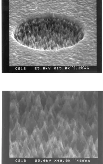
Fig. 3. SEM photograph of sample B growing under 130 V.
Fig. 2. SEM photograph of sample A growing under 120 V.
Table 1
Deposition conditions of nanoemitter
Sample Flow rate CH4yCO2 Negative bias Deposition time
(sccm) (V) (min)
A 30y30 120 15
B 30y30 130 15
C 30y30 150 15
D 30y30 180 15
Total pressures15 torr; microwave powers300 W; Substrate temp. f750 8C.
micro-Raman spectroscopy was used to identify the quality of emitters, and an I–V measuring system to
obtain their field emission characterization. The field emission properties of the FEAs were measured by using a triode technique. An anode plate, an ITO glass,
was placed at 100 mm above the Pt-gate and was biased to q800 V. The anode current (I ) was then measuredA
as a function of gate-to-cathode bias voltage in a vacuum of 1=10y6 torr. The gate-to-cathode voltage(V ) was
gc
biased from 0 to 50 V. During testing, the device was in a common emitter configuration and both the anode and gate being positive potentials to turn the device on.
Fig. 4. SEM photograph of sample C growing under 150 V. Fig. 5. SEM photograph of sample D growing under 180 V.
Fig. 6. Raman spectra of nanoemitters growing under different applied bias.
3. Results and discussion
Figs. 2–5 show SEM photographs of nanoemitters growing under different bias. Each picture is only one of the 50=50 circles on the FEAs. Every picture in the bottom side is an enlarged image of the top one. The width and the depth of the hole are 4 mm and 7000 A,˚ respectively. Under the bias below 130 V, there is only low density of tiny tips inside the hole. Fig. 2 shows a SEM photograph of the nanoemitters growing under 120 V. Once we increased the deposition time, which is over 15 min, not only inside the hole but also on the Pt-gate were carbon materials. Indeed, the carbon materials may replace the Pt to form the carbon-gated FEAs. In the worst case scenario, this phenomenon will taint the I– V measurement because the field emission current
may-be inexact may-because of the influence from both the nanoemitters and carbon-gated surface. Figs. 4 and 5 display that higher bias drastically enhances the growth
Fig. 7.(a) The emission current (I ) vs. the gate voltage (V ) anda gc
(b) the emission current density (J ) of nanoemitters growing undere
130 V on FEAs.
Fig. 8. TheF–N plot of nanoemitters growing under 130 V on FEAs.
rate of nanoemitters. However, this leads the triode-type device to a diode structure because of the emitters exceeding the height of the hole.
Examining Figs. 2–5, we get the following results.
(I) The applied bias can enhance the growth rate of
nanoemitters with CH4yCO gas mixtures in CVD proc-2
ess. Moreover, the higher bias is applied, the higher growth rate is obtained. The bias effect is also valid for the hydrocarbon diluted in hydrogen w4x.(II) The growth
rate of CH4yCO gas mixtures is better than the con-2
ventional gas CH4yH w5x. This is due to the nanoem-2
itters growing in a high carbon concentration gas source of CH4yCO .2 (III) In addition, the deposition under
high bias will cause higher density, larger and sharper nanoemitters. Thus, emitters with sharp features have small radius curvature and high aspect ratio. (IV) All the emitters directly grow upward under bias condition.
The region for diamond growth is indicated in the C–H–O diagram presented by Bachmann et al. w6x. The parameter range for diamond deposition from CH4y
CO is narrower than the CH2 4yH . The molar ratio of2
CH4yCO s1.08;1.63 is needed for diamond growth.2
In terms of the ratio of CyO, the range is from 1.04 to ;1.31. When the ratio is out of this range, the graphite
is found on the deposit. In other words, the growth conditions are very restrictive. Nevertheless, due to the difference of various deposition conditions such as microwave power, pressure and substrates, etc., the results maybe change. In this study, the volume ratio of CH4yCO s1 is used.2
Fig. 6 shows Raman spectra of emitters growing under applied various bias. We find there is no obvious difference among these spectra. All of them have two sharp peaks located at approximately 1355 cmy1 and 1582 cmy1, respectively. These imply that the nanoem-itters are characteristic of microcrystalline graphite. The Raman spectra of amorphous carbon can be decomposed into two features located approximately at 1550 cmy1 (corresponding to the G-line associated with the
opti-cally allowedE2gzone center mode of crystalline graph-ite) and 1350 cmy1(roughly corresponding to the D-line
associated with disorder-allowed zone-edge modes of graphite). The positions, widths, and relative intensities
of these two peaks are found to vary systematically with deposition conditions and emitters’ properties w7,8x. The intensity of these two peaks is the same. This indicates that there is much amorphous carbon in the samples.
Fig. 7 displays the electron-emitting characteristic of the nanoemitters growing under 130 V on FEAs. If the applied bias is above 130 V, the emitters will grow over the hole. This indicates that the emitters exceed the height of Pt-gate. Under this condition, the device becomes diode structure instead of triode-type one. The field emission current (I ) of nanoemitters from all ofa
gate-rapidly as tip radius and gate aperture decrease w11– 13x.
The threshold voltage(V ) is defined as the intersec-th
tion of the F–N plots shown in Fig. 8 with the abscissa.
The threshold voltage (V ) is approximately 13 V forth
the nanoemitters. Due to the smaller gate aperture; diameter and shallower gate structure, a field emission can be triggered at a lower threshold voltage. However, there is a saturated current atV s50 V for nanoemittersgc
on FEAs. This phenomenon is caused by the fact that the dielectric layer(SiO ) in the developed pattern may2
be broken under high applied voltage, which will create a leakage current.
4. Conclusions
In this study, we successfully fabricated the triode-type FEAs for decreasing the turn-on voltage and increasing the emission current. Results are summarized as follows.
1. First, we successfully completed the selective area deposition(SAD) of nanoemitters by using a Pt-layer as a nucleation inhibitor in the BAMPCVD process. 2. Due to the nanoemitters growing in a high carbon
concentration gas source of CH4yCO , the growth2
References
w1x A. Watanabe, M. Deguchi, M. Kitabatake, Diamond Relat. Mater. 10(2001) 818.
w2x N.J. She, A Study of Application and Characterization of Diamond Thin Films on Field Emitter Arrays, Master’s Thesis, Chiao Tung University, 1996.
w3x C.F. Chen, H.C. Wang, H.C. Hsieh, Jpn. J. Appl. Phys. 39 (2000) 1880–1884.
w4x S. Yugo, T. Kanai, T. Kimura, T. Muto, Appl. Phys. Lett. 58 (1991) 1036.
w5x C.-F. Chen, H.-c. Hsieh, Diamond Relat. Mater 9(2000) 1257. w6x P.K. Bachmann, D. Leers, H. Lydtin, Diamond Relat. Mater. 1
(1991) 1.
w7x M.A. Tamor, W.C. Vassell, J. Appl. Phys 76(6) (1996) 3823. w8x J. Wagner, M. Ramsteiner, Ch. Wild, P. Koidl, Phys. Rev. B
40(1989) 1817.
w9x J.M. Kim, Process Technology and Characterization for Field Emission Devices, Michigan UMI, 1992, p. 10.
w10x D. Temple, Mater. Sci. Eng. R 24(1999) 191.
w11x R.B. Marcus, K.K. Chin, Y. Yuan, H. Wang, W.N. Carr, IEEE Trans. Electron Dev. 37(1990) 1545.
w12x J.H. Kang, J.W. Cho, J.W. Kim, J.M. Kim, J.Vac. Sci. Technol. B14(1996) 1924.
w13x E.G. Zaidman, K.L. Jensen, M.A. Kodis, J. Vac. Sci. Technol. B 14(1996) 1994.