全球定位系統專用低功率整數N頻率合成器
72
0
0
全文
(2) 全球定位系統專用低功率整數 N 頻率合成器 A Low Power Integer-N Frequency Synthesizer for Global Position System 研究生:汪揚. Student:Yaung Wang. 指導教授:高銘盛、周復芳. 博士. Advisor Dr. M. –S. Kao , Dr. Christina F. Jou. 國立交通大學 電信工程學系碩士班 碩 士 論 文 A Thesis Submitted to Department of Communication engineering College of Electrical Engineering and Computer Science National Chiao Tung University In Partial Fulfillment of the Requirements For the Degree of Master of Science In Communication Engineering June 2003 Hsin Chu, Taiwan, Republic of China. 中 華 民 國 九 十 三 年 七 月.
(3) 全球定位系統專用低功率整數 N 頻率合成器 研究生:汪揚. 指導教授:高銘盛、周復芳 博士. 國立交通大學 電信工程學系 碩士班. 摘要 本論文中提出一全球定位系統專用的頻率合成器,其工作頻率在 1.57GHz, 為了達到低功率損耗的目的,我們將操作電壓設定在 1.5 伏特,且除頻器部份考 慮降低電流使用量,採用較省電的整數 N 組態,所有電路除迴路濾波器及參考 振盪器外,均製作在同一晶片上以達高整合目的,晶片製作則是採用台積電 CMOS 0.25um 製程。 在 1.5 伏特的電壓供應下,所量測到的功率損耗為 14.1 毫瓦。壓控振盪器消 耗 6.8 毫瓦,除頻器消耗 6.6 毫瓦,充電幫浦消耗 0.64 毫瓦,相位/頻率比較器消 耗不到 1 毫瓦。. I.
(4) A Low Power Integer-N Frequency Synthesizer for Global Position System. Student: Yaung Wang. Adviser:Dr. M. –S. Kao , Dr. Christina F. Jou. Institute of Communication National Chiao Tung University Abstract In this thesis, we demonstrate a low power synthesizer for global position system (GPS) which operates at 1.57GHz. For low power consumption consideration, we set the supply voltage at 1.5V, and adopt the “Integer-N” type frequency synthesizer to save power. For high integration issue, all circuits are integrated in single chip except the loop filter and the reference oscillator. This chip is fabricated by TSMC 0.25um. The measurement of power consumption is 14.1mW for 1.5V supply voltage. VCO consumes 6.8mW, frequency divider consumes 6.6mW, charge pump consumes 0.64mW, and phase/frequency detector consumes less than 1mW.. II.
(5) 誌 謝 首先要感謝高銘盛老師在兩年中給我不斷的鼓勵與指導,不單在專業上使我 學會該如何處理問題,在心理方面也有相當大的成長,您對學生親切的態度更化 解了和師生間的那道牆,打破往只建立在學業上的師生關係,而周復芳老師總是 適時給我們關心,您獨特的美式做風及親和力十足的談吐讓我們能有一個最快樂 的學習環境,國華學長對實驗室的同學也給予最大的協助,給我們最豐富的學習 資源及科技資訊。 接著要感謝朝安、先承、邦瑞學長常在困惑時提供自己的經驗供我參考,讓 我順利解決碰到的問題,雖然和你們只有短短一年的相處,卻是學習生涯中最豐 富的一段時光,你們的出現也讓我多了幾位一生的摯友,另外感謝蕭旭風學長給 我量測上最大的協助,沒有你們,我的論文無法進行的如此順利。 同窗兩年的同學們更是讓我無法忘記,蒼哥豐富的人生閱歷讓不但讓大家增 添不少見聞,你對任何事物的投入態度更讓我看到自己不足的地方,另外炳宏的 熱心助人及開朗笑容讓實驗室多了份歡樂,也更添溫暖,政良的友善態度及豐沛 的專業知識讓我在學習上更為順利,政宏、家良、欽賢、偉程、柏達及俊賢對實 驗室的付出也是不遺餘力,讓身為碩二的我們,能全力投入在論文研究上。 最後要感謝兩年來陪我一起走過的朋友們,Jack、angus、彥宇、怡中、emi、 stephanie、lena、susie、jasmine 等諸多好友,你們在這兩年中帶給我的快樂 與鼓勵不但豐富了我的人生,更讓我成長許多,沒有你們,這兩年的生活不會如 此多姿多采,另外要特別感謝"Q",讓我碩士最後這一年中能擁有二十三年來最 美好的回憶,所有的感謝都在心裡,藉著短短的文字讓你們知道,希望你們感受 到我由衷的謝意,更願未來的人生道路上能有你們繼續陪伴。. III.
(6) CONTENTS CHINESE ABSTRACT………………………………………….……..I ENGLISH ABSTRACT………………………………….……………II ACKNOWLEDGMENT…………………………………..…………III CONTENTS…………………………………………………………..IV TABLE CAPTIONS……………………………………….………….VI FIGURE CAPTIONS………………………………………………..VII. Chapter 1 INTRODUCTION……………………….………..…….1 1.1 GPS background and motivation………………….…………………….1 1.2 Typical GPS frond end receiver architecture………..…………….....3 1.3 Other reference works……….……………….……………………4 1.4 Thesis organization….……………….…………………….……………6. Chapter 2 PLL THEORY AND NOISE IN PLL LOOPS ...........7 2.1 Basic PLL theory……………………..……………………………………7 2.2 Noise in PLL loops……………………………………………………14. Chapter 3 FREQUENCY SYNTHESIZER………………………17 3.1 VCO design……………………………………………………………..18 3.1.1 Complementary & all-NMOS couple pair VCO………………18 3.1.2 Design for low power and low phase noise……………………21 3.1.3. Architecture and simulation……………………………………23. 3.2 Frequency divider design………………………………………………28 3.3 Phase/Frequency detector design……………………………32 3.4 Charge pump design………………………………….……………34 IV.
(7) 3.4.1. Single-ended & differential charge pump……….……………34. 3.4.2. Architecture and simulation……….…………………….……..35. 3.5 Loop filter design………………………………………….……………37 3.6 Complete loop simulation & layout…………….…………………38. Chapter 4 MEASUREMENT RESULTS………………………….40 4.1 VCO measurement………….…………………………………………41 4.1.1. What is the problem with varactor……….…………………….42. 4.2 Frequency divider measurement………………………………………44 4.3 PFD and charge pump measurement………………..………………52 4.4 Discussion……………..…………………….….………………………55. Chapter 5 CONCLUSIONS AND FUTURE PROSPECTS…….57 5.1 Conclusions……………………………………………………………57 5.2 Future prospects………………………………………………………58. REFERENCES………………………………………………………59 PUBLICATION REMARKS……………...………………………….61. V.
(8) TABLE CAPTIONS Table. 1. Specification summary of the first reference…………………4. Table. 2. Specification summary of the second reference………..………5. Table. 3. Specification summary of the third reference……….……………6. Table. 4. Low-power & low-phase noise optimization summary………23. Table. 5. VCO specification summary………………………………………28. Table. 6. Power consumption summary……………………………………55. VI.
(9) FIGURE CAPTIONS Fig. 1. GPS signal……………………………………………………………….2. Fig. 2. GPS front end receiver………………………………..…………………3. Fig. 3. Third-order PLL linear model…………………………………………9. Fig. 4. Second-order loop filter…………………………………………………9. Fig. 5. Transfer function of Z(s)…………. ….………………………………10. Fig. 6. Frequency response of | G ( s ) |, | H ( s) | ………………………………11. Fig. 7. The effect of third pole in step response………………………………13. Fig. 8. Interrelation with each pole and zero…………………………..……13. Fig. 9. The linear PLL model with noise added……………………………...14. Fig. 10 Phase noise contributions in a PLL……...……………………………16 Fig. 11 “Integer-N” PLL architecture…………………………………………18 Fig. 12 Two typical LC-tank oscillator structures………………………….…19 Fig. 13. Phase noise simulation results for both structures……………...….20. Fig. 14 Basic LC resonator tank………………………………………………21 Fig. 15 VCO architecture with bank sets and output buffer. Vctrl …………24. Fig. 16 The measured phase noise vs. VDD and Isupply for complementary LC oscillator…………………………………………………………………..25 Fig. 17 VCO transient simulation……………………………………...……26 Fig. 18 VCO FFT simulation……………………………………….……………26 Fig. 19 VCO tuning range simulation……………………………………..…27 Fig. 20 VCO phase noise simulation……………………………………..…27 Fig. 21 Frequency divider architecture………………………..………………29 Fig. 22 Block diagram of a master-slave D-flipflop…………………………29 VII.
(10) Fig. 23 SCL D-latch structure…………………………………….…………30 Fig. 24 Differential Source Coupled Logic……………………. ………………31 Fig. 25 VCO& Frequency divider simulation result……………..…………32 Fig. 26 Phase/Frequency detector architecture………………………………32 Fig. 27. f ref is faster than f div and upp is set……………………..…………33. Fig. 28. f div is faster than f ref and dwp is set……………………….………34. Fig. 29 Single-ended charge pump with switch at drain ………….…………35 Fig. 30 Differential charge pump architecture…………………………………36 Fig. 31 The simulation of Icp when upp and dwp are set…………………37 Fig. 32 Passive loop filter architecture…………………………………………37 Fig. 33 Settling time simulation with fix channel……………..………………38 Fig. 34 Settling time simulation when sweeping channel…….……………39 Fig. 35 Layout of the synthesizer……………..…..…..………………………39 Fig. 36 Die photo…………….…..…..…..…...…..…..….………………………40 Fig. 37 All measurable points of VCO…………..…..……..………………….42 Fig. 38 PCB of frequency divider measurement……………..……………….44 Fig. 39 Photograph of instruments …………………………….………………45 Fig. 40 Probe pad photo …………………….…………...…………...…………46 Fig. 41 Probe pad diagram……………………………………………………47 Fig. 42 First stage sets to divide-by-2 model…………….…………………….48 Fig. 43 First stage sets to divide-by-3 model…………………………………48 Fig. 44 Only the first stage is set to divide-by-3 model….…………………49 Fig. 45 Both of the first and the second stage are set to divide-by-3 model……………………………………………………………..………50 Fig. 46 Output spectrum when divide-by-1536…..…….……………..………51 VIII.
(11) Fig. 47 Output spectrum when divide-by-1575………………..……………51 Fig. 48 The spectrum of the reference oscillator……………………..………52 Fig. 49. f div is higher than f ref , Vctrl is pulled down to 0V……..……………53. Fig. 50. f div is lower than f ref , Vctrl is pulled up to 1.5V……………………54. Fig. 51 Loop diagram with external VCO…….….….……………..…………56. IX.
(12) Chapter 1 INTRODUCTION. 1.1 GPS Background and Motivation Applications and developments of wireless communication had grown rapidly during the past decade. Radio frequency integrated circuit (RFIC) is the hottest subject in the academic community and industry, most of the researches are focused on low cost, low power consumption and high integration. Various functions have been launched and applied in new products, for example, global position system (GPS) is widely used in navigation and driving, whereas many cars, cell phones and PDA are equipped with it.. GPS was developed by the United States Department of Defense (DOD), primarily for military purpose. However, the most significant developments over the last 10 to 15 years had all come from the civilian sector. There are four satellites in the space, which can provide a 3-dimensional environment (the fourth satellite can model the time offset between ‘GPS time’ and receiver clock). By measuring the time difference received from each satellite, after computing, we can decide its position accurately.. The GPS satellites broadcast signals in two bands: the L1 band, which is. 1.
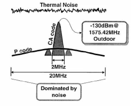
(13) centered at 1.57542GHz, and the L2 band, centered at 1.2276GHz. Each satellite broadcasts two different direct-sequence spread-spectrum signals. They are known as the P code (precise code) and the C/A (Coarse/Acquisition) code. P code is broadcast in both frequency bands for military use, and C/A code is broadcast only in L1 (1.57542GHz) band for commercial use (Fig. 1). Bit rate of C/A code is 50-b/s spread over 2MHz bandwidth. Received signal power is around -130dBm and power spectrum density (PSD) is about -193dBm/Hz lower than the thermal noise level [1]. And GPS front end downcoverter. chips. produced. by. Valence. semiconductor. have. the. specification about phase noise; -70dBc/Hz@10KHz and -105dBc/Hz@1MHz. . Fig. 1 GPS signal. 1.2 Typical GPS frond end receiver architecture 2.
(14) A typical GPS frond end receiver being designed for L1 band and C/A code is illustrated in Fig. 2. This receiver incorporates a fully integrated LNA front-end, IF section and a frequency synthesizer whose loop filter and reference oscillator are off chip.. An active antenna receives the GPS signal from satellites. After matching circuit the signal is sent to the LNA, the low-noise mixer and is down converted to a quadrature IF of 1.023MHz. The filters follow the mixers are used for the channel selection. Then, the signal passes through a fifth-order complex elliptic filter that rejects the image noise by an average of 18dB. A chain of variable gain amplifier (VGA) provides gain for IF signal before sending to the comparator (COMP).. Fig. 2. 1.3. GPS front end receiver. Other Reference Works 3.
(15) From above we know the architecture of the whole front end receiver, next we review some references to realize the specification of other synthesizer works.. 1. The measurement result of the synthesizer in the first reference “A Fully Integrated Low-IF CMOS GPS Radio With On-Chip Analog Image Rejection” [2] is shown below:. PLL spurs. -63dB. VCO phase noise @ 1MHz offset. -107dBc/Hz. PLL In-band phase noise with 70KHz -72dBc/Hz. PLL bandwidth. Settling time. <5ms. Power consumption (whole chip). 27mW. Table. 1. Specification summary of the first reference. 2. In the second reference “A 35-mW 3.6mm 2 Fully Integrated 0.18-um CMOS GPS Radio” [3], the measurement result of the synthesizer is shown below:. 4.
(16) PLL spurs. <-35dB. VCO phase noise @1MHz offset. -95dBc/Hz. Settling time. <1ms. Power consumption. 16.7mW. Table. 2. Specification summary of the second reference. 3. A data sheet “A GPS front end downconverter”[4] produced by Valence semiconductor has the specification about synthesizer.. PLL spurs. -70dB. VCO phase noise @1MHz offset. -105dBc/Hz. Charge pump current (Icp). 0.5mA. KVCO. 220MHz/V. Table. 3. Specification summary of the third reference 5.
(17) 1.4 Thesis Organization In this thesis, we bring up a complete design flow, circuit architecture, simulations, layout and measurement of a low power GPS frequency synthesizer fabricated by TSMC 0.25um technology. Here is the organization of this thesis.. In Chapter 2, a simple PLL design theory will be introduced with special consideration of the often- seen noise effect in VCO and PLL.. In Chapter 3, we build up the architecture of our synthesizer and compare with other structures. Then we simulate the synthesizer performance and draw the layout.. In Chapter 4, measurement results of the fabricated synthesizer will be presented.. In Chapter 5, we discuss the measurement results and then make the conclusion. We further present future prospects to achieve better performance.. 6.
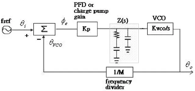
(18) Chapter 2 PLL THEORY AND NOISE IN PLL LOOPS Phase-locked loop (PLL) is the critical part in modern communication systems. It can be used as an oscillator to generate various frequencies for up/down conversion in super-heterodyne transceivers. It can also be used to regenerate the carrier from an input signal in which the carrier has been suppressed. On concerning PLL performance, two noise sources, i.e., VCO phase noise and input noise, play the critical role in the noise performance. In this chapter, we will first introduce simple PLL theory and then discuss the relationship between noise and system performance.. 2.1 Basic PLL Theory The purpose of PLL is making one tunable frequency lock to a reference frequency via a feedback loop. Basic PLL architecture consists of a voltage controlled oscillator (VCO), a frequency divider, a phase/frequency detector. 7.
(19) (PFD) and a loop filter (LPF). Although both PFD and VCO may be highly nonlinear, we still assume linearity when loop is under lock.. On analyzing PLL, loop filter is closely related to PLL behavior such as stability, settling time, bandwidth, and noise performance. Thus we focus on it. There are two kinds of loop filter - passive and active loop filters. Based on some reasons we use passive elements (R, L, and C) as our loop filter rather than active elements (OP amp). First, passive elements are much cheaper and simpler than active ones. Second, for passive filter, maximum DC gain is unity, whereas active loop filter can provide very high DC gain (almost infinity); we don’t need such a high DC gain to push Vctrl to achieve wide tuning range in the wireless communications. Third, passive loop filter consumes less power than active loop filter. Thus we build the loop filter by passive elements.. Based on the order of LPF, it can be classified as the first, the second, the third and the fourth-order PLL. In the first-order PLL, the steady state phase error φe =. f ref BW. , and the loop bandwidth ( BW ) is always much smaller. than the reference frequency ( f ref ) in PLL design, therefore, the steady state phase error is very large. In order to force the steady state phase error to zero, the second-order PLL is introduced. But the settling time of a second-order PLL is more than twice as much as the first-order PLL, and the spurious noise problem is still serious [5]. So we added one capacitor to increase the PLL order to three which is shown below. This is also the loop filter I chosen in my thesis. The third-order PLL linear model with passive loop filter is illustrated in Fig. 3.. 8.
(20) Fig. 3. Third-order PLL linear model. The loop filter of the third-order PLL is shown in Fig. 4. We first derive its impedance transfer function. Fig. 4. Second-order loop filter. 9.
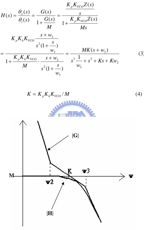
(21) Z (s) =. 1 1 1 + sC1 R1 //( R1 + )= sC2 sC1 s[sC1C2 R1 + (C1 + C2 )]. 1 ) s + w2 C1R1 = = Kh s s (C1 + C2 ) s ( + 1) s ( + 1) C1 + C2 w3 C1C2 R1 C1R1 ( s +. Thus, K h =. (1). 1 C C + C2 C1R1 , w2 = , w3 = 1 = w2 ⋅ (1 + 1 ) (C1 + C2 ) C2 C1C2 R1 R1C1. And the response of | Z ( s ) | is shown below:. Fig. 5 Transfer function of Z(s). The forward gain of the loop is given as:. G (s) =. where K p =. Ip 2π. K p Z ( s) KVCO s. = K p K h KVCO. in charge pumped PLL. 10. s + w2 , 2 s s ( + 1) w3. (2).
(22) Thus the whole loop transfer function H (s ) is given below and the response of H (s ) is shown in Fig. 6.. K p KVCO Z ( s ). H ( s) =. G (s) θ o ( s) s = = K K G s ( ) θi ( s) 1 + p VCO Z ( s ) 1+. M Ms s + w2 K p K h KVCO s s 2 (1 + ) MK ( s + w2 ) w3 = = 1 K p K h KVCO s + w2 s3 + s 2 + Ks + Kw2 1+ ⋅ s w3 M s 2 (1 + ) w3 K = K p K h KVCO / M. (3). (4). |G|. M. |H|. Fig. 6 Frequency response of | G ( s ) |, | H ( s ) |. Now we discuss the bandwidth of PLL. For low w , | H ( S ) |≈ M ; for w2 ≤ w ≤ w3 ,. 11.
(23) | Z ( s) |≈ K h . Let | H ( s ) |=. M when w = w3dB and assume w2 ≤ w3dB ≤ w3 , we 2. can solve Eq. (3) and get the 3dB bandwidth of | H ( s ) | as :. w3dB =. K p K h K vco M. =K. (5). This result for the bandwidth is valid when w > w2 , | Z ( s ) |≈ K h , and we get. w3dB = K .Therefore, we require that w2 < K. (6). On concerning PLL step response we know that the higher of the ratio. w2 we K. set, the larger damping and longer settling time we get, thereby a good rule of choosing the value of w2 is:. w2 =. K. (7). 4. Next we focus on the design of the other pole w3 . The noise out of w3dB will attenuate very quickly and add w3 will suppress the high-frequency component (jitter). If w3 > K , PLL bandwidth is still the same. But the noise rejection capability will decrease if w3 is too far away from K . There is still a good rule to choose the value of w3 :. w3 = 4 K. (8). The only disadvantage to add this pole is that the overshoot will increase to 18% (compares with 13% for the case w3 = ∞ illustrated in Fig. 7). 12.
(24) Fig. 7 The effect of third pole in step response. As we discuss Z ( s) , w2 and w3 , there is an interrelation between each pole and zero. W. >x4. >x4. >x10. Pole Zero= w2. PLL Bandwidth. Extra pole. w3. Reference Clock f ref. Fig. 8 Interrelation with each pole and zero. According to this interrelation, we can determine the location of each pole and zero. Then by Eq. (1) we can derive the R, C value of loop filter.. 13.
(25) C + C2 KN 1 1 ) = K h (1 + ) = (1 + ) R1 = K h ( 1 C1 X K p KVCO X 1 C1 = w2 R1 C2 = C1 X where X =. C1 is the ratio of C1 and C2 C2. 2.2 Noise In PLL Loops There are several noise sources in a PLL. The three main noise sources are that of the VCO phase noise. φnv , noise of the reference signal φni. the noise due to the phase detector. and. φnd . Fig. 9 shows the linear PLL model. with these three noise sources added.. Fig. 9. The linear PLL model with noise added. We begin to discuss the influence caused by each noise. We derive the. 14.
(26) output phase noise. φo. due to each noise source respectively and add them. afterwards. The result is written as :. φo =. (φni + φnd ) K p K vco F ( s ) / s. The first term of. 1 + K p K vco / Ms. φo. +. φnv 1 + K p K vco F ( s ) / Ms. (9). is a low pass term and the second is a high pass term.. At low frequencies ( F ( s ) ≈ 1, s → 0 ): φo =. (φni + φnd ) K p K vco F ( s ) / s 1 + K p K vco / Ms. ≈ (φni + φnd ) M ,. noise mainly comes from the reference oscillator and the phase detector, and the noise amplification factor approximately equals to the frequency multiplication of the PLL.. At high frequencies: φo =. φnv 1 + K p K vco F ( s) / Ms. ≈ φnv , which reveals that the main. noise contribution comes from the VCO phase noise.. In summary, PLL noise is dominated by the reference oscillator and the phase detector at low frequencies and by the VCO phase noise at high frequencies. Fig. 10 shows the simplified profile of the phase noise at the output of PLL.. 15.
(27) Fig. 10. Phase noise contributions in a PLL. 16.
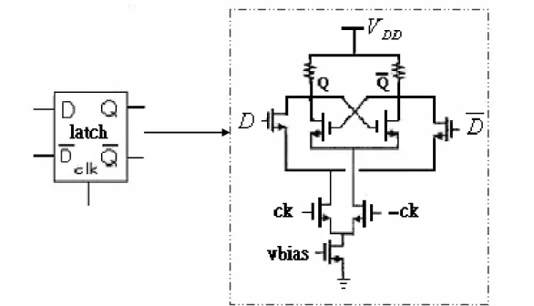
(28) Chapter 3 FREQUENCY SYNTHESIZER In multi-frequency wireless transceivers, frequency synthesizer is an essential part to perform channel switching. Among many different frequency synthesis techniques, the dominant method used in wireless communication industry is the digital PLL circuit, and “Integer-N” frequency synthesizer is widely adopted. Referring to the noise consideration we discussed in the last chapter, the integer-N type has an unavoidable disadvantage that the frequency multiplication (by M) raises the phase noise level by 20 log(M ) dB. In order to improve the phase noise, “Fractional-N” type frequency synthesizer was introduced. According to its name, this type makes the output frequency. fVCO be fractional times to the reference frequency f ref and therefore decline the phase noise. The main advantage of the integer-N type is its functionality, low power, space saving, economy and short settling time. As low current and low power consumption is the important issue in commercial applications, I choose the integer-N type frequency synthesizer in this thesis. Fig. 11 is the architecture of the Integer-N type frequency synthesizer to be designed.. 17.
(29) Fig. 11 “Integer-N” PLL architecture. In this architecture, the programmable frequency divider is from 1024 to 2047 and the reference frequency is 1MHz. The design consideration and simulation results of each block are shown in the following sections.. 3.1 VCO Design 3.1.1 Complementary & All-NMOS Couple pair VCO In VCO design, there are three kinds of architecture: voltage controlled crystal oscillator, LC-tank oscillator and ring oscillator. Because of its low phase noise and easy integration, LC-tank oscillator is suitable for RF circuit design.. Fig. 12 shows two typical LC-tank oscillators. The first one uses NMOS and PMOS cross-coupled pairs (Complementary cross-coupled pair) to provide negative- Gm and the other employs all-NMOS cross coupled pair. The 18.
(30) complementary topology uses just one inductor in parallel with varactors to build the LC-resonator instead of two inductors in parallel to signal ground. In both structures, MOS cross-coupled pair is an active part to compensate for the losses of inductor and capacitor.. Complementary Coupled pair VCO. Fig. 12. All-NMOS Coupled pair VCO. Two typical LC-tank oscillator structures. There are several reasons that the complementary structure is superior to the all-NMOS structure: [6]. 1.. The complementary structure offers better rise and fall time symmetry. It makes low upconversion of 1/f noise and other low frequency noise sources.. 2.. The complementary structure offers higher transconductance for a given current, which results in a better start-up behavior. 19.
(31) 3.. The DC voltage drop across the channel in the all-NMOS structure is larger since the DC voltage of drain is Vdd .This results in stronger velocity saturation.. 4.. The complementary structure also exhibits better phase noise performance for all bias points illustrated in Fig. 13.. As long as the oscillator operates in the current limited regime, the tank voltage swing is the same for both oscillators. However if we desire to operate in the voltage limited region, the all-NMOS structure can offer a larger voltage swing.. All-NMOS. Complementary. Fig. 13 Phase noise simulation results for both structures. 3.1.2 Design for Low Power and Low Phase Noise In wireless communications, low power and low noise are very critical, so 20.
(32) does in VCO design. Fig. 14 is the description of LC resonator tank where R represents the loss of capacitor and inductor.. Fig. 14. Basic LC resonator tank. Using the energy conservation theorem, the maximal energy stored in the inductor is equal to the maximal energy stored in the capacitor: 2 CV peak. 2. =. 2 LI peak. 2. The peak loss in the tank is written as. 2 Ploss = RI peak =C. where wc =. R 2 V peak L. or. 2 Ploss = RC 2 wc2V peak =. R 2 V peak L wc2 2. 1 is the center frequency. LC. From these equations, for the unavoidable series resistance in the resonance tank, one can increase the inductance in order to decrease the power loss.. In 1996, Leeson [7] derived the following expression for the single-side band phase noise power spectral density of an LC-tank VCO as:. 21.
(33) S SSB. kT wc2 =F 2 Psig Q 2 ∆w2. (10). where Q is the loaded quality factor for the tank, ∆w = 2π∆f is the angular frequency offset, F is called the device excess noise factor or simply noise factor, k is the Boltzmann’s constant and T is the absolute temperature. Eq. 2 , (10) shows the obvious way to reduce phase noise is to increase Psig ∝ V peak. and the most efficient way is increasing the Q factor of the tank. According to the Barkhausen oscillation criterion, the phase stability definition for Q is more appropriate for oscillator application. The phase stability quality factor is defined as. QPS = −. 1 L L wc dφ = = wc 2 dw w = wc R C C. It reveals that the increase of the L / C ratio will increase QPS , thereby improving phase noise. But there is a tradeoff between L / C ratio and tuning range, so one should decide the maximum L / C ratio according to its minimum tuning range which the system can tolerate.. From above, we make Table. 4 and design our R, C value to optimize low power and low phase noise in the specified center frequency.. Low Power. 22. Low Phase Noise.
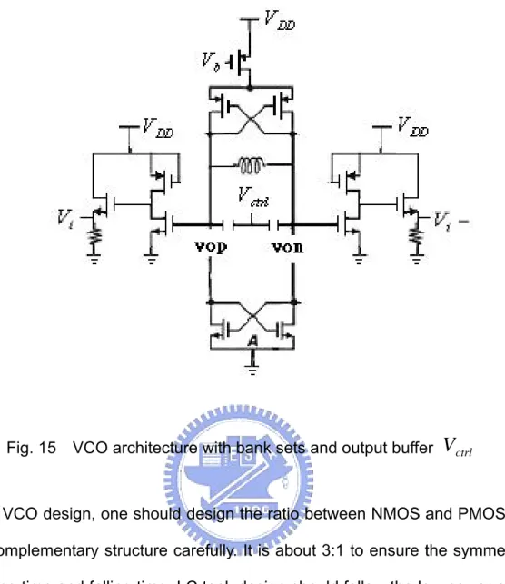
(34) Inductor (L). Maximize. Maximize. Capacitor (C). Minimize. Minimize. Resister (R). Minimize. Minimize. 1/ 2 Amplitude ( V peak ∝ Psig ). minimize. maximize. Table. 4 Low-Power & Low-Phase noise Optimization Summary. 3.1.3 Architecture and Simulation As described before, there are several advantages inherent in the complementary topology. So we take it to realize our VCO. Fig.15 is the complete circuit with VCO, bank sets and output buffers.. 23.
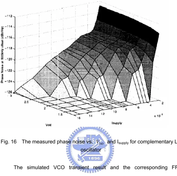
(35) Fig. 15. VCO architecture with bank sets and output buffer. Vctrl. In VCO design, one should design the ratio between NMOS and PMOS in the complementary structure carefully. It is about 3:1 to ensure the symmetry of rising time and falling time. LC tank design should follow the low power and low phase noise design issue. Accordingly, larger inductor should be chosen to enhance the Q factor of the tank, and we can get capacitor value with. wc =. 1 . A PMOS current source bias at Vb in the top can regulate the LC. current flow into VCO and decrease VDD sensitivity. VDD is 1.5V to reduce power consumption and obtain better phase noise. Referring to Fig. 16, it is shown that a lower supply voltage has better noise performance. To avoid the manufacture variation and lack of tuning range due to small adopt three sets of varactor bank to compensate for it.. 24. L ratio, we C.
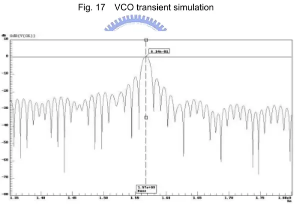
(36) Fig. 16 The measured phase noise vs. VDD and Isupply for complementary LC oscillator The simulated VCO transient result and the corresponding FFT simulation are shown in Fig. 17. Fig. 18 is its FFT simulation. We see that the output swing of VCO is 1.33 Vp-p and the swing is reduced to 0.28 Vp-p after buffer. The DC value of the output buffer is about 0.4V, being too low to push the frequency divider. Thus we raise the buffer output to 0.85V and then send the signal to the next stage.. 25.
(37) Fig. 17. VCO transient simulation. Fig. 18. VCO FFT simulation. Fig. 19 shows the tuning range of VCO. In our design, it has 50MHz tuning range from 1.55 to 1.60GHz (3.1%). A narrow tuning range will decline the frequency sensitivity to the control voltage ( Vctrl ) and decrease the settling time. 26.
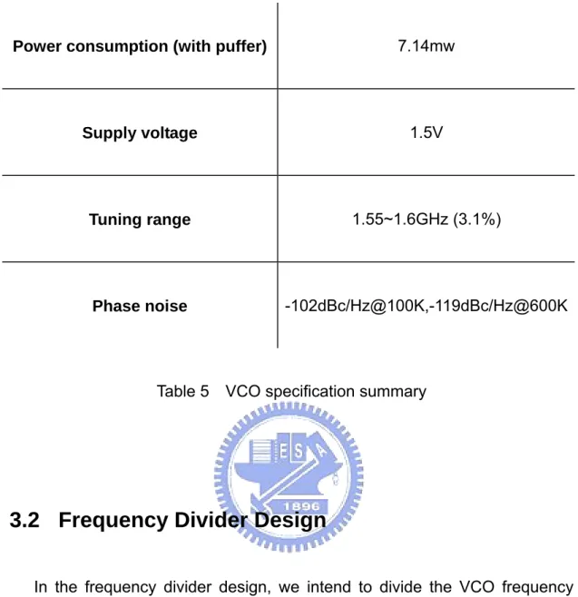
(38) In this design, KVCO is about 33.3MHz/V.. Fig. 19. VCO tuning range simulation. Phase noise simulation result is shown as in Fig. 20. At 100 KHz and 600 KHz offset from the carrier, phase noise is -102dBc/Hz and -119dBc/Hz, respectively. Table. 5 is the simulation results of VCO:. Fig. 20 VCO phase noise simulation. 27.
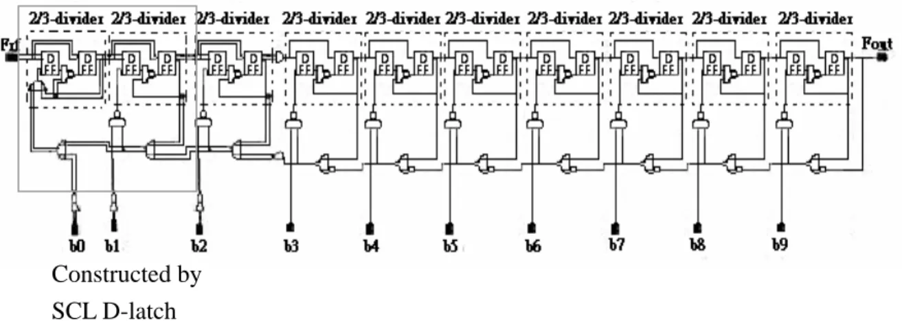
(39) Power consumption (with puffer). 7.14mw. Supply voltage. 1.5V. Tuning range. 1.55~1.6GHz (3.1%). Phase noise. -102dBc/Hz@100K,-119dBc/Hz@600K. Table 5. VCO specification summary. 3.2 Frequency Divider Design In the frequency divider design, we intend to divide the VCO frequency down to 1MHz of reference frequency. Our VCO frequency is about 1.57GHz, and we construct the programmable divider by ten divide-by-2/3 stages which were shown in Fig. 21. The dividing ratio is from 1024 to 2047. bo to b9 are control bits that switch each stage to divide-by-2 or divide-by-3 mode by changing. the input level of each bit. Programmable divisor is given as 10. N = 1024 + ∑ bn ⋅ 2n . n=0. 28.
(40) Constructed by SCL D-latch Fig. 21. Frequency divider architecture. As illustrated in the figure, each divide-by-2/3 stage consists of two D-flipflops, an AND gate and an OR gate. Fig. 22 shows the block diagram of each D-flipflop made of two D-latches and one inverter.. Fig. 22. Block diagram of a master-slave D-flipflop. The maximum operation frequency of divider is determined by the speed of D-latches. At low frequencies, CMOS logic is desirable. However, at high frequencies Source Coupled Logic (SCL) is more suitable because of its high speed and low power consumption. Fig. 23 shows the SCL D-latch structure.. 29.
(41) Fig. 23. SCL D-latch structure. The first two stages of the frequency divider must operate at high frequencies (GHz or hundreds MHz) and CMOS logic circuit can’t handle them. We carry out SCL D-latch structure as shown in Fig. 24. These stages are realized in a differential SCL and logic gates are embedded in it, whose speed will be restricted by the parasitic capacitor. If the parasitic capacitor is too large, voltage of n1 and n2 can’t be charged promptly and the divider function will be seriously affected. To avoid this problem, layout must be very careful.. 30.
(42) Fig. 24 Differential Source Coupled Logic. Fig. 25 is the VCO& frequency divider simulation results. We set VCO DC voltage at 0.85V to ensure gate voltage of each input MOS (input ck in Fig. 24) be high enough and operate accurately. VCO frequency (CK) is divided by 1568 and the output frequency (FDIV) is about 1MHz, being very close to the reference frequency.. 1us. 31.
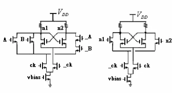
(43) Fig. 25. VCO& Frequency divider simulation result. With variation during fabrication, the frequency of VCO may drift to the higher frequency range, so in our simulation we should guarantee this divider still work at 1800MHz. In the power consumption issue, because we use SCL logic and low supply voltage, it only consumes 7.32mW.. 3.3 Phase/Frequency Detector Design In phase frequency detector design, three-state detector is widely used because: it’s linear range is ± 2π radians, being wider than ± π of two-state, and it can be used as frequency and phase detector. So it is taken in our design and is illustrated in Fig. 26.. Fig. 26. Phase/Frequency detector architecture 32.
(44) In this work, we use the falling edge trigger module. f ref is an 1MHz off-chip oscillator output frequency. When the falling edge of f ref arrives before the falling edge of f div , VCO frequency must be raised up to catch f ref , and the output upp will be set (Refer to Fig. 27). On the other hand, if the falling edge of f div arrives prior to the falling edge of f ref , it represents that VCO is faster than the reference signal and should be slow down. In this case. dwp will be set (Refer to Fig. 28). However, this PFD has a serious limitation for its “dead zone”. Dead zone causes jitter in PLL and should be removed. For this purpose, we add two inverters to form a delay chain in the reset path, thereby generating enough delay to eliminate the dead zone of PFD [8].. Fig. 27. f ref. is faster than f div and upp is set. 33.
(45) Fig. 28. f div is faster than f ref and dwp is set. 3.4 Charge Pump Design 3.4.1 Single-Ended & Differential Charge Pump Single-ended charge pumps are popular since they don’t need loop filters and offer low power consumption with tri-state operation. Fig. 29 shows a single-ended charge pump with switch at drain.. A fully differential charge pump (Fig. 30) has several advantages over the conventional single-ended charge pump.. 1. Switch mismatches between NMOS and PMOS doesn’t substantially affect the overall performance.. 34.
(46) 2. This configuration doubles the range of output voltage compliance compared with the single-ended charge pump. For low voltage operation (1.5V in our design), the limited output voltage range will restrict the tuning range of VCO.. 3.. The differential output stage is less sensitive to the leakage current since the leakage current behaves as a common-mode offset with the dual output stages.. 4.. The differential charge pump with two loop filters provides better immunity to the supply, ground and substrate noise when on-chip filters are used.. Fig. 29. 3.4.2. Single-ended charge pump with switch at drain. Architecture and Simulation. Owing to the above considerations, we choose a differential, three-state charge pump in our design. The three-state gives an output current ± I p or zero, depending on the control signals from the phase detector. And it is 35.
(47) followed by a passive loop filter that translates the output current I cp to the control voltage Vctrl of VCO. The structure consists of three parts: the current source, the current sink and switches as illustrated in Fig. 30.. M1. M2. Down. Up. Down. M3. Up. M4. Fig. 30 Differential charge pump architecture. In Fig. 30, M1 through M4 and the current source can offer a fixed current to the switches. These switches are controlled by upp , upn , dwp and dwn generated from phase detector whereas two them form of a. complementary pair. These complementary signals can assure the current always flow through M2 and M4. When upp and dwn are set, the current flows into the loop filter, and current flows out of the loop filter when dwp and. upn are set (refer to Fig. 30). This can also reduce the switch noise. According to our design, the simulation of current I cp is about 115uA (shown in Fig. 31) and the corresponding power consumption is 0.64 mw.. 36.
(48) Fig. 31 The simulation of Icp when upp and dwp are set. 3.5 Loop Filter Design As discussed in chapter 2, loop filter has close relationship with PLL behaviors. In our design, we choose a second-order passive loop filter and practice it off-chip to minimize chip size. The architecture is shown as below.. Fig. 32. Passive loop filter architecture 37.
(49) 3.6 Complete Loop Simulation & Layout The architecture and simulation of each block are introduced in the previous sections. Now we combine all of them and carry out simulation. Figs. 33 & 34 show the settling time when fixing one channel and then sweep to another. The settling time is 80us for fixed channel, and Vctrl needs 180us to achieve the stable condition when switch to another channel (divide number from 1568 to 1572). The layout of the synthesizer is shown as in Fig. 35.. Fig. 33 Settling time simulation with fix channel. 38.
(50) Fig. 34. Settling time simulation when sweeping channel. Fig. 35. Layout of the synthesizer 39.
(51) Chapter 4 MEASUREMENT RESULTS During the measurement, we found a serious problem in the VCO so that the PLL can’t work successfully with this problem. In this chapter, we will find out the problem and use other methods to measure the frequency divider, the phase/frequency detector and the charge pump. Fig. 36 shows the die photo.. Fig. 36 Die photo There are many pads of synthesizer chip, we usually measure it on PCB rather than on wafer, thus the order of pads doesn’t need to follow the G-S-G. 40.
(52) (DC pad) or S-G-S (RF pad) rule. But during the frequency divider measurement, the clock signal must input from outside to substitute the VCO, and we don’t consider the order of pad at first. This makes us to input one RF signal ( vi − ) with DC probe at first measurement. A DC probe doesn’t have good performance at high frequencies, for instance the reflection coefficient S11 is not low enough and there is a power mismatch problem between two. input clocks of frequency divider. Thus, the layout is very critical, and we should fulfill the rule as possible as we can.. 4.1 VCO measurement During measuring the VCO, there is no oscillation at output and we measure the DC value of each part to figure out the problem. Fig. 37 marks all points that their voltages and currents can be measured.. Control voltage and Switch voltages of three banks. Fig. 37 All measurable points of VCO 41.
(53) 1. When vctrl , vc1 , vc 2 and vc 3 at floating, the current of VCO is about 4.55mA; it is close to the simulation result (4.76mA), being enough to supply the VCO to oscillate.. 2. The DC voltage of the buffer output ( Vi ) is 0.6V. Although it is a little higher than the simulation value (0.4V), but is still in the normal region.. 3. We connect vctrl to a power supply, to tune the varactors. When Vdd was turned on, we find that vctrl will increase with Vdd if Vdd is higher than 0.7V. vc1 , vc 2 and vc 3 are also in the same situation. Thus we know the problem occurring at varactor.. 4.1.1 What is the problem with varactor? We have already understood that the problem comes from the varactor. The voltage of vctrl shouldn’t change with Vdd if the varactor is normal. We try to use some methods to verify that the varactor is just like a resistor with very low resistance.. 1. We add a 1.3KΩ resister between vctrl and ground, the voltage of vctrl should be normally zero because the varactor is open at DC. But we observe the voltage changes from 0.707V to 0.681V. It indicates that the varactor behaves like a resister doing voltage divide.. 2. When we bias vc1 , vc 2 and vc 3 at 1.5V in order, vctrl will raise from 0.58V to 1.23V. It indicates that the varactor of each bank doesn’t work, so that 42.
(54) vctrl changes with them.. 3. The current of VCO is about 4.55mA when vc1 , vc 2 , vc 3 and vctrl are all floating. After they are connected to a power supply with 0V, the output current lifts to 10.1mA or more. This demonstrates that there is a DC current path flowing through the varactor to the ground so as to increase the current.. 4.. There are only probe pads at vop and von , but we use special instrument to measure their DC voltages and find vop rises from 0.707V to 0.93V when vctrl is connected to a power supply.. 5. The resistance between vc1 , vc 2 , vc 3 and vctrl should be very large (several M Ω ). But we use an electrical meter to measure it and find out the resistance is 23Ω , 21.3Ω and 20.3Ω between vctrl and vc1 , vc 2 , vc 3 . It is very low and just likes a small resistor. All chips have the same problem so that the PLL can’t work successfully since the VCO can not oscillate. As we can’t measure the loop performance, we try to use other methods to verify other parts of the chip, and this problem will be discussed later.. 4.2 Frequency divider measurement As described before, there is no oscillation at VCO output, and thus no 43.
(55) input signal at the frequency divider. We try to input signal to the frequency divider from outside and probe each pad of the divider to see if it works successfully or not. We bond wire von and vop ,and input them from SMA to avoid the mismatch problem. Fig. 38 is the photograph of PCB.. Fig. 38. PCB of frequency divider measurement. The total current consumption of the frequency divider is 4.4mA (6.6mW), being a little smaller than the simulation value (7.32mW).. During measurement, we use a spectrum analyzer (Aglient E4407B), a signal generator (Aglient E8247C) and a probe station, Fig. 39 shows their photographs.. 44.
(56) Fig. 39. Photograph of instruments. We set the input signal frequency at 1.57GHz, its power level is 0dBm and the DC voltage is 0.85V. Then we probe the 11x11um probe pad of each stage as illustrated in Fig. 40.. 45.
(57) Fig. 40 Probe pad photo. The probe pad is very important for circuit debug whose structure was shown in Fig. 41. If there is no probe pad in the circuit, we never know any part will work or not. Like vop and von , these two probe pads let us know the DC variation after connecting vctrl with power supply, and probe pads at the frequency divider let us know the output frequency of each stage. There are also probe pads at PFD. The size of these probe pads are 11x11 um 2 , but the minimum size of the hard probe used in CIC is 12x12 um 2 , which is a little bigger than the probe pad, and is difficult to be used. Therefore, we should increase the size of the probe pad to 12x12 um 2 .. 46.
(58) Fig. 41 Probe pad diagram. Figs. 42 and 43 show the spectrum of the first stage output of frequency divider. We set it at divide-by-2 and divide-by-3 model, respectively, and get a frequency at 785MHz and 525MHz. Because the input RF signal is very strong, the probe also receives it and has a peak at 1.57GHz shown at spectrum analyzer.. 47.
(59) Fig. 42 First stage sets to divide-by-2 model. Fig 43 First stage sets to divide-by-3 model 48.
(60) The spectrum of the second stage output of frequency divider was shown in Figs. 44 and 45. Fig. 44 is the spectrum when only first stage is set to divide-by-3 model and Fig.45 is the spectrum when both of them are set to divide-by-3 model.. Fig. 44. Only the first stage is set to divide-by-3 model. 49.
(61) Fig. 45. Both of the first and the second stage are set to divide-by-3 model. The divisor N of the programmable divider is from 1024 to 2047 controlled by b0 to b9 , b9 is always set to high and b7 , b6 , b4 , b3 are always set to low. Figs. 46 and 47 are the spectrum when N=1536 and 1575.. 50.
(62) Fig. 46. Fig. 47. Output spectrum when divide-by-1536. Output spectrum when divide-by-1575 51.
(63) 4.3 PFD and charge pump measurement When measuring PFD and charge pump, we input the clock signals from SMA at first, after frequency dividing, the signal f div is sent to the PFD and compares with the reference clock f ref to generate the up/down signal, then sent to charge pump. Fig. 48 is the spectrum of the reference oscillator, from the spectrum analyzer, we know that the oscillator generates square wave, and has so many side lobes.. Fig. 48. The spectrum of the reference oscillator. We try to measure the waveform of the charge pump current, but the oscilloscope can only display the voltage waveform. Thus we connect the loop filter and use a multimeter to measure its DC voltage. If N=1536,. f div =1.022MHz, it is always higher than f ref , then the I cp will pull down the VCO frequency during the very short time, and we measure the voltage is 0V 52.
(64) (Fig. 49).. Fig. 49. f div is higher than f ref , Vctrl is pulled down to 0V. On the contrary, if we set N=1575, f div =0.996MHz, VCO frequency will be pulled up, and voltage is raised to 1.5V (Fig. 50). In this figure, we know that PFD compares f div with f ref to generate an up/down signal every 1u sec, so that there is a little pulse at charge pump output waveform. In spectrum, this is what we called “spur noise”. The peak-to-peak voltage is 122mV, and I cp is 122uA under the DC 1MΩ load condition.. 53.
(65) 1us. Fig. 50. f div is lower than f ref , Vctrl is pulled up to 1.5V. Then we change the input frequency to 1536MHz and 1575MHz, f div is equal to f ref , the voltage is 0.654V when N=1536 and 0.886 when N=1575. The current consumption of the charge pump is 0.5mA (0.75mW), and the power consumption of PFD is less than 1mW. Table. 6 is the summary of the power consumption.. 54.
(66) Simulation. measurement. VCO. 7.14mW. 6.8mW. Frequency divider. 7.32mW. 6.6mW. Charge pump. 0.64mW. 0.75mW. I cp. 115uA. 122uA. PFD. <<1mW. <<1mW. Whole chip. 15.1mW. 14.1mW. Table. 6. Power consumption summary. 4.4 Discussion The simulation and measurement results of power consumption are very close, and all parts work successfully except the VCO. The previous measurements use a signal generator to generate the clock signal for the frequency divider. Signal power and frequency can be fully controlled, but since it is not a close loop, the loop settling time can’t be measured without a control voltage feedback to the VCO. The frequency divider still works even we input the clock signals from SMA. It seems that we can use another VCO to substitute the on-chip one, which has the same frequency and tuning range. But it is hard to find a single VCO chip because most of the design houses sell a whole module instead of a single VCO chip. The GPS system operates at 1.57GHz, it is not a common specification, in contrast 900MHz, 1800MHz or 2.4GHz VCO is easier to find. If we find such a VCO is available, the whole 55.
(67) loop can be set up as illustrated in Fig. 51. The practical PCB layout would be constructed after concerning about the arrangement of the external VCO pads.. Fig. 51. Loop diagram with external VCO. 56.
(68) Chapter 5 CONCLUSIONS AND FUTURE PROSPECTS The measurement results are described previously, and due to the problem with varactor, we can’t measure the VCO phase noise and loop settling time. In this chapter, we discuss the possible reasons and learn some useful experiences in this tape out, and then build the future prospects.. 5.1 Conclusions The varactor model is supplied from TSMC, and was used in previous tape out, thus the model is correct. Additionally, DRC and LVS of the layout were also verified. Thus, the problem may come from fabrication. All parts of the synthesizer work successfully except the VCO. The frequency divider divides the input frequency accurately, PFD can compare with f div and f ref to generate the corresponding up/down signals, charge pump generates the current I cp and transfers into Vctrl after loop filter.. The. measurement of power consumption is 14.1mW with 1.5V supply voltage, it is very low power and achieve our design purpose.. 5.2 Future Prospects 57.
(69) In the design of VCO, a start-up circuit can be integrated into the VCO architecture in future tape out to ensure that the circuit can start to oscillate. The start-up circuit will turn off automatically to save power after VCO starting to oscillate. In simulation, we should add the bond wire effect into it, the parasitic inductance is about 1nH per 1mm, and we should enlarge the simulation range of the resister variation to 10%. Furthermore, the RF output pad must be close to the circuit, the metal line should be as wide as possible and less corner is desirable to reduce parasitic inductance. These design considerations are helpful to design a successful frequency synthesizer in high frequency region.. 58.
(70) REFERENCE [1] Derek K. Shaeffer, Stanford University, Thomas H. Lee, Stanford University, “The Design and implementation of low-power CMOS radio receivers” KLUWER ACADEMIC PUBLISHERS. [2] Farbod Behbahani, Member, IEEE, Hamid Firouzkouhi, Member, IEEE, Ramesh. Chokkalingam,. Siamak. Delshadpour,. Alireza. Kheirkhahi,. Mohammad Nariman, Student Member, IEEE, Matteo Conta, and Saket Bhatia “A fully integrated low-IF CMOS GPS radio with on-chip analog image rejection”, IEEE JOURNAL OF SOLID-STATE CIRCUITS, VOL. 37, NO. 12, DECEMBER 2002. [3] Giampiero Montagna, Giuseppe Gramegna, Ivan Bietti, Massimo Franciotta, Member, IEEE, Andrea Baschirotto, Senior Member, IEEE, Placido De Vita, Roberto Pelleriti, Mario Paparo, Member, IEEE, and Rinaldo Castello, Fellow, IEEE “A 35-mW 3.6mm 2 Fully Integrated 0.18-um CMOS GPS Radio”, IEEE JOURNAL OF SOLID-STATE CIRCUITS, VOL. 38, NO. 7, JULY 2003. [4] Valence Semiconductor , Inc. VS7001 “A GPS front end downconverter” JAN 2002. [5] Hamid R. Rategh, Tavanza, Inc., Thomas H. Lee, Stanford University, “ Multi-GHz frequency synthesis & division, Frequency synthesizer design. 59.
(71) for 5GHz wireless LAN systems”. [6] Ali Hajimiri, Thomas H. Lee, Center for Integrated Systems, Stanford, CA 94305-4070, USA “Phase noise in CMOS differential LC oscillators”, IEEE 1998. [7] D. B. Leeson, “A simple model of feedback oscillator noise spectrum”, Proc. IEEE, pp. 329-330, Feb. 1966.. [8] F. M. Gardner, “Phase lock Techniques”, New York, NY: John Wiley & Sons, 1979.. 60.
(72) PUBLICATION REMARKS 1.. VLSI-2004 (Las-Vegas, USA). 2.. PIERS 2004 (Nanjing, China). 61.
(73)
數據
+7
相關文件
Promote project learning, mathematical modeling, and problem-based learning to strengthen the ability to integrate and apply knowledge and skills, and make. calculated
Wang, Solving pseudomonotone variational inequalities and pseudocon- vex optimization problems using the projection neural network, IEEE Transactions on Neural Networks 17
Comparison of B2 auto with B2 150 x B1 100 constrains signal frequency dependence, independent of foreground projections If dust, expect little cross-correlation. If
In section29-8,we saw that if we put a closed conducting loop in a B and then send current through the loop, forces due to the magnetic field create a torque to turn the loopÆ
questions and we are dedicated to are dedicated to are dedicated to are dedicated to future research and development to bring you the future research and development to bring you the
* School Survey 2017.. 1) Separate examination papers for the compulsory part of the two strands, with common questions set in Papers 1A & 1B for the common topics in
Microphone and 600 ohm line conduits shall be mechanically and electrically connected to receptacle boxes and electrically grounded to the audio system ground point.. Lines in
SDP and ESDP are stronger relaxations, but inherit the soln instability relative to measurement noise. Lack soln
