國 立 交 通 大 學
光電工程研究所
碩士論文
利用非等向性蝕刻氮化鎵與藍寶石基板介面
製作高效率紫外光發光二極體
High Efficient UV LED with Anisotropically Etched
GaN-sapphire Interface
研究生:洪政暐
指導教授:郭浩中 盧廷昌 教授
中 華 民 國 九 十 八 年 七 月
I
誌 謝
兩年的研究生生活即將結束,在交大所學到的知識及經驗相當的充
實,首先,我要感謝的是郭浩中老師及盧廷昌老師,使我在實驗上有機
會開創新的領域,更感謝明華、清華學長們的提攜與幫忙,讓我們一同
完成新的創新構想。回想起過去的這兩年,我從 LED Team 轉到了
VECSEL Team 接著又轉到了 Epi Team,因此,我也吸收到了許多不同
的知識,最有趣的堪稱是 HVPE 的裝機時期,與 Dr. Alan gott 學習到了
許多磊晶與裝機的知識與經驗,另外,也要感謝工研院的主立學長提供
我們量測的樣品,讓我可以在 OPT 光電年會安然度過。
再來當然就是要感謝我們 Epi Team 的成員,朝勳學弟跟依嚀學妹,
另外我也要感謝和我一同來交大奮鬥的同袍戰友小柯、超帥的治凱、老
實的建綱、玫君、睿中、亭均、立夫、勁生、尚樺,在這段期間中,多
虧有你們的幫忙與協助,不論再量測或製程,才讓我在畢業的前就能夠
有優良的研究成果,並且獲得 Appl. Phys. Lett.期刊的肯定。
在交大的這段時間裡,歡樂的氣氛與笑聲總在實驗室裡迴繞著,雖
然時間只有短短的兩年,但在我的回憶裡可是寫滿了好幾頁,謝謝你
們,我會記得這裡的點滴,用揚起的嘴角回想相聚在一起的歡樂時光,
祝各位事事順心。
II
Abstract
We report the fabrication and study of high efficient UV light emitting diodes (UVLED) with inverted pyramid microstructures at GaN-sapphire interface. The HIP
structures were created by anisotropic chemical wet etching. The UV LED was fabricated by growth interrupt, chemical etching, and regrowth processes. The as grown sample
showed reduction of dislocation density in the cross-section TEM images and narrow XRD rocking curves. The ML-ELOG mechanism might elucidate the reason for
threading dislocation reduction. The electroluminescent output power at normal direction was enhanced by 120% at 20 mA operating current and the output power integrated over
all directions was improved by 85% compared to a reference sample.
The ray tracing simulation and three-dimension far field pattern experimental results
of UVLED with HIP GaN/air structure are reported. The HIP structure could reduce the view angle, which redirects the escape light employed by optical geometric property and
refraction index difference within GaN/air/Sapphire. The UVLED with inverted pyramid structures have significantly enhanced the light extraction efficiency and at the same time
also improved the crystal quality by partially relieving the strain and reducing the dislocation defects in ML-ELOG regrowth process.
III
sapphire substrate with thermal bonding process for fabricate thin GaN LED. Indeed we
have had successfully remove sapphire substrate by mechanical lift-off to develop the large area lift-off by HIP structure.
IV
摘要
我們提出於氮化鎵和藍寶石基板介面製作倒六角型金字塔結構,以
提高紫外光發光二極體的效率。該倒六角形金字塔結構係由非等向性化
學蝕刻而成。該紫外光發光二極體,歷經磊晶中斷、蝕刻後再成長的過
程。我們分別從 TEM 剖面圖及 XRD 中,觀察及量測到較少的穿透缺陷
與較窄的晶體繞射半高寬。我們提出了多階層側向磊晶(ML-ELOG)機制
以解釋穿透缺陷減少的原因。該樣品在 20 毫安培的注入電流下,其電
激發光之軸向光發光強度相較於參考片提升了 120%,而積分強度則提
升了 85%。
我們透過光追跡模擬及遠場光學實驗,以佐證紫外光發光二極體具
倒六角型金字塔結構下之量測結果。此具倒六角型金字塔結構之發光二
極體,可藉由氮化鎵-空氣-藍寶石基板間的折射率差異與幾何結構,使
光線得以重新導正至軸向光因而使視角減小。此倒金自塔結構可有效提
高發光效率,並可藉由部份的應力釋放及多階層側向磊晶機制以減少氮
化鎵中穿透缺陷來提高磊晶的晶體品質。
此外,我們可利用該此倒金自塔結構於介面造成的脆弱特性,近一步
使用熱壓法去除藍寶石基板以製作 thin-GaN 發光二極體。實際上,我們
亦已大面積地利用該結構以機械式剝離法剝離藍寶石基板。
V
Catalog of contents
Chapter 1 Preface
1.1 Introduction ··· 1
1.2 Development status of GaN-based UV LED ··· 2
1.3 Motivation and other techniques comparison ··· 4
1.4 Reference ··· 13
Chapter 2 Properties and Types of defect in crystalline lattice
2.1 Brief introduction about defects ··· 152.2 Burgers vector ··· 17
2.3 Point defects ··· 18
2.4 Stacking faults ··· 18
2.5 Screw, Edge and Mixed dislocations ··· 19
2.6 Jogs and Kinks ··· 21
2.7 Climb ··· 22
2.8 Dislocations in crystal growth ··· 22
VI
3.1 Etching process in molten KOH ··· 26
3.2 Scanning electron microscope-Cathodoluminescence (SEM-CL) ··· 30
3.3 Atomic force microscope (AFM) ··· 31
3.4 Transmission electron microscope (TEM) ··· 34
3.5 X-ray diffraction (XRD) ··· 36
3.6 Photoluminescence spectroscopy (PL) ··· 40
3.7 Electroluminescence spectroscopy (EL) ··· 41
3.8 Reference ··· 42
Chapter 4 Analysis of UVLED regrown on HIP GaN substrate
4.1 Fabrication of UV LED epitaxial structure ··· 444.1.1 Process flow of HIP-structure LED ··· 44
4.2 Material properties analysis 4.2.1 Surface morphology analysis of HIP structure ··· 47
4.2.2 Roughness analysis by AFM after LED regrowth ··· 48
4.2.3 X-ray diffraction analysis ··· 49
4.2.4 Defects formation analysis by TEM··· 51
VII
4.3 Optical properties analysis of UV-LED regrown on HIP GaN substrate
4.3.1 Photoluminescence spectrum ··· 54
4.3.2 Far-field optical pattern ··· 56
4.3.3 TracePro geometrical optics simulation ··· 57
4.4 Electrical properties analysis of UVLED regrown on HIP GaN substrate 4.4.1 Electroluminescence spectrum ··· 59
4.4.2 Current-dependent EL intensity ··· 60
4.4.3 L-I-V characteristic curve analysis ··· 61
4.4.4 Observation of Leakage current ··· 62
4.5 Reference ··· 63
Chapter 5 Mechanical lift-off by HIP-structure
5.1 Mechanical lift-off process flowchart ··· 655.2 Material properties analysis 5.2.1 GaN-sapphire interface morphology analysis after mechanical lift-off · by SEM ··· 67
5.2.2 GaN-sapphire interface morphology analysis after mechanical lift-off by AFM ··· 68
1
Chapter 1 Preface
1.1 Introduction
Since 1960 to nowadays, light-emitting diodes (LEDs) have been extensively utilized to amount of optoelectronic display product. Because the rapidly increase of lightness and the green, blue and ultraviolet LEDs have been well developed, the extended field of applications will bring unlimited business opportunities. The main growth was comes from the global automotive exterior LEDs, small-middle type liquid crystal display (LCD) backlight module and solid-state lighting market. The III-nitride based direct and wide bandgap compound semiconductors could emit wavelength range from ultraviolet to infrared, which has covered all of visible light. However, owing to lack of group III-nitride single crystal bulk, the heteroepitaxial on foreign substrate general result in extremely bad crystalline.
Until 1971, Pankove laboratory successful manufactured the first nitride-based LED. But the most of III-nitride based semiconductors were still deposited on foreign substrate, such as 6H-SiC, Si and sapphire (Al2O3) to date [1]. The obstacles
result from large lattice mismatch, thermal expansion coefficient mismatch and could not obtain the well epi-quality at p-type GaN, which led to the LED development without eminent breakthrough. In 1986, Amano research group employed the
2
metal-organic chemical vapor phase deposition (MOCVD) system to grow a thin AlN buffer layer at low-temperature (LT) for decrease the dislocation density, which method could obtain the mirror-like thin films [2]. In 1991, Nakamura used the LT GaN buffer layer could acquire the high crystal quality and mirror-like thin films as well [3]. In 1989, Amano research team was the first one used the low-energy electron-beam irradiation (LEEBI) to irradiate the surface of Mg doped gallium nitride then got p-GaN, which dopant concentration could reach to 1017 cm-3 and about 12 Ω-cm sheet resistance [4]. Nakamura technical group found that once the Mg doped gallium nitride under the high temperature and sufficient N2 surroundings,
then low sheet resistance p-GaN could be obtained [5]. The nitride-based compound semiconductor rapidly developed in past decade. The Japanese Nichia company had reported the luminous efficiency could achieve to 150 lm/W in 2006, 169 lm/W in 2007 and even promote to 249 lm/W in 2009.
1.2 Development status of GaN-based UV LED
White-light LEDs have been widely used to replace the conventional illumination, which with advantages like small volume, long lifetime, saving more energy and low power consumption. Thus, it was regarded as the main illumination light source in 21
3 century.
There are three ways of producing high intensity white-light using LEDs. The first way was to use individual LEDs which emit three primary colors-red, green, and blue (RGB), then mix all the colors to produce white light [6]. Hence this method is called multi-colored white LEDs (or referred as RGB LEDs). Because the mechanism was involved with sophisticated electro-optical design to control the blending and diffusion of different colors and relative expansive cost, this method was rarely been used to mass produce white LEDs in industry. The second way was to utilize yellow phosphor material to convert monochromatic light from blue to white-light, the resultant LEDs were called phosphor based white LEDs. The third method is to use ultraviolet LEDs to pump three primary phosphors convert to broad spectrum white-light. The design and production of the light source or light fixture using a monochrome emitter with phosphors conversion was much simpler and cheaper than complex RGB system. Therefore, the majority of high intensity white LEDs recently on the market were manufactured employing phosphor light conversion [7].
As mentioned to the UV LEDs, it has been demonstrated that the low-indium-composition UV LEDs were more sensitive to the threading dislocation
4
density (TDD) than the other high-indium-composition visible LEDs [8]. Because of the immiscibility of indium atoms in GaN material, indium atoms would cluster and formed the quantum-dot like region. These regions with lower energy density of states than multiple-quantum wells (MQWs), generally referred as localized-states [9]. It have been demonstrated the localized states well confine the free electron-hole pairs to radiative recombination, but trapped or cause leakage current pass through the threading dislocations. Except for the TDD, once the emission wavelength was shorter or approaches to 365 nm GaN and particularly p-GaN becomes absorbing, which would cause serious extraction efficiency decrease from active region [10]. Therefore, the purpose of photolithography processes or epitaxial method to reduce threading dislocation density becomes a significant research topic.
1.3 Motivation and other techniques comparison
The main purpose of this study was focus on threading dislocation density reduction and luminous efficiency enhancement. There have several techniques could reduce the TDD by regrowth method; however, some regrowth method might too complex procedure to extensively applied by photolithography technique. We supported a new method to treat the gallium nitride grown on foreign substrate,
5
which generally has high TDD. The way was to utilize potassium hydroxide (KOH) to wet etching the 2 µm GaN thin film, because it has many dangling bonds along the threading dislocations. The high selective etching process was similar to some researches of observing the etching pits density (EPDs), which generally used to fixed-quantity analysis of TDD. That is to say, in this way, the molten KOH solution would etch almost all of dislocations randomly and continuous downward to the bottom of GaN/sapphire interface along the threading dislocations.
All other regrowth or epitaxial techniques for TDD reduction were listed and brief introduce in the following content for promotive comparisons.
1. Epitaxial lateral overgrowth
A. Usui et al. employed epitaxial lateral overgrowth (ELO) technique to reduce the TDD [11]. There are four steps to realize the ELO technique, while the mechanism of it could be observed in Fig. 1.1. First of all, to growth a LT-GaN buffer layer on the substrate. The second step was to growth HT-GaN thin film following the LT-GaN. The third step was use evaporation and lithography technique to make a SiO2 strip-type mask pattern on the GaN
template. Finally to overgrowth GaN thin film in the reaction chamber. Because these SiO2 strips could obstruct TDs and prevent TDs pass through the
6
MQWs along the growth direction. However, the coalescence regions were form new dislocations above the SiO2 strips.
Fig. 1.1 Schematic diagram of the substrate structure in ELOG[11]
2. High pressure growth
Fini et al. and Uchida et al. found that the TDD could be reduced by high pressure and high-temperature growth condition after the low-temperature GaN buffer layer [12-13]. In Fig. 1.2, we could find the main mechanism of discrepancy was the GaN nucleation density and the nucleus size of GaN crystalline. In atmospheric-pressure (AP) series, the GaN buffer layer with higher nucleation density and larger size of nucleus GaN crystalline, which just contrary to the mechanism of the low-pressure (LP) series.
7
Fig. 1.2 Schematic representation of the morphological evolution and associated dislocation generation and propagation in AP and LP series: (a) heat-treated NL on sapphire; (b) nucleation of HT islands; (c) coalescence of HT islands with accompanying TD generation; (d) propagation and interaction of TDs after coalescence [12]
3. Multi-buffer layers
Iwaya et al. have used multi-buffer layers to grow GaN thin films [14]. As shown in Fig. 1.3, LT GaN or AlN buffer layer was first grown at 540oC then ramp up the temperature to 1050oC for growth 1µm high temperature GaN. After that, cooling down the temperature to 540oC and repeat the growth cycle several times, they found the TDD of the GaN could reduce to 107
cm-3-108 cm-3 approximately.
Fig. 1.3 Sequence for growth of GaN employed by two-buffer layer sequence [14]
8 4. SixNy interlayer
Tanaka and Bottcher research group have reported inset a SixNy interlayer
into the high temperature buffer layer could reduce the TDD [15]. The main mechanism was the GaN thin film would grow in 3-dimension (3D) type above the SixNy interlayer; hence the TDs would be interrupted or bent to the
directions perpendicular to the growth direction.
Fig. 1.4 A magnified BF TEM image shows termination of TDs (indicated by arrows) at the interface
5. SiN/GaN buffer layer
The method as shown in Fig. 1.5, the TDD was proposed by Sakai et al., whom grown a SiN on the sapphire substrate before grow the LT-GaN buffer layer, then continuous epitaxy 2 µm GaN [16] as. Sakai found when the SiN layer growth time about 125 seconds, the surface on sapphire would form many micro-holes. These micro-holes approximate have 30 nm size, 1010 cm-2 density and 2 nm height. Sakai suggested that the reason for these micro-holes
9
could reduce the TDD might caused by the function similar to the mechanism in ELO structure.
Fig. 1.5 The schematic illustration of the proposed mechanism involved in the GaN [16]
6. Pendo-epitaxy growth
Davisa et al. utilized the pendeo-epitaxy growth technique to reduce the TDD. There were five steps to realize the method as shown in the Fig. 1.6 [17]. The method and ELO technique have the same purpose in different approaches. The first step was to grow a LT-GaN buffer layer. The second step was to grow HT-GaN thin film. The third step was to use evaporation and photolithography techniques to make SiO2 strip-type pattern. The fourth was to etch GaN thin film downward to the sapphire substrate by dry etching. The fifth was to overgrowth GaN thin film in MOCVD chamber. By tuning the growth parameter, such as temperature, pressure, III/V ratio and N2/H2 composition to
10
(a) (b)
Fig. 1.6 (a) Schematic of PE growth from GaN sidewalls and over a silicon nitride mask. (b) Cross-sectional SEM of a GaN PE growth structure with limited vertical growth from the seed sidewalls and no growth on the seed mask [17].
7. Patterned sapphire substrate
Yamada research group found if the GaN grow on patterned sapphire substrate (PSS), the luminous intensity could be improved, which may cause by the TD reduction and light scattering from the GaN/sapphire interface [18]. The process flow could be seen in Fig. 1.7. The first was to use chemical vapor deposition (CVD) grow the SiO2 film, then dry etching by inductively coupled plasma reactive ion etching (ICP-RIE) and finally growth GaN thin film in the MOCVD. So far, most of epitaxial techniques in industry were using PSS neither ELO nor PE technique, because the later two techniques need longer time to fabricate the patterned substrate.
11
Fig. 1.7 Cross-sectional TEM image of the GaN layer grown on patterned-sapphire substrate [18].
8. Facet-controlled growth
Nitta et al. demonstrated the TDD could be reduced employed by facet-controlled (FC) growth technique under three-step growth GaN [19]. At first, the LT-GaN was grown as buffer layer. In order to increase the 3D-island structures and form the [1010] facet, the epitaxial parameters such as temperature need lower than the HT-GaN and higher pressure under nitrogen surrounding. Nitta found that the geometric type of 3D-islands and [1010] facet would significant effect the TDD, whom reported three possible mechanisms as observed in Fig. 1.8. If the growth time was insufficient or the temperature was too low at growth the FC-GaN layer, there would have small and high density of island as shown in Fig. 1.8(a). This formation would cause numerous TDs produced at the grain boundaries. In Fig. 1.8(b), illustrate the
12
formation of too high growth temperature while grow the FC-GaN layer, there would have mesa above the island. These mesas could not help to interrupt the TDs, thus they tuned the epitaxial temperature, pressure, growth time and the surrounding gases while growth the FC-GaN, then they could obtain the growth mechanism like shown in Fig. 1.8 (c). It was the optimized condition, including the moderate island size and form the [1010] facet, which could interrupt TDs and most of TDs were formed along the [1010] direction.
Fig. 1.8 Schematic dislocation reduction models of three different island and facet formation of FC-GaN: (a) small island size, (b) horizontal plane formed on the islands and (c) optimized island size and {1011} facet formation [19].
13
1.4 Reference
[1] J. I. Pankove, E. A. Miller and J. E. Berleyhesier, RCA Rev. 32, 283 (1971). [2] H. Amano, N. Sawaki, I. Akasaki and T. Yoyoda, Appl. Phys. Lett. 48, 353 (1986). [3] S. Nakamura, Jpn. J. Appl. Phys. 30, L1705 (1991).
[4] H. Amano, M. Kito, K. Hiramatsu and I. Akasaki, Jpn. J. Appl. Phys. 28, L2112 (1989).
[5] S. Nakamura, M. Senoh and T. Mukai, Jpn. J. Appl. Phys. 30, L1708 (1991).
[6] A. Zukauskas, M. S. Schur and R. Gaska, Introduction to Solid State Lighting (Wiely-Interscience, New York, 2002).
[7] I. Moreno and U. Contreras, Opt. Exp. Vol. 15, No. 15, 3607 (2007).
[8] A. Khan, K. Balakrishnan and T. Katona, Nature Photonics 2, 77-84 (2008). [9] M. Hao, J. Zhang, X. H. Zhang and S. Chua, Appl. Phys. Lett. 81, 5129 (2002). [10] D. G. Zhao, D. S. Jiang, J. J. Zhu, Z. S. Liu, S. M. Zhang and H. Yanng, Semicond.
Sci. Technol. 23, 095021 (2008).
[11] A. Usui, H. Sunakawa, A. Sakai and A. A. Yamaguchi, Jpn. J. Appl. Phys. 36, L889 (1997).
The first idea was proposed by
14
[12] P. Fini, X. Wu, E.J. Tarsa, Y. Golan, V. Srikant, S. Keller, S. P. Denbaars and J.S. Speck, Jpn. J. Appl. Phys. 37, 4460 (1998).
[13] K. Uchida, J. Gotoh, S. Goto, T. Yang, A. Niwa, J.I. Kasai and T. Mishima, Jpn. J. Appl. Phys. 39, 1635 (2000).
[14] M. Iwaya, T. Takeuchi, S. Yamaguchi, C. Wetzel, H. Amano and I. Akasaki, Jpn. J. Appl. Phys. 37, L316 (1998).
[15] S. Tanaka, M. Takeuchi and Y. Aoyagi, Jpn. J. Appl. Phys. 39, L831 (2000). [16] S. Sakai, T. Wang, Y. Morishima, Y. Naoi, J. Cryst. Growth 221, 334 (2000). [17] R. F. Davisa, T. Gehrkea, K. J. Linthicumb, J. Cryst. Growth 225, 134 (2001).
[18] M. Yamada, T. Mitani, Y, Narukawa, S. Shioji, I. Niki, S. Sonobe, K. Deguchi, M. Sano and T. Mukai, Jpn. J. Appl. Phys. 41, L1431 (2002).
[19] S. Nitta, J. Yamamoto, Y. Koyama, Y. Ban, K. Wakao and K. Takahashi, J. Cryst. Growth 272, 438 (2004).
15
Chapter 2 Properties and Types of defect in crystalline lattice
2.1 Brief introduction about defects
Defects in crystal lattice displace atoms from their ideal sites. As a result, defects were subject to distortion then induce to a stress field around the normal atoms, which also the source of internal stress. The additional energy causing the distortion or lattice deformation was known as “strain energy”. A large enough stress applied to the crystal containing certainly type of defects would move the defects causing plastic deformation either by slip or at sufficiently high temperatures, by climb. Defects in crystalline lattice were generally classified according to their dimensions as follows:
(a) 0-dimensional (0-D) defects
There have three mechanisms would form the 0-D defects. The most prominent 0-D defects were vacancies and interstitials, which were the only possible intrinsic point defects in element crystals. If we invoke extrinsic atoms, i.e. impurity atoms on lattice sites or interstitial sites, we have a second type of point defects subdivided into interstitial or substitutional impurity atoms. The last possible of 0-D defects referred to as antistie defects were formed in slightly complicated crystals we also might have mixed-up atoms (e.g. a Ga
16 atom on an N site in GaN crystal). (b) 1-dimensional (1-D) defects
All kinds of dislocations were included in 1-D defects, such as perfect dislocations, partial dislocations (connect with stacking fault), dislocation loops, grain boundary and phase boundary.
(c) 2-dimensional (2-D) defects
The stacking faults (SF) and grain boundaries in crystals, phase boundaries and a few particular defects as e.g. boundaries between ordered domains. (d) 3-dimensional (3-D) defects
Here includes precipitates (usually involving impurity atoms), voids (little holes, i.e. agglomerates of vacancies in 3-D formation which might or might not be filled with a gas) and special defects, e.g. stacking fault tetrahedral and tight clusters of dislocations.
17
Fig.2.1 (a) Interstitial impurity atom; (b) Positive edge dislocation, (c) Self interstitial atom; (d) Vacancy; (e) Precipitate of impurity atoms; (f) Vacancy type dislocation loop; (g) Interstitial type dislocation loop; (h) Substitutional impurity atom
2.2 Burgers vector
The fundamental quantity defining an arbitrary dislocation is its Burgers vector b. Its atomistic definition follows from a Burgers circuit around the dislocation in the real crystal, which is illustrated below Fig. 2.2. In Fig. 2.2(a) make a closed circuit that encloses the dislocation from lattice point to lattice point. We could obtain a closed chain of the base vectors which define the lattice. In Fig. 2.2(b), make exactly the same chain of base vectors in a perfect reference, obviously it could not close. The particular vector needed for closing the circuit in the reference crystal by definition the Burgers vector b.
18
(a) (b)
Fig. 2.2(a) Burgers circuit that encloses the dislocation and (b) in a perfect crystal
2.3 Point defects
Point defects occur where there was anomaly in the atomic lattice. These inconsistencies were of two types: intrinsic and extrinsic. Intrinsic point defects consist of either a vacancy in the lattice or a self-interstitial atom of the same atom type but misplaced in the lattice. Extrinsic point defects were impurity atoms which either substitutional or interstitial. Point defects cause distortion locally in the lattice which depends on the displacement of the atoms.
2.4 Stacking faults
A stacking fault was a deviation from the regular sequence of the layers of atoms in the crystal structure. It is a planar defect and may occur in close-packed structures with ABCABC or ABABAB stacking of the planes. The latter stacking sequence
19
relates to the wurtzite GaN. There were two types of stacking fault, an intrinsic fault occurs with the removal of a stacking layer, whereas an extrinsic fault contains an additional stacking layer within the stacking planes.
2.5 Screw, Edge and Mixed dislocations
Burgers vectors differ for edge and screw dislocations. The Burgers vector of an edge dislocation is perpendicular to the line of the dislocation, while a screw dislocation is parallel to the line of the dislocation.
However, the dislocations present in real crystalline solids tend to be mixed rather than edge or screw. Burgers circuits for screw and edge dislocations are shown in Fig.2.3 and Fig. 2.4, respectively, with a mapping sequence MNOPQ. An example of a mixed dislocation is shown in Fig. 2.5.
20
Fig. 2.3 (a) Burgers circuit round a screw dislocation with positive line sense, as shown, (b) the same circuit in a perfect crystal; the closure failure is the Burgers vector
Fig. 2.4 (a) Burgers circuit around an edge dislocation with positive line sense into the paper, (b) the same circuit in a perfect crystal; the closure failure is the Burgers vector
21
Fig. 2.5 Schematic of the mixed dislocation
2.6 Jogs and Kinks
Kinks are steps that move a dislocation on the same slip plane while jogs are steps which displace a dislocation from different atomic slip planes. As illustrated in Fig. 2.6 Both kinks and jogs are parts of a dislocation having the same Burgers vector as the line they are sited. Jogs are often produced through plastic deformation by the intersection of dislocations
22
Fig. 2.6 Kinks and Jogs in Edge and Screw dislocations
2.7 Climb
The climb process often involves vacancies diffusing away or towards a dislocation. These may be individual or small clusters of vacancies. Climb in a dislocation line may result in the nucleation and motion of positive or negative steps. These steps are known as jogs. Jogs act as sources and sinks for vacancies.
2.8 Dislocations in GaN crystal growth
23
consequence it was difficult to achieve low dislocation densities. There were there main factors contributing to the formation of defects. The first was existing dislocations and defects extending into the new growth material. These defects may be present in either seed crystals or other surfaces used to initiate growth. The second was heterogeneous nucleation of dislocations. This includes impurity particles and thermal contraction which create internal stresses. The third induced from the impingement of different parts of the growing interface where growth steps prevent perfect matching of atoms and a dislocation forms at the interface. In addition, dislocations are formed from lattice mismatch, a phenomena typical to epitaxial growth. Such defects are known as misfit dislocations.
The initial stages of film formation on a foreign substrate will determine the defect structure. As described above, residual strain may induce the formation of dislocations and stacking faults in the GaN material.
Dislocations are formed from misfit strain originated by the lattice mismatch between the GaN layer and the foreign substrate and grain boundaries. The latter are the main source of threading dislocations. It is reported that threading dislocations mainly originate at the grain boundaries. The dislocation density is reported to be high at the grain boundary and low in the actual grains. However, the dislocation density
24
does not decrease significantly with growth, due to the characteristics of these defects. Typical dislocations densities range between 108 to 1010 cm -2, for direct growth on sapphire and SiC.
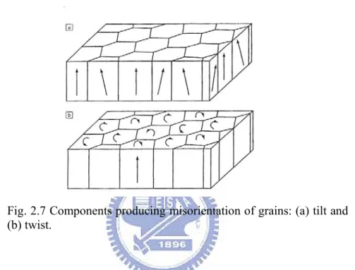
Fig. 2.7 Components producing misorientation of grains: (a) tilt and (b) twist.
The region at the sapphire/film interface has a significant stacking disorder. The stacking sequence may change from abab to cbcb or caca and may be the result of a change from cubic to hexagonal stacking. These threading dislocations are typically pure edge with Burgers vectors and mixed screw edge. Inversion domains may also be formed during initial island growth up to 0.5µm from the interface. Surface pits may be due to island nucleation and the coalescence process. Coalescence is also suggested as the cause for pure-edge dislocations.
25
sapphire. Growth in non-polar directions (m-plane and a-plane) show a greater density of planar defects (stacking faults) being terminated by partial dislocations.
26
Chapter 3 Experimental principles and methods
3.1 Etching process in molten KOH
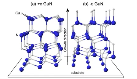
The discrepancy of etching characteristics in Ga-face (+c GaN, Ga-polarity) and
N-face (−c GaN, N-polarity) has been specifically investigated as illustrated in Fig.3.1. Some reports showed that gallium nitride could be etched in the aqueous sodium hydroxide (NaOH) solution but etching ceased when the formation of an insoluble coating of presumably gallium hydroxide (Ga(OH)3) [1, 2]. For further
etching, it would need removing of the coating by continual jet action. All other various aqueous acid and base solutions have been tested for etching of GaN at temperature up to 75oC
were listed in Table 3.1 [3-5]. The undetermined etch rate (nm/min) was because it various from sample to sample and differences in the defect density. According to the research reports in recent years; the common cognition related to gallium nitride etching process was that the most of gallium nitride could be etched rapidly in N-face.
27
Fig. 3.1 Illustration of different polarity, (a) GaN-face (+c GaN, Ga-polarity) (b) N-face (−c GaN, N-polarity)
The reason for the face-dependent gallium nitride etching process has been studied by Li et al., who utilized the X-ray photoelectron spectroscopy (XPS) to examine the surface chemistries before and after etching process in aqueous KOH solutions for both Ga- and N-face gallium nitrides. The conclusion is that the different etching results in Ga- and N-face gallium nitride crystals are due to the different states of surface bonding. Besides, the most important is the etching process only dependent on the polarities, not on the surface morphology, growth condition and which atoms form the surface termination layer. The GaN chemical etching reaction with KOH could be described as the following formula [6]:
3 3 2 KOH 2O Ga O 2NH 3H GaN 2 + ⎯⎯ →⎯ +
28
(Fig.3.2 (d))as well. The mechanism about etching N-face gallium nitride substrate was illustrated in Fig.3.2. The hydroxide ions (OH ) were first adsorbed on the −
gallium nitride surface (Fig.3.2 (b)) and finally react with Ga atoms once the OH −
ions with sufficient kinetic energy as shown in the Fig.3.2(c). The etching could be started at step (c) if the surface was Ga-terminated. The inertness of Ga-face GaN was ascribed to the hydroxide ions would be repelled by the negatively-charged triple dangling bonds of nitrogen near the surface. Thus, if the Ga-face GaN was Ga-terminated, the etching process stops after the first gallium atom layer was removed. In contrast, the N-face GaN, every nitrogen atom with single dangling bond to prevent the hydroxide ions attacking from Ga atoms.
29
Fig.3.2 Schematic diagrams of the cross-section GaN film viewed along the [1120] direction for N-polar GaN to explain the mechanism of the polarity selective etching. (a) Nitrogen terminated layer with one negatively charged dangling bond on each nitrogen atom; (b) adsorption of hydroxide ions; (c) formation of oxides; (d) dissolving the oxides [7].
Table 3.1 All of etching method employed in recent years
Etching solutions GaN etch temperature
Citric acid 75oC Succinic acid 75oC Oxalic acids 75oC Nitric acid 85oC Phosphoric acid 82oC Hydrochloric acid 80oC Sulfuric acid 82oC Potassium triphosphate 75oC
30
Hydrochloric acid/potassium triphosphate 75oC
Boric acid 75oC
Nitric/boric acid 75oC
Potassium tetra borate 75oC
Sodium tetra borate 75oC
Potassium triphosphate 75oC
3.2 Scanning electron microscope and Cathodoluminescence (SEM-CL)
The electron microscope uses electromagnetic lenses to focus the beam to produce an image. However, SEM and TEM differ in the way images are produced and magnified. SEM is used to view the surface or near surface of a sample, whereas TEM provides information of the internal structure of thin specimens. The scanning electron microscope as the name suggests scans across the specimen by the scan coils.
31
As the sample is scanned by the electron beam as shown in Fig. 3.4, it emits electrons and electromagnetic radiation. A detector counts the low energy secondary electrons (< 50 eV) or other radiation emitted. The image is produced by two dimensional intensity distributions by scanning a cathode ray tube (CRT) spot onto a screen and modulating the brightness by the amplified current from the detector. Three dimensional samples change the way electrons are emitted and results in the appearance of a three dimensional image. Resolutions less than 1 nm may be achieved.
3.3 Atomic Force Microscopy (AFM)
The atomic force microscope (AFM) or scanning force microscope (SFM) was invented in 1986 by Binnig, Quate and Gerber. Like all other scanning probe microscopes, the AFM utilizes a sharp probe moving over the surface of a sample in a raster scan. In the case of the AFM, the probe is a tip on the end of a cantilever which bends in response to the force between the tip and the sample. The small probe-sample separation (on the order of the instrument's resolution) makes it possible to take measurements over a small area. To acquire an image the microscope raster-scans the probe over the sample while measuring the local property in question.
32
The resulting image resembles an image on a television screen in that both consist of many rows or lines of information placed one above the other. Unlike traditional microscopes, scanned-probe systems do not use lenses, so the size of the probe rather than diffraction effect generally limits their resolution.
As shown in Fig. 3.5. AFM operates by measuring attractive or repulsive forces between a tip and the sample. In its repulsive "contact" mode, the instrument lightly touches a tip at the end of a leaf spring or "cantilever" to the sample. As a raster-scan drags the tip over the sample, some sort of detection apparatus measures the vertical deflection of the cantilever, which indicates the local sample height. Thus, in contact mode the AFM measures hard-sphere repulsion forces between the tip and sample. In tapping mode, the AFM derives topographic images from measurements of attractive forces; the tip does not touch the sample.
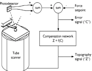
The presence of a feedback loop is one of the subtler differences between AFMs and older stylus-based instruments such as record players and stylus profilometers. The AFM not only measures the force on the sample but also regulates it, allowing acquisition of images at very low forces. As shown in Fig. 3.6, the feedback loop consists of the tube scanner that controls the height of the entire sample; the cantilever and optical lever, which measures the local height of the sample; and a
33
feedback circuit that attempts to keep the cantilever deflection constant by adjusting the voltage applied to the scanner. One point of interest: the faster the feedback loop can correct deviations of the cantilever deflection, the faster the AFM can acquire images; therefore, a well-constructed feedback loop is essential to microscope performance. AFM feedback loops tend to have a bandwidth of about 10 kHz, resulting in image acquisition time of about one minute.
Fig. 3.5 Concept of AFM and the optical lever: (a) a cantilever touching a sample, (b) illustration of the meaning of "spring constant" as applied to cantilevers, (c) the optical lever. Scale drawing; the tube scanner measures 24 mm in diameter, while the cantilever is 100 µm long typically.
34
Fig. 3.6 The AFM feedback loop. A compensation network monitors the cantilever deflection and keeps it constant by adjusting the height of the sample (or cantilever).
3.4 Transmission electron microscope (TEM)
TEM is a method of imaging where a beam of electrons are directed through a sample after which they are scattered into discrete diffracted beams. The diffracted electron beams are then focused in the back focal plane of the objective lens. TEM may have two modes. When operated in diffraction mode, the diffraction lens is focused on the back focal plane to produce a diffraction pattern. For the imaging mode, the diffraction lens is focused on the first image plane to produce a magnified image. In addition, the beam may be allowed to pass through the sample to obtain a bright-field image however the diffracted beams produce a dark-field image.
35
Fig. 3.7 Ray diagram showing two basic operations of TEM
The ray diagram (Fig. 3.7) shows (a) imaging projecting a diffraction pattern and (b) projection of an image onto a viewing screen. The interaction of the electron beam with crystalline material tends to be by diffraction. The orientation of the planes of atoms in the crystal to the electron beam changes the intensity of diffraction. TEM equipment often uses a goniometer to allow the sample to be tilted to a range of angles to obtain specific diffraction conditions. Diffracted electrons are also selected using different apertures. The intensity of diffraction is a maximum at the Bragg angle, although a variation of diffraction intensity occurs with deviation from the Bragg angle. This also depends on the thickness of the specimen. The
36
thinner the crystal sample, the further the crystal may deviate from the Bragg condition.
When crystal planes are almost parallel to the electron beam they are close to fulfilling Bragg’s Law. The majority of electrons are diffracted when the electron beam strikes one set of lattice planes exactly at their Bragg angle and only a few will pass through the sample undeviated. If the planes are exactly at the Bragg condition, strong diffraction will occur and the bright field image will appear dark. This variation with diffraction is shown with bend contours which are a feature of bending of the crystal planes. Dark contour images correspond to regions at the Bragg angle, while light contours result in the regions not strongly diffracting.
3.5 X-ray diffraction (XRD)
X-rays are a form of electromagnetic radiation with a wavelength range from 10 to 0.01 nanometers. The wavelength must be smaller that the atomic spacing of the material being analyzed. The x-rays are created from an electron beam striking a target. The beam should be monochromatic with a very small divergence obtained by collimation.
37
Fig.3.8 Bragg diffraction from a symmetric plane.
X-rays scatter from atoms by different degrees which are dependent on the atom type. However for a good quality x-ray beam incident on a well ordered crystalline material (such as a single crystal semiconductor) the scattered x-rays interfere with each other and result in a diffracted beam leaving the material. This type of diffraction is caused by parallel planes of atoms, in the same way that light may be diffracted by a diffraction grating. For any given values of x-ray wavelength and angle of incidence of the x-ray beam only one set of parallel planes will cause diffraction. This is formalized in Bragg’s Law which states:
nλ=2dsinθ
Where n is an integer value, 1, 2, 3 etc., λ is the wavelength of the x-ray beam, ‘d’ is the lattice constant, the spacing between adjacent parallel planes and ‘θ’ is the angle to the normal of the plane at which the x-ray beam is incident. The diffracted beam leaves the crystal plane at the same angle from the plane’s normal as the
38
incident beam, but in the opposite direction, as can be seen in the Fig. 3.8. It shows a ‘symmetric reflection’, so called because the diffracting plane is parallel to the surface of the crystal. This is the case for diffraction from the 004 plane of a standard orientation (surface is the 001 plane) semiconductor wafer.
Figure 3.9 shows an ‘asymmetric reflection’, in which the diffracting plane is not parallel to the surface of the crystal.
Fig.3.9 Bragg diffraction from an asymmetric plane.
If the same x-ray source and beam conditioner are used then it can be safely assumed that ‘λ’ does not change. Each family of planes within a crystal has a characteristic and unique‘d’ value. It is not possible for diffraction to occur from more than one plane if a single good quality (low divergence and approximately monochromatic) x-ray beam is used. Because of this, knowing the orientation of a wafer allows any plane to be chosen as the diffracting plane.
39
small angle as observed in Fig. 3.10, the diffracted intensity should sharply increase from zero and then sharply decrease to zero, as the x-ray beam–crystal angle passes through the Bragg angle,‘θ’. This is commonly displayed on a ‘rocking curve’, which plots the angle at which the crystal is tilted against the intensity of x-rays from the crystal.
Fig. 3.10 Geometry for x-ray rocking curve. The angle movement for the detector is twice that of the sample.
Bragg’s Law above suggests that for a perfect single crystal and a good quality x-ray beam, one sharp peak should be seen only. Even with a perfect beam of x-rays, rocking curves for more complicated structures, such as the multiple quantum well laser will show multiple peaks.
40
3.6 Photoluminescence spectroscopy (PL)
Photoluminescence characterization equipment generally uses the PL method to obtain the wavelength and intensity of the semiconductor material being analyzed. PL is the process of optical absorption of electrons in solids between an initial energy state Ei and a final energy state Ef. Excitation of an electron to Ef will leave Ei
unoccupied creating a hole. Absorption creates electron-hole pairs while luminescence is the process which occurs when electrons in excited states drop to a lower level emitting a photon ħw as shown in Fig. 3.11. The electron–hole recombination creates a photon which is also known as a radiative transition. Direct gap materials are good light emitters and their optical properties are analyzed using this technique.
Eg
41
Photons are absorbed using an excitation source which is typically a laser. The frequency of the source ħwL must be greater than the energy gap Eg. The result is that
electrons are injected into the conduction band and holes into the valence band. Electrons and holes are initially created in higher states within these bands but will rapidly relax to the bottom of their respective bands reaching their lowest energy state. Relaxation occurs by emitting phonons, for energy loses from the higher states, which obeys the conservation laws. The difference in energy between the two bands is Eg which is the energy gap, also known as the band gap. Luminescence occurs
close to the band gap Eg, near k = 0. After excitation, both electrons and holes relax
to their lowest energy states by emitting phonons.
3.7 Electroluminescence spectroscopy (EL)
As shown in Fig. 3.12, Electroluminescence (EL) is an optical phenomenon and electrical phenomenon in which a material emits light in response to an electric current passed through it, or to a strong electric field. This is distinct from light emission resulting from heat (incandescence), chemical reaction (chemiluminescence), sound (sonoluminescence), or other mechanical action (mechanoluminescence).
42
in a material (usually a semiconductor). The excited electrons release their energy as photons - light. Prior to recombination, electrons and holes are separated either as a result of doping of the material to form a p-n junction (in semiconductor electroluminescent devices such as LEDs), or through excitation by impact of high-energy electrons accelerated by a strong electric field (as with the phosphors in electroluminescent displays).
Fig. 3.12 Spectrum of a blue/green electroluminescent light source for a clock radio (similar to the one seen in the above image). Peak wavelength is at 492 nanometers and the FWHM spectral bandwidth is quite wide at about 85 nm.
3.8 Reference
43
[2] J.I. Pankove, J. Electrochem. Soc. 119, 1118 (1972).
[3]H. Cho, D.C. Hays, C.B. Vartuli, S.J. Pearton, C.R. Abernathy, J.D. MacKenzie, F. Ren, J.C. Zolper, Mater. Res. Soc. Symp. Proc. 483, 265 (1998).
[4] C.B. Vartuli, S.J. Pearton, C.R. Abernathy, J.D. MacKenzie, F. Ren, J.C. Zolper, R.J. Shul, Solid-State Electron. 41 (12), 1947 (1998).
[5] S.J. Pearton, R.J. Shul, Gallium nitride I, in: J. Pankove, T.D. Moustakas (Eds.), Semiconductor and Semimetals Series, vol. 50, Academic Press, New York, NY, p. 103 (1998).
[6] D. Li, M. Sumiya, S. Fuke, D. Yang, D. Que, Y. Suzuki, Y. Fukuda, J. Appl. Phys. 90, 4219 (2001).
[7] D. Li, M. Sumiya, K. Yoshimura, Y. Suzuki, Y. Fukuda, S. Fuke, Phys. Status Solidi A 180, 357 (2000).
44
Chapter 4 Analysis of UVLED regrown on HIP-GaN substrate
4.1 Fabrication of UV LED epitaxial structure
The material epitaxial growth uses nominal low pressure metalorganic chemical vapor deposition (MOCVD). A 30 nm of low temperature (LT) GaN nucleation layer followed by a 2.5 µm GaN buffer layer was grown on (0001) sapphire template. The GaN wafer with HIP structure was etched by high temperature molten KOH at 280oC for 12 minutes, in contrast, the reference sample without doing any process. Inverted micro pyramid structures were formed at the GaN-sapphire interface. The LED device structure was 3.5 um n-doped GaN, 10 pairs of Al0.05Ga0.95N/InGaN quantum
wells (13nm/2.5nm), and 30 nm of p-doped AlGaN cap layer.
The designed quantum well wavelength was at 394 nm. This shorter wavelength, as opposed to the more frequently used 450 nm LED wavelength, was chosen mainly to test the material quality because PL efficiency is much more sensitive to defects at shorter wavelength [1].
4.1.1 Process flow of HIP-structure LED
It is very interesting to note that the regrowth step did not fill up the space and the inverted pyramid structures at the GaN-sapphire interface. A cross section SEM image of a cleaved sample after regrowth process is shown in Fig. 4.1(a). The
45
inverted pyramid structures pretty much extended through out very large area as shown in the zoom out Fig. 4.1(b). Some of the pyramid tips are still in contact with sapphire while some are completely detached from sapphire. To investigate the performance of the new device structure and make fair comparisons, a reference wafer also went through exactly the same growth processes except skipping the KOH etching step.
58ל Mesa
(a) (b)
Fig. 4.1 (a) SEM cross section image of the regrown sample. (b) A zoom out view of the inverted pyramid structures at GaN-sapphire interface.
Indium–tin oxide (ITO) and Ni/Au were subsequently evaporated onto the sample surface to serve as p-type electrode. Ti/Al/Ni/Au contact was deposited onto the exposed n-GaN layer to serve as the n-type electrode. Finally, the epitaxial wafers were lapped down and then scribed to the fabrication of 350×350 µm2 UVLEDs. The
46 4.2(a)-(c).
(a)
(b)
(c)
Sapphire u-GaN Sapphire u-GaN Sapphire u-GaN ITO p-GaN n-GaN 10 pairs of MQWsFig. 4.2 The process flow of UV HIP-LED with inversed pyramid GaN/air
47
4.2 Material properties analysis
4.2.1 Surface morphology analysis of HIP structure
In Fig. 4.3, we could observe the surface morphology after wet etching process by molten KOH. There were many dark points as shown in position A, which represents the hydroxide ions (OH
) have totally attacking the Ga atoms along the dangling bond of threading dislocations to the sapphire substrate [2]. It is obvious most of threading dislocations could be etched and results in enormous of hexagonal pits on the u-GaN surface as indicated in position B. After 12 minutes later, the u-GaN remained on sapphire as region could be regarded as defects-free GaN seed for regrowth afterward. As etching time increased, few hexagonal pits would be extend and combine together. Therefore, there were few regions as position C for regrowth main mesas.
A
B
C
48
The observation of local region on high resolution and 45 view angle by SEM o
could be shown in Fig. 4.4. In region D (dashed square), the remained GaN mesas with different depth after few pits combine together. Because of different growth rate between inner sidewalls and mesas, partial coalesce dislocation could be annihilated or bent by lateral overgrowth under the etched pits. As mentioned before, the KOH solution would etch down to the GaN/sapphire interface then etch back the Ga-face in reverse direction. When pits further extended, it was possible for GaN separate from sapphire substrate as shown in middle of Fig.4.4. The arrow (region E) points out the hexagonal inverted-pyramid (HIP), which was the evidence of hydroxide ions attack Ga-polar easily.
E D
Fig. 4.4 Enlarge local region of the etching pits SEM image
4.2.2 Roughness analysis by AFM after LED regrowth
49
regrowth on HIP GaN substrate as shown in Fig. 4.5. The root mean square (rms.) value of flatness was 0.924 nm, which demonstrates the HIP structure, would not be destroyed the flatness of UVLED.
Digital Instruments NanoScope Scan size 5.000 µm Scan rate 1.001 Hz Number of samples 256 Image Data Height Data scale 10.00 nm Img. Rms 0.924 nm
Height
Fig. 4.5 AFM analysis after UVLED regrowth
4.2.3 X-ray diffraction analysis
The X-ray diffraction (XRD) rocking curves of these two samples are shown in Fig. 4.6. The linewidth for (102) planes was reduced from 552 to 472 arcseconds. The linewidth for (002) planes was only reduced from 338 to 335 arcseconds. It has been reported that the XRD linewidthes for (102) and (002) planes are respectively related to edge and screw threading dislocation densities [3]. The significant decreases in XRD linewidthes indicate a reduction in threading dislocation density. The improvement in crystal quality is attributed to the strain relaxation of the partially
50
relieved GaN layer in combination with the subsequent regrowth. When the initial GaN epitaxial layer was grown on sapphire, a compressive strain was built up inside the material due the mismatched lattice constants and thermal expansion coefficients between GaN and sapphire. These mismatched factors introduced various threading dislocations. The KOH etching partially relieved GaN from sapphire interface and relaxed the compressive strain. This partially relieved layer served as a template for subsequent regrowth process. It acted as a buffer layer to partially filter out the problems of mismatched lattice constant and thermal expansion coefficient for MOCVD growth and resulted in improved crystal quality.
(002)
(102)
Fig. 4.6 X-ray diffraction rocking curves for HIP-LED and Conv.-LED samples.
51
Table 4.1 Analytic data from XRD ω-scan
Substrate 002 102
Conv. GaN 338 552
HIP structure 335 472
4.2.4 Defects formation analysis by TEM
The most general threading dislocations (F region) could be seen in Fig. 4.7. The dashed line indicates the u-GaN and UVLED regrowth interface. The G regions near dashed line exhibited some particular mechanism, which prevent the threading dislocation pass through the multiple quantum well along the growth direction. We could see the dislocation bent and annihilated in G1 position, form stacking fault in
G2 position and loop in G3 position. Besides, we could also see the air void below the
dashed line. It might result from the slower growth rate at inner sidewalls, thus the region would be buried in lateral overgrown GaN. The pointed out I region indicate the GaN/sapphire interface. Because there were a few adhesion areas, it would easily separate from sapphire when preparing the thin LED sample for TEM.
52 F G1 G2 G3 H I 0001 1100
Fig. 4.7 TEM image of HIP structure UVLED
To realize reasons for threading dislocation survived in u-GaN, we enlarge the particular TEM J region as seen in Fig. 4.8. It seems threading dislocation could be protected once the outer sidewalls of GaN pyramid with good crystalline quality as in K regions, thus the hydroxide ions could not attack the atoms with dangle bonds.
J K
K
53
The high resolution TEM image near UVLED multiple quantum wells. There were ten pairs of MQWs and three typical threading dislocations as shown in Fig. 4.9. We could found that the flatness of MQWs would not be destroyed for sample regrowth on GaN substrate with HIP structure.
Fig. 4.9 High resolution TEM image near UVLED MQWs
4.2.5 Model of multi-layers epitaxial overgrowth (ML-ELOG)
To describe the formation of threading dislocation on HIP template, we propose a model named ML-ELOG to support the result in TEM images. The dislocation might be bent, annihilated or forming loops followed the lateral growth direction. At the coalescence region would form new threading dislocations or stacking faults. Therefore, most of dislocation have been etched or even removed after the KOH etching process. As schematic in Fig. 4.10, the ML-ELOG mechanism could
54
effectively prevent the threading dislocation continuous threading through to MQWs region. TDs
GaN/Sapphire interface
undercut u-GaN
substrate
regrowth GaN
air void Bending or annihilationTunnels for KOH 0001
1100
Fig. 4.10 Mechanical of multi-layer epitaxial lateral overgrowth (ML-ELOG)
4.3 Optical properties analysis of UV-LED regrown on HIP
GaN substrate
4.3.1 Photoluminescence spectrum
The room temperature photoluminescence spectrum as observed in Fig. 4.11, we could found the integrated intensity of sample with HIP structure was almost 4.8 times of UV-LED grown on conventional GaN substrate. The full width at height maximum (FWHM) of sample with HIP structure and conventional were 113 meV and 106.3 meV, respectively. The shorter wavelength for UVLED with HIP structure might attribute to the partial strain relaxation in GaN/sapphire interface. The
55
emission peak wavelength of Conv.-LED and HIP-LED were 393.35 and 398.19nm, respectively. It was known that the magnificent lattice mismatch between GaN and sapphire would induce large compressive stress. Thus, the reason for the HIP-structure with smaller bandgap might attribute to the partial stress relaxation the interface. 300 350 400 450 500 0.0 2.0x10⁵ 4.0x10⁵
Lu
min
escen
ce int
en
sit
y (
a
rb. un
it
)
Wavelength (nm)
HIP structure Conv. GaN substratePL temperature : 300 K
Fig. 4.11 Room-temperature photoluminescence spectrum
Table 4.2 Analytic data in PL spectrum Substrate Peak energy (eV) Integrated intensity (a.u.) Wavelength (nm) FWHM (meV)
Conv. GaN 3.15 1.2E4 393.35 106.3
56
4.3.2 Far-field optical pattern
We also measure the three-dimension far field pattern of HIP-LED and Conv.-LED at a 20 mA operating currents as show in the Fig. 4.12(a). It could be obviously observed that the HIP-LED emission intensity have better distribution in the normal direction. This was suggesting that the guiding light (excess the total reflective angular) in GaN would be redirected by reflection in the HIP GaN/air interface with high difference refractive index. As show in Fig. 4.12(b), the divergent angle of HIP-LED and Conv.-LED were calculated to be 108 and 128 degree from the normalized 2D radiation pattern.
HIP structure Con. GaN structure
57 (b)
Fig. 4.12 (a) 3D far field pattern of HIP-LED and Conv. LED (b) divergent angle of samples calculated to be 108 and 128 degree from the normalized 2D radiation pattern.
4.3.3 TracePro geometrical optics simulation
The ray tracing simulations are shown in Fig. 4.13(a)-(c) to investigate the effect of the micro pyramid structures at GaN-sapphire interface. The reflection coating at sapphire back surface is included in simulation. The sub bandgap absorption coefficient for GaN is assumed to be 1 cm-1 [5]. The quantum well re-absorption coefficient is assumed to be 10 cm-1. These numbers varies depending on samples
and are very coarse estimates here mainly to facilitate simulation and see the general feature. Figure 4.13(a) and (b) were the zoom in pictures to show the rays near GaN-sapphire interface. It shows that there is less light entering sapphire substrate for HIP-LED compared to Conv.-LED. The inverted pyramid structures help to redirect the radiation toward sapphire substrate to the front surface direction. Figure
58
4.13(c) and (d) were the full views of ray tracing. It clearly demonstrates that the light output coupling was greatly enhanced and mostly coupled out in the normal direction. n-GaN/MQWs n-GaN Sapphire Inverted Pyramids n-GaN/MQWs n-GaN Sapphire Inverted Pyramids Sapphire n-GaN p-GaN/MQWs Sapphire n-GaN p-GaN/MQWs (a) (b)
p-GaN/MQWs/
n-GaN/
Inv. Pyramids
Sapphire
Al mirror
p-GaN/MQWs/
n-GaN/
Inv. Pyramids
Sapphire
Al mirror
p-GaN/MQWs/
n-GaN/
Sapphire
Al mirror
p-GaN/MQWs/
n-GaN/
Sapphire
Al mirror
(c) (d)Fig. 4.13 Ray tracing simulations. (a) and (b) are zoom in views at GaN-sapphire interface for HIP-LED and Conv.-LED. (c) and (d) are full chip views. Light is effectively coupled out in normal direction for HIP-LED.
59
4.4 Electrical properties analysis of UVLED regrown on HIP
GaN substrate
4.4.1 Electroluminescence spectrum
The electroluminescence (EL) spectra of both LEDs, collected in the normal to the front surface direction, are shown in Fig. 4.14. The integrated EL power of HIP-LED is enhanced by 120% compared to that of Conv.-LED. The EL spectrum of Conv.-LED shows slight Fabry-Perot mode ripples. The Fabry-Perot modes are formed by the top GaN-air and bottom GaN-sapphire interfaces. The Fabry-Perot mode spacing is about 5 nm, which is consistent with the overall thickness of 6 µm and GaN refractive index of 2.55 at 394 nm. The EL spectrum of HIP-LED on the other hand does not have the same Fabry-Perot mode ripples. This is because the randomly distributed surfaces of micro pyramid structures suppress the standing wave formation between the top and bottom interfaces. As a result, its spectrum does not show visible Fabry-Perot ripples. It is also worth to note that the peak wavelength of HIP-LED was red shifted by 2 nm compared to that of Conv.-LED. It has been reported that a compressive strain introduces a blue shift in the band edge emission wavelength [4]. The red shift in peak emission indicates the relaxation of the compressive strain in HIP-LED.
60 380 400 420 440 0.0 4.0x10⁴ 8.0x10⁴ 1.2x10⁵
Integ
ra
ted i
n
te
nsi
ty (ar
b
. uni
ts)
Wavelength (nm)
HIP structure Conv. GaN substrate EL temperature : 300 K Injection current @ 20mAFig. 4.14 HIP-LED and Conv.-LED EL spectra measured in normal direction
4.4.2 Current-dependent EL intensity
The observation of current-dependent electroluminescence has been investigated in this study. As shown in Fig. 4.15, the current-dependent spectra of HIP structure and conventional GaN substrate could seen the integrated intensity droop at 170 mA and 190 mA, respectively. It may attribute to the HIP structure suffer from worse heat sink at high injection current.
61 0 50 100 150 200 250 0 10 20 30 40 50
Injection current (mA)
Output powe
r (mW
)
HIP sturcture Conv. GaN substrate
Fig. 4.15 Integrated intensity versus injection current
4.4.3 L-I-V characteristic curve analysis
The light-current (L-I) and voltage-current (V-I) characteristics are shown in Fig. 4.16. The forward voltages of HIP-LED and Conv-LED were respectively 3.86 and 3.80 V at 20 mA. The voltages increase to 5.09 and 4.93 V at 100 mA. The electric characteristic of HIP-LED was still reasonably well maintained after chemical etching and regrowth processes. The optical power was collected by an integrating sphere to make sure that radiation in all directions was collected. The total optical output powers of HIP-LED and Conv.-LED were 3.95 and 7.31 mW respectively at 20 mA and 23.7 and 37.5 mW at 100 mA. Compared to Conv.-LED and HIP-LED, the out power exhibits 85% and 58% enhancement at 20 and 100 mA, respectively.
62
The L-I curves of both samples are still fairly linear up to 100 mA injection current. The decrease of output power enhancement from 85% to 58% is likely due to the less effective thermal dissipation provided by the small contacts of the inverted pyramids at sapphire interface.
0
20
40
60
80
100
0
2
4
6
Voltage (eV)
HIP structure Conv. GaN substrate0
10
20
30
40
Output power (mW)
Forward injection current (mA)
Fig. 4.16 L-I-V curves of HIP-LED and Conv.-LED.
4.4.4 Observation of Leakage current
To examine the leakage current of both UV LED devices under reverse bias voltage. As observed in Fig. 4.17, the leakage current of Conv.-LED and HIP-LED were 7.2 nA and 1.4 nA at -5 V, respectively. The much smaller leakage current might induced from better crystal quality for UVLED regrowth on substrate with HIP structure. It was corresponding to what we expect in TEM images result and ML-ELOG model.
63 -6 -4 -2 0 2 4 6 1E-10 1E-8 1E-6 1E-4 0.01
Cu
rrent (A)
Bias voltage (V)
HIP structrue Conv. GaN substrateFig. 4.17 Leakage current of HIP structure and Conv. GaN UVLED under reverse bias
4.5 Reference
[1] Asif Khan, Krishnan Balakrishnan and Tom Katona, Nature Photonics 2, 77 - 84 (2008).
[2] D. Li, M. Sumiya, K. Yoshimura, Y. Suzuki, Y. Fukuda, S. Fuke, Phys. Status Solidi A 180, 357 (2000).
[3] H. Heinke, V. Kirchner, S. Einfeldt, and D. Hommel, Appl. Phys. Lett. 77, 2145 (2000).
[4] P. P. Paskov, R. Schifano, T. Malinauskas, T. Paskova, J. P. Bergman, B. Monemar, S. Figge, D. Hommel, B. A. Haskell, P. T. Fini, J. S. Speck, and S. Nakamura, phys. stat. sol. (c) 3, No. 6, 1499-1502 (2006)
64
[5] W. Rieger, R. Dimitrov, D. Brunner, E. Rohrer, O. Ambacher, and M. Stutzmann, Phys. Rev. B, 54, 17596 (1996)
65
Chapter 5 Mechanical lift-off by HIP-structure
5.1 Mechanical lift-off process flowchart
The GaN based LED structures were grown on HIP GaN/air template by lateral re-growth process. After Ni/Au p-GaN contact layer was deposited on the p-GaN layer by the E-gun process, which was followed by a 2 min annealing process to achieve a low-resistance contact. The annealing temperature was 500 °C in ambient air. After annealing process, a reflective layer of 1500 Å Al was deposited to prevent light from reaching the absorbing Si substrate. Then, a metalized Ni/Au bonding layer was deposited on the top of the Al layer. The thicknesses of Ni and Au layers were 1500 and 2000 Å, respectively. This 1500 Å Ni layer serves as an adhesive barrier layer and the 2000 Å Au layer serves as the seed layer for the electroplating process of 5 µm thick Au layer used to do Au-Si wafer bonding.
In Au-Si wafer bonding process, GaN thin film with HIP structure and sapphire substrate were under 400 °C. GaN the GaN based LED structures were grown on HIP GaN/air template by lateral re-growth process. After Ni/Au p-GaN contact layer was deposited on the p-GaN layer by the E-gun deposition system, which was followed by a 2 min annealing process to achieve a low-resistance contact. The annealing temperature was 500 °C in ambient air. After annealing process, a
![Fig. 1.5 The schematic illustration of the proposed mechanism involved in the GaN [16]](https://thumb-ap.123doks.com/thumbv2/9libinfo/8256344.171900/17.892.264.632.267.436/fig-schematic-illustration-proposed-mechanism-involved-gan.webp)
![Fig. 1.7 Cross-sectional TEM image of the GaN layer grown on patterned-sapphire substrate [18]](https://thumb-ap.123doks.com/thumbv2/9libinfo/8256344.171900/19.892.273.625.161.415/cross-sectional-image-layer-grown-patterned-sapphire-substrate.webp)
![Fig. 1.8 Schematic dislocation reduction models of three different island and facet formation of FC-GaN: (a) small island size, (b) horizontal plane formed on the islands and (c) optimized island size and { 10 1 1 } facet formation [19]](https://thumb-ap.123doks.com/thumbv2/9libinfo/8256344.171900/20.892.329.597.525.915/schematic-dislocation-reduction-different-formation-horizontal-optimized-formation.webp)