國 立 交 通 大 學
光電工程研究所
博 士 論 文
飛秒雷射退火:
再結晶、控制佈植活化深度及薄膜電晶體製作的新技術
Femtosecond laser annealing:
a novel approach for recrystallization, dopant profile engineering and
fabrication of Thin Film Transistors
研究生:王怡超
指導教授:潘犀靈 教授
飛秒雷射退火:
再結晶、控制佈植活化深度及薄膜電晶體製作的新技術
Femtosecond laser annealing:
a novel approach for recrystallization, dopant profile engineering and fabrication of Thin Film
Transistors
研 究 生:王怡超 Student:Yi-Chao Wang
指導教授:潘犀靈 教授 Advisor:Prof. Ci-Ling Pan
國 立 交 通 大 學
光 電 工 程 研 究 所
博 士 論 文
A Thesis
Submitted to Department of Photonics & Institute of Electro-Optical Engineering
College of Electrical Engineering National Chiao Tung University In partial Fulfillment of the Requirements
for the Degree of Doctor of Philosophy
in
Electro-Optical Engineering
December 2007
Hsinchu, Taiwan, Republic of China
中華民國九十六年十二月
飛秒雷射退火:
再結晶、控制佈植活化深度及薄膜電晶體製作的新技術
學生:王怡超
指導教授:潘犀靈 教授
國立交通大學光電工程研究所 博士班
摘
要
本論文之主要內容可分為三個部分。首先是利用飛秒雷射進行非
晶矽退火的研究並將此一新技術應用於複晶矽薄膜電晶體(TFT)的製
作,其次是利用飛秒雷射在矽及鍺基板上進行超淺介面佈植活化的研
究,最後則是利用兆赫波時域解析技術研究飛秒雷射退火非晶矽並藉
此辨別退火後複晶矽的結晶特性。
傳統的非晶矽退火主要是利用爐管及準分子雷射進行。然而爐管
退火必須在
550 ℃進行,因而限制其在玻璃基板上的應用。非晶矽在
一般準分子雷射波段(λ=248-308 nm)的線性吸收係數雖然大約是近紅
外飛秒雷射波段(λ=800 nm)的兩千倍,但是近紅外飛秒雷射退火所需
要的能量密度卻更低(~50 mJ/cm
2)。研究中發現照射適當數量的飛秒
雷射脈衝可以得到最大的晶粒尺寸約
800 nm,且退火樣品的表面平
整度極佳(RMS roughness <10 nm)。將飛秒雷射退火複晶矽應用於
TFT製作可以證實此一技術實際應用的可能性。飛秒雷射退火在小長
寬比(2μm/2μm)TFT可得到最佳的載子遷移率約 160 cm
2/Vs,同時藉
由field-effect-conductance的方式分析元件的缺陷密度。這兩項與準分
子雷射退火複晶矽TFT極為接近的關鍵特性皆說明了飛秒雷射退火
未來應用的潛力。
為了克服元件尺寸減小時造成的短通道效應,超淺介面佈植活
化在高速元件例如金氧半場效電晶體(MOSFET)的製作上極為重要。
在快速升溫退火及準分子雷射活化技術逐漸成熟的同時,準分子雷射
的熱致熔融與快速升溫退火活化在硼或磷原子活化時仍然會造成約
數十奈米的擴散。藉由超短脈衝雷射活化所造成的非熱熔融,活化過
程中僅造成佈植原子極微小的擴散(~ 10 nm)。不僅可將片電阻降低到
100-400 Ω/,且佈植原子的活化效率約可達到 28-35%,同時熱致熔
融所常見的佈植原子散逸也得到避免。超短脈衝雷射活化應用在鍺基
板上亦可得到極佳的活化效果。
複晶矽的晶粒尺寸是製作
TFT 時的重要參數,因為其與 TFT 載
子遷移率有極大的關聯。但是觀察晶粒尺寸屬於破壞性的量測,因為
必須先將退火後的複晶矽作蝕刻再以電子顯微鏡觀察晶粒。利用光激
發-兆赫波探測的方式可以在不損壞樣品的前提之下觀察不同晶粒尺
寸樣品的折射率以及導電率隨時間的變化,並藉由兆赫波時域解析的
量測得到其光激載子的遷移率。
Femtosecond laser annealing:
a novel approach for recrystallization, dopant profile engineering and
fabrication of Thin Film Transistors
Student:Yi-Chao Wang
Advisors:Dr. Ci-Ling Pan
Institute of Electro-Optical Engineering
National Chiao Tung University
ABSTRACT
The main topics of this thesis can be divided into three categories; (1) near-infrared femtosecond laser-induced crystallization of amorphous silicon and the performance of thin film transistors (TFTs) annealed by this technique; (2) dopant profile engineering by near–infrared femtosecond laser activation (FLA) on Si and Ge substrates; (3) time-resloved THz spectroscopy of femtosecond-laser-annealed amorphous silicon for grain quality diagnosis.
Polycrystalline silicon (poly-Si) can be obtained by furnace annealing and excimer laser annealing (ELA) applied on amorphous silicon (a-Si). However, the process temperature of furnace annealing is 550 ℃, which may induce the melting of glass substrate. The linear absorption coefficient of a-Si at the wavelength from 248 to 308 nm is two thousand times higher than that at a wavelength of 800 nm. FLA is still able to anneal a-Si in a fluence about 50 mJ/cm2, which is lower than ELA process. The largest average grain size obtained by irradiates a-Si with appropriate number of laser pulses is about 800 nm. This is accompanied with good surface roughness (RMS roughness < 10 nm). Polycrystalline silicon processed by FLA is applied on TFT fabrication and a highest mobility of 160 cm2/Vs is obtained. The highest mobility and trap state density of FLA processed TFTs is similar to that of ELA processed TFTs. This also approved the potential of FLA on TFT fabrication.
the lateral and vertical diffusion of the device’s junction is necessary to prevent short channel effect. Thus ultrashallow and highly activated junctions are essential for metal-oxide-semiconductor field effect transistor production. Although rapid thermal activation and ELA already being studied and approved to be effective technique on dopant activation, dopant diffusion in several tens of nanometer is still observable. Irradiated by femtosecond pulses, structural change can occur while the electronic systems of the lattice are not in thermal equilibrium with each other. Such a non-thermal melting mechanism could minimize dopant diffusion (~ 10 nm) significantly by reducing the thermal budget of activation. The measured sheet resistance and activation efficiencies of ion-implanted samples were in the range of 100-400Ω/ and 28-35% respectively. Dopant loss which is frequently observed in thermal activation is also improved quite substantially. Ultrafast laser activation on Ge substrate also shows good performances.
Grain size of poly-Si is very important because it correlates with the mobility of TFT. Traditionally, the grain size is examined by scanning electron microscopy. However, Secco etching is required for sample preparation of SEM, which may cause damages on the sample. By using optical-pump–THz-probe (OPTP) technique we can measure the temporal evolution of far-infrared conductivity and refractive index which is induced by the optical pump beam. We can also examine the carrier mobility of FLA-processed poly-Si by OPTP technique.
Acknowledgement (致 謝)
博士班的研究生涯終於告一段落。首先我要感謝潘老師這幾年來
的耐心指導,讓我在研究的路上能排除困難達成目標。同時也感謝國
家奈米元件實驗室的謝博士對於研究方向以及實驗設備的大力支
持。我也要感謝安惠榮老師及冉曉雯老師在實驗上給我的指導及幫
助。此外也感謝所有的好朋友們以及在實驗室中與我一起努力的夥伴
們,你們的支持是我在遭遇挫折時的最大支柱。
感謝我的父母及家人們在我求學的這些年對我的支持以及包容,
讓我能無後顧之憂的專注於研究。也感謝朋友們的支持及協助,希望
能與你們一起分享完成這篇論文的喜悅。
怡超 2007/12/26
Table of Contents
中文摘要………
i
Abstract………
iii
Acknowledgement (致謝)………
v
Table of Contents………
vi
List of Figures………
ix
Table Lists
………
xiii
Chapter 1 Introduction……….1
1.1 Introduction of Low Temperature Poly-Si TFTs………1
1.2 Crystallizaiton of Amorphous Silicon (a-Si) Thin Films………2
1.2.1 Solid Phase Crystallization………3
1.2.2 Excimer Laser Crystallization………3
1.3 Dopant Profile Engineering of Ion-Implanted Semiconductors………..5
1.3.1 Rapid Thermal Activation………..6
1.3.2 Excimer Laser Activation………...6
1.4 Time-Resolved Teraherz Spectroscopy………...7
1.5 Motivation………...………8
1.6 Organization of thesis………..……….….10
References……….……….11
Figures………16
Chapter 2 Femtosecond Laser Crystallization of Amorphous Silicon Thin Films and Characterizations of Crystallized Polycrystalline Silicon Thin Film Transistors………...19
2.1 Introduction………..….19
2.2 General Features of Femtosecond Lasers……….20
2.3 Experiment setup and procedures……….21
2.3.1 The Setup of Femtosecond Laser Crystallization and Sample Preparation………21
2.4 Results and Discussions………...…….22
2.4.1 Material Characterization of Femtosecond Laser Crystallized Poly-Si Thin Films………..………..22
2.4.2 Electrical Characterization of TFTs Fabricated by Femtosecond Laser Crystallization………..26
2.5 Summary………...………28
References………..30
Figures………33
Tables………...………..42
Chapter 3 Dopant Profile Engineering by Near-Infrared Femtosecond Laser Activation………..…………43
3.1 Introduction………...………43
3.2 Experiments setup and procedures………44
3.3 Results and Discussions………...…….45
3.3.1 Material Characterization of Femtosecond Laser Activated Si……...45
3.3.1.1 Secondary Ion Mass Spectroscopy Analysis………45
3.3.1.2 Electrical Characterization of Femtosecond Laser Activated Si…..48
3.3.2 Material Characterization of Femtosecond Laser Activated Ge……..49
3.3.2.1 Secondary Ion Mass Spectroscopy Analysis………49
3.3.2.2 Electrical Characterization of Femtosecond Laser Activated Ge….51 3.4 Summary………...52
References………..54
Figures………58
Tables………...………..64
Chapter 4 Time-Resolved THz Spectroscopy of Femtosecond-Laser-Annealed Amorphous Silicon………...66
4.1 Introduction………...……66
4.2 Generation and Detection of Terahertz Radiation………67
4.2.1.1 Surface Depletion Field………....67
4.2.1.2 Photo-Dember Effect………....68
4.2.2 Free Space Electro-Optics Sampling………...70
4.3 Experiments………..71
4.3.1 Terahertz Time Domain Spectroscopy………71
4.3.2 Optical-Pump-Terahertz-Probe System………...…72
4.4 Extraction of Optical Constant by Terahertz Time Domain Spectroscopy..74
4.5 Determination of Mobility and Conductivity from Drude Model…………76
4.6 Results and Discussions………76
4.6.1 Optical-Pump-Terahertz-Probe Measurements………..…..77
4.6.2 Terahertz Time Domain Spectroscopy Measurements………...…….78
4.7 Summary………...………81
References………..83
Figures………87
Tables………...………..95
List of Figures
Chapter 1Fig.1-1. Grain size and corresponding poly-Si TFT mobility vs. laser fluence for conventional ELA process………....16 Fig.1-2. SLG growth initiates from the seeds, which survived in the melting process, at the Si-SiO2 interface……….16
Fig.1-3. SIMS profiles of a 20 keV BF2 2×10¹⁵/cm2 before and after annealing. The
annealing process was performed by RTA or ELA………...………..17 Fig.1-4. Comparison of boron concentration profiles after laser annealing with successive pulses at 1 J/cm2……….17 Fig.1-5. Electromagnetic spectrum of THz……….…………..18 Fig.1-6 The wavelength dependence of linear absorption coefficient for silicon………..…….18
Chapter 2
Fig.2-1. Block diagram of the laser system for FLA experiment……….33 Fig.2-2. The chirped amplification process of regenerative Ti:Sapphire amplifier system………...…33 Fig.2-3. Experimental setup of FLA………… ………...……….34 Fig.2-4. Vacuum chamber and tow axis transition stage of FLA experiment… ….34 Fig.2-5. Sketch map of line-scan FLA……… …….35 Fig.2-6. SEM pictures of FLA pc-Si samples after Secco etching for steady-state (a, b, c, d) and line-scanned FLA (e, f, g, h)……….35 Fig.2-7. Average grain sizes of FLA pc-Si films, irradiated with pulses of different durations, as a function of laser fluence for steady-state FLA and scanned FLA……36 Fig.2-8. Average grain sizes of FLA pc-Si films, irradiated with pulses of different durations, as a function of interpulse overlapping for steady-state FLA and scanned FLA………..………36
Fig.2-9. (a): Raman spectra, and (b, c): AFM images, of FLA pc-Si films irradiated with 50 fs pulses. Line-scan (steady-state) mode is performed using EL of 46 mJ/cm2
(60 mJ/cm2) and overlapping of 95 % (20 laser-shots)………37 Fig.2-10. TEM diffraction patterns of FLA-processed poly-Si films irradiated with 50 fs pulses………37 Fig.2-11. XRD spectra of FLA-processed poly-Si films irradiated with 50 fs pulses.38 Fig.2-12. Maximum average grain size of FLA pc-Si films, and corresponding optimal laser fluence, as a function of substrate temperature………..38 Fig.2-13. Transfer characteristics and transconductance versus gate voltage for FLA and SPC processed TFTs with channel dimensions of (a) W = L= 2 μm and (b) W = L= 10 μm………..………39 Fig.2-14. (a) Threshold voltages, (b) subthreshold slopes and (c) mobilities for TFTs annealed by FLA with different fluences and SPC process………..……...40 Fig.2-15. Transfer characteristics of the sample (W = L = 5 μm) measured at different temperatures………...40 Fig.2-16. Grain trap-state density in the energy bandgap of the FLA and SPC processed TFT with different channel dimensions and fluences in compare with furnace annealed TFT………..……….41
Chapter 3
Fig.3-1. SIMS profiles of as implanted B-doped samples, with (sample A) and without PAI (sample B) as well as BF2+-implanted samples (sample C). SIMS profiles
for all B-doped layers activated by FLA at different substrate temperature are also shown………...…….58 Fig.3-2. SIMS profiles for BF2+-implanted layers activated by either FLA or ELA at
different substrate temperatures. SRP profiles for BF2+-implanted layers activated by
FLA at different temperature are also shown………...………58 Fig.3-3. SIMS and SRP profiles for P-implanted layers activated by FLA at
different substrate temperatures. SIMS profiles for P-implanted layers activated by ELA at different substrate temperatures are also shown. The dopant depth was designed to be the same as for BF2+-implanted samples………..59
Fig.3-4. AFM result of FLA-activated B-implanted Si……….………59 Fig.3-5. AFM result of FLA-activated P-implanted Si………...………..60 Fig.3-6. Sheet resistance of sample C activated with different overlapping of neighboring pulses and different substrate temperature…………...………60 Fig.3-7. Sheet resistance of sample D activated with different overlapping of neighboring pulses and different substrate temperature………..…….61 Fig.3-8. Phosphorous SIMS profiles of the samples annealed with different number of laser pulses. The inset shows the corresponding sheet resistance and mobility of the samples……….………61 Fig.3-9. Phosphorous SIMS profiles of the samples annealed with various laser fluences. The inset shows the corresponding sheet resistance and mobility of the samples……….61 Fig.3-10. Boron SIMS profiles of the samples annealed with various number of laser pulses. The inset shows the corresponding sheet resistance and mobility of the samples……….62 Fig.3-11. Boron SIMS profiles of the samples annealed with various laser fluences. The inset shows the corresponding sheet resistance and mobility of the samples.…..63
Chapter 4
Fig.4-1. Band picture and the schematic flow of drift current in (a) for n-type and (b) for p-type………..………87 Fig.4-2. The schematic flow of diffusion current near the surface of semiconductor which is induced by photoexcited carriers………...…………87 Fig.4-3. The scheme map of the THz-TDS system. BS: beam splitter; B:
polyethylene visible beam block; F: blue filter; WP: Wollaston prism; P: pellicle.…88 Fig.4-4. Sample structure of a-Si and scheme of the OPTP system. BS: beam splitter; B: polyethylene visible beam block; F: blue filter; S: sample; WP: Wollaston prism; P: pellicle……….……….88 Fig.4-5. The scheme of poly-Si and sample mount with 2mm-diameter aperture…89 Fig.4-6 (a) Time domain electric field of THz pulse. (b) Amplitude spectrum for the THz pulse in (a)………89 Fig.4-7. The schematic sample between pump and unpump. n1, n2, n3 is the
refractive indices. E0(ω ) is the incident THz field. Eref(ω ) and Efilm(ω ) are the
reference (without pump) and sample (with pump)……….90 Fig.4-8. SEM pictures of pc-Si samples annealed by FLA with (a) 45, (b) 34
mJ/cm2………..90
Fig.4-9. Differential transmission at the peak of the THz pulse for different grain sizes of poly-Si……….91 Fig.4-10. The experimental results and fitting results of n and к of (a) sample A and (b) sample B……….……91 Fig.4-11. THz conductivity spectra of (a) poly-Si with larger grain size and (b) poly-Si with smaller grain size……….92 Fig.4-12. The experimental results and fitting results of conductivity and refractive index of sample A (optical pump delay : 0 ps)……….92 Fig.4-13. The experimental results and fitting results of conductivity and refractive index of sample A (optical pump delay : 100 ps)……….93 Fig.4-14. The experimental results and fitting results of conductivity and refractive index of sample A (optical pump delay : 150 ps)……….93 Fig.4-15. The mobility and carrier concentration variation of sample A due to the different optical pump delay………...…..94
List of Tables
Chapter 2Table. 2-1 Output characteristics of Ti:Sapphire regenerative amplifier…………..42 Table. 2-2 Comparison of characteristics and performances for silicon films crystallized by FLA herein with those obtained by other annealing methods……….42
Chapter 3
Table 3-1 Implantation parameters, FLA-activation and ELA-activation conditions for three B-doped and P-doped layers. Sheet resistance for doped layers activated by FLA with those activated by ELA methods in this work and reported in Refs. 6, 7 and 11 are listed for comparison. Dopant depth is defined as the distance from the surface, at which the dopant concentrations drop to 1018/cm3………..…….64 Table 3-2 Activation fluence and electrical characteristics of B-doped and P-doped layers activated by FLA………...……65
Chapter 4
Table 4-1 Fitting parameters of THz differential transmission curves in Fig. 4-8....95 Table 4-2 Fitting parameters in Fig. 4-9 by Drude model. For comparison, mobility of Bulk-Si is also measured by Hall measurement…...………95 Table 4-3 The fitting parameters of conductivity curves from Fig. 4-10 to 4-13 by Drude model……….96
Chapter 1
Introduction
Low temperature polycrystalline silicon (LTPS) thin film transistors (TFTs) have received much attention in recent years because of their wide applications in active matrix liquid crystal displays (AMLCDs) and organic light-emitting displays (OLEDs) [1-2]. Low-thermal-budget techniques, such as plasma-assisted hydrogen-induced crystallization [3], metal-induced crystallization [4], and laser-induced crystallization are commonly employed to crystallize the channel regions of LTPS-TFTs [5-12]. Unlike annealing and activation using continuous-wave (CW) and long pulse lasers, nonlinear photo-energy absorption and non-equilibrium thermodynamics are expected to dominate the interactions between the intense femtosecond laser pulses and irradiated transparent materials [13-18]. Such a non-linear process provides precise and low-threshold fluence associated with femtosecond laser-ablation [15-18]. The goal of this work is to develop a new approach of ultrafast laser for recrystallization and dopant profile engineering. In this chapter, an overview of the laser crystallization and laser activation techniques which have been well studied is provided firstly. Next, time-resolved terahertz spectroscopy, which is a non-contact, non-destructive measurement and has been frequently applied to the study of materials, is introduced. Time-resolved terahertz spectroscopy is able to be applied to identify the crystallinity of polycrystalline silicon (poly-Si) in this work.
1.1 Introduction of Low Temperature Poly-Si TFTs
High-performance silicon devices on insulators have recently been incorporated in various new applications, such as AMLCDs and lightweight flat panel displays. However, the first generation of AMLCDs rely on a-Si:H TFTs as switching elements. Although
a-Si:H TFTs have the advantages of low processing temperature and low leakage current, the low electron field-effect mobility (typically below 1 cm2V-1s-1) implies its limitation as switching device. Thus the panel size and resolution of LCD panel is also limited.
Polycrystalline silicon TFTs essentially have higher field effect mobility than a-Si:H TFTs. Thus poly-Si reasonably brings benefits of higher driving current, higher aperture ratio and low power consumption to TFT performance [19]. Besides, the peripheral driving circuits can be realized by integration of complementary metal-oxide-semiconductor (CMOS) circuits on the panel. Thus the cost of driver IC can be reduced and the reliability of driver IC can be improved [20]. In addition to crystallization techniques, implant activation is also one of the most important steps for TFT fabrication. Here we focused on the dopant profile engineering which is more crucial for activation of high speed devices. In order to produce poly-Si TFTs with high performance, plenty of studies have been made to improve the crystallization and activation techniques. The details of crystallization and activation processes will be introduced in following sections.
1.2 Crystallization of Amorphous Silicon (a-Si) Thin Films
Crystallization of a-Si has been taken as the most important process in the fabrication of LTPS TFTs. This is because the crystallized poly-Si serves as the active layer in the TFTs. Thus the quality of crystallized poly-Si affects the performance of TFTs deeply. However, defects such as dangling bonds which mainly exist in grain boundary of poly-Si may deteriorate the performance of TFTs. To avoid the degeneration of performance caused by defects, reduction of grain boundaries in active region can essentially promote the quality of poly-Si. Many efforts therefore have been focused on the enlargement of grain size.
In last two decades, various techniques such as solid phase crystallization (SPC) and laser crystallization have been studied for crystallization of a-Si. Generally speaking, SPC requires a long processing duration to crystallize a-Si at low temperature. However, high
defect density in grain boundary still limits the improvement of TFT performances. In contrast to the solid crystallization process of SPC, laser crystallization process induces the melting of a-Si. Poly-Si will form after the recrystallization of melted a-Si. The details of these two crystallization techniques are introduced as below.
1.2.1 Solid Phase Crystallization
Solid phase crystallization of a-Si is a simple and effective method to acquire poly-Si thin film. Amorphous state is a thermodynamically metastable state; transformation to polycrystalline state can be achieved by given sufficient energy to overcome the energy barrier. To achieve a large grain size, it is important to suppress nucleation instead of grain growth. Therefore, SPC is typically processed at a low temperature. To achieve a larger grain size also implies a longer crystallization time. Thus SPC is generally processed in furnace at a temperature of 600 °C for 24 hours. However, the processing time of SPC is too long and suffers a trade-off between performance and throughput [21].
SPC has an advantage that it can be accomplished in a wide process window of annealing temperature and annealing time. Besides, SPC is a reliable technique due to its simplicity, low cost and excellent uniformity [22]. For practical applications, the average grain size of poly-Si should be about 0.5-1μm. However, high defect density always exists in crystallized poly-Si. These defects may result in a saturation of electrical performance of TFTs with a corresponding grain size of 0.3-0.5 μm. Thus the poly-Si TFTs processed by standard SPC can only show mediocre performance with mobilities in the range of 20-40 cm2/Vs.
1.2.2 Excimer Laser Crystallization
Shtyrkov et al. initiated pulsed laser annealing and reported that the lattice damage induced by implantation into crystalline silicon could be repaired as well as activated by
laser annealing [23]. Plenty of works on the use of pulsed laser annealing were conducted in the 1980s. The first study of pulsed laser crystallization of a-Si film was published by Sussmann et al. in 1980 [24]. The crystallization of a-Si films on glass substrate was also published in this decade [25]. For excimer laser annealing (ELA), pulse to pulse repeatability, output energy and pulse duration may affect the film quality dramatically. Laser annealing with low fluence describes a condition where the incident laser fluence is sufficient to melt the a-Si film, but it is also low enough that the un-melted a-Si film remains at the maximum extent of melted area. This condition is also referred to as “partial-melting regime”, which corresponds to the microcrystallities of laser-annealed Si film [26]. The high laser fluence corresponds to the situation when the laser fluence is sufficient to melt the Si film completely. This condition is also referred to as “complete-melting regime”. The nucleation in this regime occurs as a result of undercooling in the molten-Si. Therefore, the copious nucleation occurs and the grain size obtained in the regime is about ten nanometers in diameter.
Another regime, called super lateral grain growth (SLG), has been found within the process window between the previous two regimes (see Fig.1-1). The grain size in this regime is about several hundred nanometers in diameter. The transformation process associated with this regime has been modeled by Im et al., in terms of near-complete-melting of Si film [27-28]. The drawing picture of this model is that the unmelted islands provide seeds for solidification, thus the lateral grain growth can ensue from the propagating of the solid-liquid interface within the surrounded “undercooled molted Si”. The SLG grain growth initiates from seeds located at the Si-SiO2 interface is
shown in Fig. 1-2 [29].
However, the drawbacks of conventional ELA process were related to difficulty in maintaining a proper balance between performance and grain uniformity. The grain
boundaries and small grains in channel may disturb the carrier transportation and deteriorate the TFT performance [30-31].
1.3 Dopant Profile Engineering of Ion –Implanted
Semiconductors
Much effort has been focused on the formation of thin insulators, short channels, and shallow junctions for scaling of transistor-based silicon devices to ~100 nm [32]. This is crucial in achieving better performance for these devices in terms of speed, power consumption, and device packing density. Dopant profile engineering is potentially a promising approach for scaling of these devices [33-39]. State-of-the-art dopant profile engineering is established by integrating low-energy implantation [33-35], defect engineering [36-39], and fast solid-phase-epitaxial-regrowth [35, 37] or laser annealing [37-39]. To date, dopant profile control still suffers from boron-enhanced diffusion (BED) [33], transient-enhanced diffusion (TED) [34-35], boron-interstitial clustering [35], and uphill diffusion [36, 39-40], all of which are associated with thermal energy supply during dopant activation.
It has been demonstrated that TED can be eliminated by reducing the implantation energy to sub-keV energies [35]. However, Agarwal et al. have observed that a diffusivity enhancement of a factor of 4 still exists when the implantation energy is decreased to less than or equal to 1 keV [41]. In this regime, BED is thought to be responsible for diffusion enhancement of boron [42]. Besides reducing the energy of the ion implantation, TED and BED can also be minimized by employing a preamorphizing implant (PAI) and/or by reducing the thermal budget of the subsequent anneals. Recent developments of low thermal budget annealing techniques include spike rapid thermal annealing (RTA) and laser annealing.
1.3.1 Rapid Thermal Activation
Although a shallow junction can be formed by low-energy ion implantation and a RTA process, the production of an ultrashallow junction using a conventional process is difficult. Low-energy ion implantation has disadvantages, which include a low-beam current and a low throughput. RTA usually works at a temperature higher than 1000 °C and a short process time (several seconds) [37, 43-44]. Therefore the sheet resistance of implanted sample can be decreased dramatically after RTA processing and the throughput increase a lot in comparison with furnace annealing process. However, RTA cannot completely prevent TED, which increases the junction depth [37, 43-44]. Excimer laser activation, therefore, has been introduced for this application.
1.3.2 Excimer Laser Activation
Activation by excimer laser annealing [37-39, 45-46] (ELA) has been shown to outperform furnace annealing (FA) [37, 45] and even spike rapid thermal processing (RTP) [37, 40, 43-44] on minimizing dopant diffusion (see Fig. 1-3), due to fast thermal energy supply from nanosecond laser pulses. The ELA profile is shallower than the RTA one and, moreover, has a shape completely different from that obtained by the standard thermal process. This is a direct consequence of the melting process. There is also a clear indication that no significant movement of B occurs underneath the melted layer, due to the extremely fast process.
Based on the fact that amorphous/damaged Si should have a slightly lower melting point than crystalline Si, the preamorphized layer can be melted without melting the underlying Si [37]. Since the diffusivity of boron in the liquid phase is about eight orders of magnitude higher than that in the solid state, the boron atoms become nearly uniformly redistributed within the melt depth as shown in Fig. 1-3, thus forming an abrupt junction. Besides, Fig. 1-4 shows that the boron profile advances further into the Si as the number of
pulses increases due to the piling up of boron at the molten/solid interface after the preceding pulse. A highly activated, ultrashallow, and abrupt junction layer can be obtained by optimizing the laser fluence, irradiated pulse number and preamorphization depth.
Nevertheless, dopant diffusion during ELA-based activation is still observed due to the fact that both vacancy-mediated [36, 39-40] and interstitial-mediated diffusion [33-35] mechanisms are enhanced by photoexcited lattice systems like thermally heated lattice systems. Therefore further improvement of activation technique is still required for future applications.
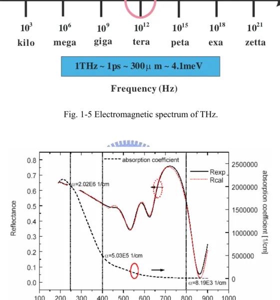
1.4 Time-Resolved Terahertz Spectroscopy
Terahertz (THz= 1012 Hz) has been strongly studied for last two decades. The opening of THz era not only made significant contribution to ultrafast phenomena, but also opened wide applications to optoelectronics and biomedical fields. The THz field is roughly defined by the frequency range of 0.1 to 10 THz (see Fig. 1-5), which corresponds to the wavelength of 0.003 to 3 mm. In 1981, Mourou and Auston firstly demonstrated generation and detection THz radiation by a photoconducting switch [47-48]. It was followed by the study of photoconductor dipole antenna as the THz sensor in 1988 [49]. Afterward plenty of works were focused on the dipole antenna and semiconductor surface electric field for THz generation [50-51]. Free-space electro-optic sampling (FS-EOS) technique was further studied by X. C. Zhang et al. to improve signal to noise ratio and dynamic range [52].
THz has highly potential for many applications. In the bioscience, the photon energy of THz is much smaller than X-ray and therefore will not cause harmful photoionization in biological tissues. THz is also hot for chemical detection, mail or luggage inspection, gas spectroscopy, non-contact and non-destructive measurements. The spectroscopic technique using pulsed THz radiation, terahertz time-domain spectroscopy (THz-TDS), has been developed by taking advantage of short pulses of broadband THz emission. THz-TDS has a
time resolution of sub-picosecond and corresponds to a spectral resolution of 50 GHz. Since THz-TDS is a non-destructive measurement, it is suitable for the study of dielectric materials and semiconductors. For example, Grischkowsky et al. use THz-TDS for the study of carrier concentration and absorption characteristics of sapphire and silicon in THz frequency. Therefore we will also use THz-TDS for the non-destructive measurement of poly-Si annealed by Ti:Sapphire laser.
1.5 Motivation
Hydrogenated amorphous silicon (a-Si:H) is used extensively in Thin Film Transistors (TFTs) for Flat Panel Displays (FPDs) and large area imagers, and it is also a promising photovoltaic material. The a-Si:H TFTs have low off-current and sufficient on-current for most applications. However, a-Si:H shows poor carrier mobility due to its disordered crystal structure. The poor mobility will result in the limitation on the pixel sizes for display and other imaging applications. Therefore, poly-Si with higher mobility up to 300cm2/Vs has been suggested as an alternative of a-Si:H. Recently, high performance poly-Si devices have been applied in many applications such as flat panel displays.
Poly-Si can be obtained by furnace annealing and ELA applied on a-Si. However, the process temperature of furnace annealing is 550 °C, which may induce the melting of glass substrate. Considering of the long pulse duration (~10 ns) of excimer laser, the melting process of a-Si layer is still thermal melting, which starts via the lattice vibration. Therefore, we try to induce nonthermal melting by irradiate the a-Si layer with ultrafast laser pulses (~50 fs) for comparison. The laser pulse promotes electrons from valance (bonding) states to conduction states, resulting in destabilization of the bands and softening of phonon modes. The semiconductor may lose its lattice structure when the phonon modes soften to certain point and undergo a phase transition [13-15]. The effect was observed in semiconductors under intense femtosecond laser excitation in a time scale of subpicosecond.
This subpicosecond time scale is too fast for carrier to transfer energy to lattice, ruling out the possibility of lattice heating via phonon emission. Therefore, the melting in subpicosecond time scale is named as nonthermal melting. Besides, the linear absorption coefficient of silicon at 250 nm (ELA) is 200 times higher than that at 800 nm (FLA) as shown in Fig. 1-6. The nonlinear absorption may play an important role in FLA. After the laser crystallization process, it is also important to put the poly-Si on TFT fabrication. Thus we can analyze the electrical characteristics and the defect state density of femtosecond laser annealed (FLA) TFT.
Dopant profile engineering is potentially a promising approach for the formation of thin insulators, short channels, and shallow junctions for scaling of transistor-based silicon devices to ~100 nm. Activation by ELA has been shown to outperform FA and even RTP (or RTA) on minimizing dopant diffusion. However, dopant diffusion during ELA-based activation is still observed by photoexcited lattice systems like thermally heated lattice systems. Therefore, FLA seems to have a high potential to reduce the lattice heating by reducing the activation duration with ultrashort laser pulses. After activation process, we can analyze the dopant profile and sheet resistance of FLA-processed sample to ensure the activation efficiency.
Since the grain size of poly-Si is one of the key features to affect electrical characteristics of TFTs such as mobility, it is important to examine the grain size of poly-Si before TFT-fabrication. Traditionally, the grain size is examined by scanning electron microscopy (SEM). However, a destructive sample preparation, such as Secco etching is required for SEM. The Secco etch, using (HF + K2Cr2O7 + H2O in a ratio of HF : H2O = 2 :
1 with 44 g K2Cr2O7 dissolved in 1 L of the H2O has been frequently used to delineate the
grain boundary of poly-Si. Besides, SEM picture is limited with a tiny observation area, which can not offer the information about the grain quality in a large area. In this study, the carrier mobility of FLA poly-Si is measured by optical-pump–THz-probe (OPTP) technique.
We also measured the temporal evolution of far-infrared conductivity and refractive index of FLA poly-Si. This technique is contact-free, therefore, damage-free. The quality of poly-Si samples annealed at various pump fluence can be directly identified by OPTP technique.
1.6 Organization of thesis
In Chap. 2, the grain size of FLA-processed poly-Si is firstly analyzed in order to obtain the annealing parameter of FLA. The characteristics of FLA-processed poly-Si are also analyzed by various techniques. The electrical characteristics of FLA-processed TFTs are also measured and applied for the calculation of defect state density.
In Chap. 3, the results of dopant profile engineering by FLA will be shown. The activation parameter which is affected by various sample preparation parameters will also be shown. We will discuss the mechanisms of dopant diffusion due to ion implantation with different ions and different activation parameters. Our results show that FLA has a high potential for future application on ultra-shallow junction activation. Not only the ultra-shallow formation in silicon substrate is important, bulk germanium (Ge) gains the attention for its significantly high carrier mobility. Our preliminary results will be shown in this chapter.
The results of FLA-processed poly-Si analyzed by THz-TDS will be shown in chapter 4. Poly-Si in two different grain sizes can be easily distinguished by OPTP technique. The mobility can also be obtained by fitting the results of THz-TDS measurements with the Drude model. The reason that the increase of mobility for large grain size poly-Si measured by OPTP will be discussed.
References
[1] K. Sera, F. okumura, H. Uchida, S. Itoh, S. Kaneko and K. Hotta, “High-performance TFTs fabricated by XeCl excimer laser annealing of hydrogenated amorphous-silicon film,” IEEE Trans. Electron Devices, vol. 36, pp. 2868-2872, 1989.
[2] J. G. Blake, J. D. Stevens, and R. Young, “Impact of low temperature polysilicon on the AMLCD market,” Solid State Tech., vol. 41, pp. 56-62, 1998.
[3] S. Sriraman, S. Agarwal, E. S. Aydil, and D. Maroudas, “Mechanism of hydrogen-induced crystallization of amorphous silicon,” Nature, vol. 418, pp. 62-65, 2002.
[4] G. A. Bhat, Z. Jin, H. S. Kwok, and M. Wong, “Effects of Longitudinal Grain Boundaries on the Performance of MILC-TFT’s,” IEEE Electron Device Lett. vol. 20, pp. 97-99, 1999.
[5] J. S. Im, H. J. Kim, and M. O. Thompson, “Phase transformation mechanisms involved in excimer laser crystallization of amorphous silicon films,” Appl. Phys. Lett., vol. 63, pp. 1969-1971, 1993.
[6] G. K. Giust, and T. W. Sigmon, “Microstructural characterization of solid-phase crystallized amorphous silicon films recrystallized using an excimer laser,” Appl. Phys. Lett., vol. 70, pp. 767-769, 1997.
[7] S. D. Brotherton, D. J. McCulloch, J. P. Gowers, J. R. Ayres, and M. J. Trainor, “Influence of melt depth in laser crystallized poly-Si thin film transistors,” J. Appl. Phys., vol. 82, pp. 4086-4094, 1997.
[8] J. S. Im, M.A. Crowder, R. S. Sposili, J. P. Leonard, H. J. Kim, J. H. Yoon, V. V. Gupta, H. J. Song, and H. S.Cho, “Controlled Super-Lateral Growth of Si Films for Microstructural Manipulation and Optimization,” Phys. Stat. Sol. A. vol. 166, pp. 603-617, 1998.
and crystal engineering,” Applied Surface Science, vol. 208, pp. 250-262, 2003. [10] M. A. Crowder, P. G. Carey, P. M. Smith, R. S. Sposili, H. S. Cho, and J. S. Im,
“Low-Temperature Single-Crystal Si TFT’s Fabricated on Si Films Processed via Sequential Lateral Solidification ,” IEEE Electron Device Lett., vol. 19, pp. 306-308, 1998.
[11] R. Dassow, J. R. Köhler, Melanie Nerding, M. Grouvogl, R. B. Bergmann, and J. H. Werner, “Laser-crystallized polycrystalline silicon on glass for photovoltaic applications,” Solid State Phen. vol. 67-68, 193-198, 1999.
[12] A. Hara, F. Takeuchi, and N. Sasaki, “Selective single-crystalline-silicon growth at the pre-defined active regions of TFTs on a glass by a scanning CW laser irradiation,” IEEE Electron Devices Society, Proc. of International Electron Device Meeting, pp. 209-212, 2000.
[13] S. K. Sundaram, and E. Mazur, “Inducing and probing non-thermal transitions in semiconductors using femtosecond laser pulses,” Nature Materials, vol. 1, pp. 217-224, 2002.
[14] A. Rousse, C. Rischel, S. Fourmaux, I. Uschmann, S. Sebban, G. Grillon, Ph. Balcou, E. Förster, J. P. Geindre, P. Audebert, J. C. Gauthier, and D. Hulin, “Non-thermal melting in semiconductors measured at femtosecond resolution,” Nature, vol. 410, pp. 65-68, 2001.
[15] K. Sokolowski-Tinten, J. Biakowski, and D. von der Linde, “Ultrafast laser-induced order-disorder transitions in semiconductors,” Phys. Rev. B, vol. 51, pp. 14186-14198, 1995.
[16] T. Y. Choi, and C. P. Grigoropoulos, “Plasma and ablation dynamics in ultrafast laser processing of crystalline Silicon,” J. Appl. Phys., vol. 92, pp. 4918-4925, 2002.
[17] X. Liu, D. Du, and G. Mourou, “Laser Ablation and Micromachining with Ultrashort Laser Pulses,” IEEE Journal of Quantum Electronics, vol. 33, pp. 1706-1716, 1997.
[18] T. Q. Jia, Z. Z. Xu, X. X. Li, R. X. Li, B. Shuai, and F. L. Zhao, “Microscopic mechanisms of ablation and micromachining of dielectrics by using femtosecond lasers,” Appl. Phys. Lett., vol. 82, pp. 4382-4384, 2003.
[19] W. G. Hawkins, “Polycrystalline-silicon device technology for large-area electronics,” IEEE Trans. Electron Devices, vol. 33, pp. 477-481, 1986.
[20] M. Takabatake, J. Ohwada, Y. A. Ono, K. Ono, A. Mimura and N. Konishi, “CMOS circuits for peripheral circuit integrated poly-Si TFT LCD fabricated at low temperature below 600 °C,” IEEE, Trans. Electron Devices, vol. 38, pp. 1303-1309, 1991.
[21] N. Yamauchi and R. Reif, “ Polycrystalline silicon thin films processed with silicon ion implantation and subsequent solid-phase crystallization : Theory, experiments and thin-film transistor applications,” J. Appl. Phys., vol. 75, pp. 3235-3257, 1994.
[22] M. K. Hatalis and D. W. Greve, “Large grain polycrystalline silicon by low-temperature annealing of low-pressure chemical vapor deposited amorphous silicon films,” J. Appl. Phys., vol. 63, pp. 2260-2266, 1988.
[23] E. I. Shtyrkov, I. B. Khaibullin, M. M. Zaripov, M. F. Galyatudinoov and R. M. Bayasitov, Sov. Phys., vol. 9, pp. 1309, 1975.
[24] R. S. Sussmann, A. J. Harris and R. Ogden, J. Nanocrystalline. Solid. vol. 35-36, pp. 249, 1980.
[25] T. Sameshima and S. Usui, Mat. Res. Soc. Symp. Proc., vol. 71, pp. 435, 1986. [26] W. Sinke, F. W. Saris, Phys. Rev. Lett., vol. 53, pp. 2121, 1984.
[27] J. S. Im, H. J. Kim, M. O. Thompson, Appl. Phys. Lett., vol. 63, pp 2969 1993. [28] J. S. Im and H. J. Kim, Appl. Phys. Lett., vol. 64, pp. 2303, 1994.
[29] A. T. Voutsas, Applied Surface Science, vol. 208, pp. 250, 2003.
[30] T. Sameshima, S. Usui and M. Sekiya, IEEE Electron Device Lett., vol 7, pp. 276, 1986.
[31] H. Kuriyama, Jpn. J. Appl. Phys., Part 1, vol. 30, pp. 3700, 1991. [32] S. M. Sze, Semiconductor Devices physics and Technology.
[33] A. Agarwal, H. J. Gossmann, D. J.Eaglesham, S. B.Herner, A. T. Fiory, and T. E. Haynes, Appl. Phys. Lett., vol. 74, pp. 2435, 1999.
[34] L. S. Robertson, M. E. Law, K. S. Jones, L. M. Rubin, J. Jackson, P. Chi and D. S. Simons, Appl. Phys. Lett., vol. 75, pp. 3844, 1999.
[35] A. Agarwal, H. J. Gossmann, D. J.Eaglesham, L. Pelaz, D. C. Jacobson, T. E. Haynes and Y. Erokhin, Appl. Phys. Lett., vol. 71, pp. 3141 1997.
[36] R. Duffy, V. C. Venezia, A. Heringa, T. W. T. Husken, M. J. P. Hopstaken, N. E. B. Cowern, P. B. Griffin, and C. C. Wang, Appl. Phys. Lett., vol. 82, pp. 3647, 2003. [37] Y. F. Chong, K. L. Pey, A.T. S. Wee, A. See, L. Chan, Y. F. Lu, W. D. Song and L. H.
Chua, Appl. Phys. Lett., vol. 76, pp. 3197, 2000.
[38] C. H. Poon, B. J. Cho, Y. F. Lu, M. Bhat and Alex See, J. Vac. Sci. B, vol. 21(2), pp. 706, 2003.
[39] C. H. Poon, L. S. Tan, B. J. Cho, Alex See and M. Bhat, Journal of The Electrochamical Society, vol. 151(1), pp. G80, 2004.
[40] H. C. H. Wang, C. C. Wang, C. S. Chang, T. Wang, P. B. Griffin,and C. H. Diaz, IEEE Electron Device Lett., vol. 22, pp. 65, 2001.
[41] A. Agarwal, D. J. Eaglesham, H.-J. Gossmann, L. Pelaz, S. B. Herner, D. C. Jacobson, T. E. Haynes, Y. Erokhin, and R. Simonton, Tech. Dig. Int. Electron Devices Meet., pp. 467, 1997.
[42] S. T. Dunham, S. Chakravarthi, and A. H. Gencer, Tech. Dig. Int. Electron Devices Meet., pp. 501, 1998.
[43] V. Privitera, C. Spinella, G. Fortunato and L. Mariucci, Appl. Phys. Lett., vol. 77, pp. 552, 2000.
van der Heide and W. K. Chu, J.Appl. Phys., vol. 92, pp. 5788, 2002. [45] S. Baek, T. Jang and H. Hwang, Appl. Phys. Lett., vol. 80, pp. 2272, 2002.
[46] S. Whelan, A. L. Magna, V. Privitera, G. Mannino, M. Italia,C. Bongiorno, G. Fortunato and L. Mariucci, Phys. Rev. B, vol. 67, pp. 075201, 2003.
[47] Mourou G, Stancampiano C V, Antonetti A and Orszag A, “Picosecond microwave pulse generation,” Appl. Phys. Lett., vol. 38, no. 6, pp. 470, 1981.
[48] Auston D H, Cheung K P and Smith P R, “Picosecond photoconducting Hertzian dipoles,” Appl. Phys. Lett., vol. 45, no. 3, pp. 284, 1984.
[49] Ch. Fattinger, and D. Grischkowsky, “Point source terahertz optics,” Appl. Phys. Lett., vol. 53, pp. 1480, 1988.
[50] N. Sarukura, H. Othtake, S. Izumida, and Z. Liu, “High average-power THz radiation from femtosecond laser-irradiated InAs in a magnetic field and its elliptical polarization characteristics,” J. Appl. Phys., vol. 84, pp. 654, 1998.
[51] X.-C. Zhang, Perspectives in Optoelectronics, Ed. By Sudhanshu S. Jha, Would Scientific, chapter 3, 1995.
[52] Q. Wu and X. C. Zhang, “Ultrafast electro-optic field sensors,” Appl. Phys. Lett., vol. 68, no. 12, pp. 1604, 1996.
Figures
Fig. 1-1 Grain size and corresponding poly-Si TFT mobility vs. laser fluence for conventional ELA process [29].
Fig. 1-2 SLG growth initiates from the seeds, which survived in the melting process, at the Si-SiO2 interface [29].
Fig. 1-3 SIMS profiles of a 20 keV BF2 2×10¹⁵/cm2 before and after annealing. The
annealing process was performed by RTA or ELA [43].
Fig. 1-4 Comparison of boron concentration profiles after laser annealing with successive pulses at 1 J/cm2.
103 106 109 1012 1015 1018 1021
kilo mega giga tera peta exa zetta
Visible x-ray Microwaves Photonics Electronics γ -ray Thz Frequency (Hz) 1THz ~ 1ps ~ 300μ m ~ 4.1meV
Fig. 1-5 Electromagnetic spectrum of THz.
Chapter 2
Femtosecond Laser Crystallization of Amorphous Silicon
Thin Films and Characterizations of Crystallized
Polycrystalline Silicon Thin Film Transistors
2.1 Introduction
With the demand of larger display area and pixel density of thin film transistor liquid crystal display (TFT-LCD), high mobility TFTs are required for pixel driver of TFT-LCD in order to shorten the charging time of pixel electrodes. Low temperature poly silicon (LTPS) technology has been studied for the purpose integration of drivers at the periphery of active matrix liquid crystal display [1]. Because of its better crystalline quality than amorphous silicon (a-Si), especially the grain size, poly-Si attracted a great attention for last two decades [2-5].
Unlike annealing and activation using continuous-wave (CW) and long pulse lasers, nonlinear photo-energy absorption and non-equilibrium thermodynamics are expected to dominate the interactions between the intense femtosecond laser pulses and irradiated transparent materials [6-11]. Such a non-linear process provides precise and low-threshold fluence associated with femtosecond laser-ablation [8-11]. Due to non-linear photon absorption, the melting of crystal silicon takes place in very short time scale, after 100-800 fs depending on fluence [8]. The purpose of this work is to develop a new approach of using ultrafast laser for recrystallization of a-Si. The quality of poly-Si will be analyzed by SEM and AFM et al. and further examined by measuring the electrical characteristics of FLA-processed TFTs. Good transistor characteristics, as confirmed by measurements of
electrical parameters and grain trap-state densities were obtained for a wide process window of annealing laser fluences.
Firstly, general features of femtosecond laser will be discussed in this chapter. Secondly, the experimental setup of laser annealing will be shown. This will be followed by sample preparation of a-Si and TFT processing for poly-Si. The analyzing results of poly-Si annealed by FLA by several different instruments will be shown in Sec. 2.4.1. The electrical characteristics of FLA-processed TFTs will be shown in Sec. 2.4.2.
2.2 General Features of Femtosecond Lasers
The invention of the laser in 1960 stimulated the development of optical physics and gave rise to many rising research fields. One of these rising research fields was ultrafast optics, which was raised and developed in mid-1960s with the production of nanosecond (10-9 s) pulses by the first mode-locked laser. Nowadays, a lot of progresses of ultrafast optics lead to some practical lasers which can produce pulses in the femtosecond (10-15 s) time scale. Early in the 1990s, Ti:Sapphire femtosecond lasers became commercially available and ultrafast optoelectronics began to spread all over the world. In this section, our femtosecond laser system will be briefly introduced.
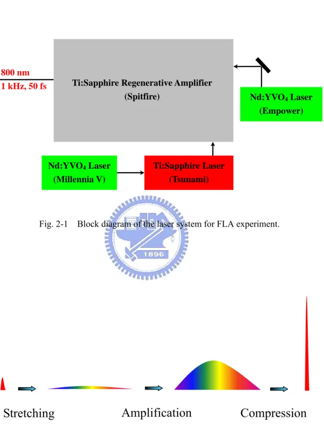
Our femtosecond later system is shown as the block diagram in Fig. 2-1. We use the Ti:Sapphire laser as the seeding laser which is then injected into the Ti:Sapphire regenerative amplifier (Spitfire, Spectra-Physics) for amplification.
The pump laser for the Ti:Sapphire laser (Spectra Physics Tsunami) is a 5W frequency doubled diode-pumped Nd:YVO4 laser (Millennia Vs, Spectra-Physics) with a wavelength
λ=532 nm. The Ti:Sapphire laser provides an output train of intense 35 fs pulses with wavelengths ranging from 770nm to 830 nm. The pulse repetition rate is ~82 MHz and the output power can reach 0.5 W.
The pump laser for the amplification process in Spitfire is a Q-switched Nd:YVO4
laser. This Nd:YVO4 laser delivers a high average power output of 20 W at 527 nm. The
chirped-pulse amplification diagram of Spitfire is shown in Fig. 2-2. The Spitfire amplifies the seeding pulses by a million times from pulse energy of 6 nJ to 2 mJ. The repetition rate is 1 kHz and the output average power is 2 W. The properties of the Ti:Sapphire regenerative amplifier are shown in Table 2-1.
2.3 Experiment setup and procedures
2.3.1 The Setup of Femtosecond Laser Crystallization and Sample
Preparation
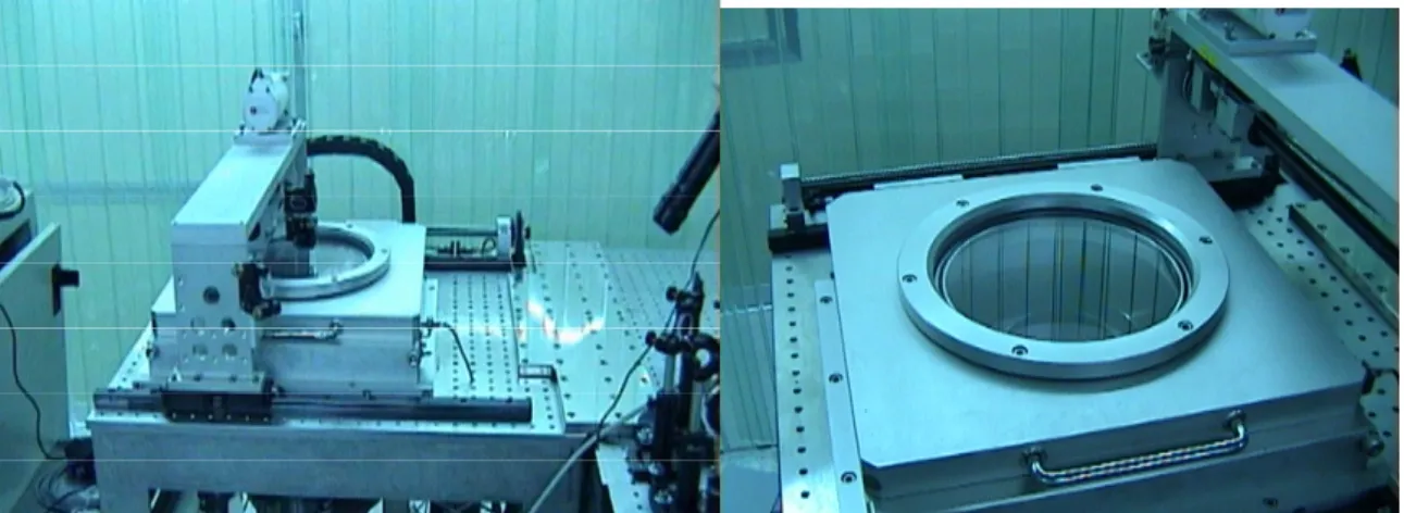
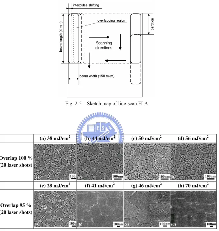
Silane-based a-Si films (100 nm) were deposited on oxidized (500 nm) silicon wafers by low-pressure chemical vapor deposition (LPCVD) at 550 °C. An infrared femtosecond Ti:Sapphire laser system (TSUNAMI, and SPIT FIRE, from Spectra-Physics company) with a wavelength of 800 nm, a repetition rate of 1 kHz, a pulse duration in the range of 50-125 fs, and an output energy per pulse of ~0.5 mJ, was guided to crystallize amorphous silicon as shown in Fig. 2-3. All samples were placed in a vacuum chamber, and a heater increased the substrate temperature up to 400 °C (see Fig. 2-4). A two-axis transition stage was used for the line-scan FLA as shown in Fig. 2-5.
First, we made a steady-state multiple shots FLA experiment (overlapping 100% with 20 laser shots). The pulse train from the mentioned laser system was focused in the strip spot (3 mm×250 μm). We changed the fluence (38-63 mJ/cm2) and the number of shots (5-100). For comparison, we also processed the line-scan FLA with different laser fluence (28-70 mJ/cm2) and interpulse overlapping (10-99%), which corresponds to the number of laser shots from 10-99.
2.3.2 Fabrication of Femtosecond Laser Crystallized Poly-Si TFTs
Amorphous Si layers of 100 nm were deposited by low pressure chemical vapor deposition (LPCVD) at 550 °C on 500 nm-SiO2-coated silicon wafers. The active layers for
the TFTs were crystallized by line-scanning irradiation of twenty ultrafast (~ 50 fs) near-infrared (λ = 800 nm) laser pulses with fluences of 34-50 mJ/cm2 (or total fluences of
20 laser pulses about 0.68-1.0 J/cm2). The beam spot size was 8 mm ×110 μm. During the scanning process, the overlapping of neighboring pulses was fixed at 95%. FLA was conducted on a substrate heated at 400 °C in a vacuum chamber. FLA-crystallized layers were then defined into active regions for transistors with channel length (L)/ channel width (W) of 2μm/2μm, 3μm/3μm, 5μm/5μm, and 10μm/10μm. A SiO2 gate dielectric layer of 50
nm and polycrystalline silicon gate layer of 150 nm were then grown by LPCVD and patterned for self-aligned phosphorous implantation with dosage of 5×1015 cm-2, and energy of 53 keV. After thermal activation and metal connection were performed, n-type transistors were completed.
For comparison, TFTs with channels crystallized by furnace annealing (solid phase crystallization, SPC) in nitrogen ambient at 600 °C for 24 hours were also processed on the same run. The transfer characteristics (drain current Id versus gate voltage Vg) of the devices
were measured at a drain voltage Vd = 0.1 V, to extract electrical parameters. Grain
trap-state densities, nGT, for all TFTs were also examined using the field-effect conductance
method [12].
2.4 Results and Discussions
2.4.1 Material Characterization of Femtosecond Laser Crystallized
Poly-Si Thin Films
uniformity of poly-Si grains. Pictures from (a) to (d) in Fig. 2-6 represent steady-state multi-shot samples irradiated with 20 laser pulses of 50 fs with different energy densities. The average grain size is relatively small (smaller than 50 nm) and almost independent on the energy density. It should be mentioned that in comparison to linear ELA for non-linear steady-state FLA, small grains (<50 nm) might probably be due to the fact that fast cooling (or laser-energy turn-off) associated with short pulses causes random recrystallization from more nucleation sites [5].
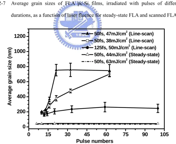
The situation is dramatically changed when we introduce scanning. In our second experiment we scan the laser beam along the sample with the speed of 2.5-25 mm/sec (10-100 laser-shots per unit area, or, equivalently, an overlapping of 90-99%). Pictures from (e) to (h) in Fig.2-6 represent line-scan FLA samples irradiated with 95% interpulse overlapping of 50 fs laser pulses with different energy densities. As shown in Fig. 2-7, the average grain sizes of FLA pc-Si films are plotted as a function of laser energy density (denoted as EL) and pulse duration for both steady-state and line-scan FLA. Herein,
annealing parameters for line-scan (steady-state) FLA were overlapping ~95 % (20 laser-shots).
For line-scan FLA using 125 fs pulses, the grain sizes of the crystallized a-Si films initially increased, and then saturates, before finally declining as the laser fluence was increased from 35 mJ/cm2 to 61 mJ/cm2. The maximum average grain size was around 200 nm when a-Si films were irradiated at 50 mJ/cm2. Despite the difference between the mechanism of photoexcitation-melting using FLA (non-linear annealing) [6-10] and that using nanosecond or longer pulse laser annealing (linear annealing), such as ELA, lateral elongating still dominates the growth of grains in FLA pc-Si films.
With reference to SLG phenomena [5, 13-14], laser fluence (grain sizes) in line-scan FLA can be reasonably divided into three major regimes of partial-melting (small grains), near-complete-melting (largest grains), and complete-melting (fine grains), which fit well
the trends plotted in Fig. 2-7. For line-scan FLA using short pulses with 50 fs duration, the trend in average grain sizes of FLA pc-Si films versus EL is similar to that obtained with
125 fs pulses, but the maximum average grain size (800 nm) of crystallized films, and the optimal EL of crystallization (47 mJ/cm2) for FLA using 50 fs pulses are markly better than
those for FLA using 125 fs pulses. The increase in the efficiency of nonlinear photo-energy absorption [15-16] with the peak power of the laser pulses during infrared FLA, is responsible for the dependence of the grain sizes of line-scan FLA pc-Si films on the duration of pulses, and the laser fluence.
It is remarkable that the maximum of average grain size (~800 nm) equals the wavelength used. This phenomenon is also observed in ELA: in multiple pulse irradiations [15]. Typically, this is related to the interference effects at the surface due to reflection of the hillocks that are formed at the grain boundaries. But in FLA we do not observed such kind of phenomena in the steady-state multiple shots experiment. Only scanning leads to grain elongating. Therefore, we may conclude that we observed the SLS(sequential lateral solidification)-like mechanism (will be discussed later).
The examination of grain sizes of line-scan FLA pc-Si films crystallized at various overlapping, at ELvalues of 47 mJ/cm2 and 38 mJ/cm2 for 50 fs pulses, and 50 mJ/cm2 for 125 fs pulses, is shown in Fig. 2-8. The required laser-shots is lower for FLA using shorter pulses and higher EL. Typically, 10 to 100 laser-shots are required to perform laser linear annealing [5, 13, 17]. But again we should mention that increasing of the pulse numbers or shots in the steady-state FLA does not result in enlarging of crystallized grains (Fig. 2-8). On the other hand, the data in Fig. 2-7 and 2-8 for line-scan FLA clearly demonstrates the high effectiveness of scanning and non-linear photo-absorption in crystallizing amorphous silicon. Assuming a Gaussian shape of the laser beam, for the steady-state mode, each illuminated point is repeatedly shined by the same energy. The first few laser pulses
transform the amorphous material into the poly-phase with large grain distribution. The last pulses (with the same energy) cannot significantly change that distribution.
In the line-scan mode, each illuminated point is also repeatedly shined. But the shined energy for the considered area is not the same from pulse to pulse. It follows a Gaussian sequence. That is possible reason why smaller grains have possibilities in gaining larger energy, therefore, resulting in grain-re-growing into larger grains. Thus, suggested SLS-like mechanism, assisted with the feature of low melting-energy for small grains obtained with the steady-state FLA, significantly enlarges the grain-size of line-scan FLA pc-Si films. Moreover, for ultra-short laser pulses the melting thickness is determined by non-linear absorption skin depth rather than heat penetration length due to thermal conduction [10], and thus more insensitive to laser-fluence in comparison with that for linear annealing. Besides the proposed SLS-like mechanism, this melting-depth thinning mechanism during FLA is also responsible for the significant process window in laser fluence (45-60 mJ/cm2) for line-scan FLA using 50 fs pulses.
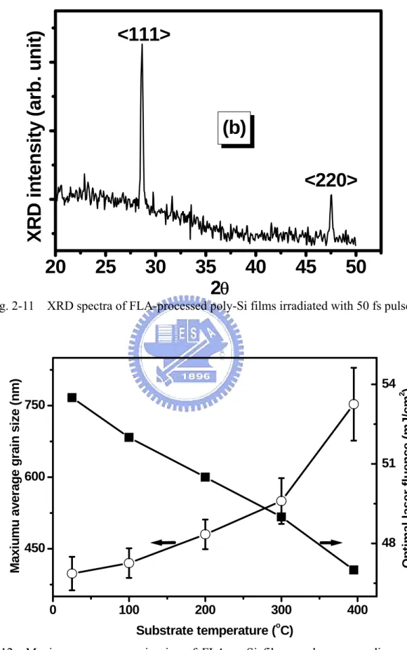
The RMS roughness measured by the atomic force microscopy (AFM) of all FLA pc-Si films is below 4.5 nm. The peak-to-peak roughness is about 26 nm for line-scan FLA samples. Figures 2-9 (b) and (c) represent the AFM images of line-scan and steady-state FLA pc-Si films respectively. The crystalline fraction in such films exceeds 98 %, as calculated from their Raman spectra in Fig. 2-9 (a), in which a sharp peak at 519.5 cm-1, and the absence of a broad peak at 480 cm–1 associated with amorphous phase, implies the high crystallinity of the FLA pc-Si films [16]. Diffraction spots on the TEM selected area diffraction patterns of FLA pc-Si irradiated with 50 fs pulses, presented in Fig. 2-10, reveal that those films are highly crystalline. The corresponding XRD spectrum in Fig. 2-11 shows that the preferred orientation of FLA pc-Si is <111>, same as the orientation of those annealed by other types of lasers [21, 22].
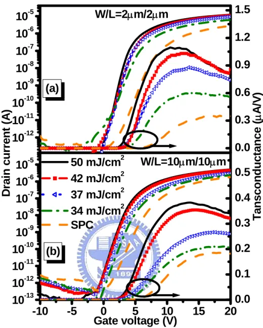
The maximum grain size of FLA pc-Si films increases twice (400 to 800 nm) as the substrate temperature increases from room temperature to 400 °C (see Fig. 2-12). James S. Im et al. observed similar results in ELA pc-Si films, explaining them by a longer time for lateral growth (larger grains) due to higher substrate temperatures (or lower quenching rates [18]). Conventional laser thermal annealing makes the grain sizes of annealed films relatively insensitive to the thermal energy from the substrate temperature, because laser thermal annealing “heats” the lattice to a melting temperature far above the substrate temperature. This implies that the substrate temperature more strongly influences grain growth in films crystallized by FLA using shorter pulses than by ELA using longer pulses, and by laser thermal annealing, thus explaining the trend observed on Fig. 2-12.
2.4.2 Electrical Characterization of TFTs Fabricated by Femtosecond
Laser Crystallization
In Fig. 2-13, we have plotted logarithmic transfer characteristics and linear transconductance (Gm) curves for some representative TFTs fabricated by FLA and SPC.
For TFTs with channel dimensions of W = L = 10 μm and W = L = 2 μm, the on/off current ratio was better than 107. As the laser fluence decreased from 51 to 34 mJ/cm2, significant decrease of Gm was observed due to the deterioration of crystallinity.
The maximum Gm of TFTs fabricated by SPC was lower than that of TFTs annealed by FLA even at the lowest fluence we employed. The maximum values of Gm were analyzed to yield the field-effect electron mobility (μFE). The threshold voltage (Vth) and the
subthreshold slope (S) were then extracted using the procedure described in reference 23. Electrical parameters of FLA-processed TFTs are presented as functions of channel sizes and laser energy in Fig. 2-14.
The Id-Vg curves of TFT with channel dimensions of W = L = 5 μm measured at
Id-Vg curves of TFT with different channel dimensions are not shown here. It is well-known
that the tail-state density of grain traps, NG, closely correlates with channel crystallinity [24]. We find that the values of NG at an energy (E) ~ 0.5 eV above the Fermi level (EF), for
transistors with channels of 5μm/5μm, decrease from ~3.5×10²¹ to 1.5×10²¹eV-1cm-3 as the
laser fluence increases from 37mJ/cm2 to 50mJ/cm2. This is shown in Fig. 2-16. Clearly, larger grains with fewer associated defects were obtained at increasing laser fluence up to 50mJ/cm2. This reduces considerably the height of the barrier to carrier transportation in the channels. As a result, higher Gm values are obtained (see Fig. 2-13). Similar trend for μFE can be observed in Fig. 2-14, regardless of channel sizes.
Increasing channel crystallinity normally reduces the density of the grain defects, including deep-states defects. For example, increasing laser fluences decreases deep-state and midgap-state densities of grain traps for the device with channels of 5μm/5μm, to 4×1018 cm-3 (at E-E
f = ΔE= 0.25 eV), and 1×10¹⁸ eV-1cm-3 (at ΔE~ 0 eV), respectively (See
Fig. 2-16).
Area densities of grain trap-states, NG, at ΔE = 0 eV for devices in Fig. 2-16, are estimated from NG ≈ nGT.tCLC where tCLC represents the thickness of FLA-crystallized polycrystalline silicon. For the same TFT, we find that the values of NG are in good agreement with those of the effective trap state densities Nt calculated from subthreshold slope. Previous workers have shown that the values of NG were more affected by interface defects associated with channel roughness in the ELA processed TFTs [25]. The fact that NG
≈ Nt implies that channel crystallinity rather than channel roughness in such FLA-crystallized polycrystalline silicon layers, which exhibit sub-micro grains and smooth surfaces with roughness of ~ 4-9 nm, dominates electrical characteristics of fabricated transistors (See Figs. 2-14 and 2-16). The deep-state dominated subthreshold slope and threshold voltage both follow the trend of reduction in grain deep-states densities with laser fluence (See also Figs. 2-14 and 2-16) [24]. The grain trap-state densities in Fig. 2-16 also
show that the FLA-annealed TFTs are superior to SPC-annealed TFTs, consistent with that of the electrical parameters presented in Fig. 2-14.
In the range of laser fluences of 37-50 mJ/cm2, the electrical characteristics of TFTs crystallized by FLA vary by at most 30%, regardless of channel sizes. The relatively small variations of electrical parameters for fractional change of fluence (∆E/E) in FLA is lower than that reported (80%) of TFTs fabricated by ELA [26]. Such a wide FLA-crystallization window as determined by transistor characteristics agrees with our studies of structural characteristics of poly-Si crystallized by FLA and grain trap-state densities associated with channel crystallinity as presented herein.
The tail-state densities (at ΔE= 0.5 eV) of FLA-fabricated transistors with different channel sizes were in the range of 6×10²⁰ to 1×10²¹ eV-1cm-3. The values are of the same
order of magnitude as those obtained from ELA-crystallized polycrystalline silicon layers [25]. As a result, mobilities of FLA-fabricated transistors, μFE ≈ 80-160 cm2/Vs, are also comparable to those for ELA-fabricated transistors. We also note that grain trap-state densities for those channels with different sizes but the same crystallinity decline as channel size decreases. Fewer numbers of grain defects in smaller channels will surely result in better electrical characteristics in TFTs as seen in results for FLA-fabricated TFTs (Fig. 2-14) [27].
2.5 Summary
The characteristics and annealing parameters for silicon films crystallized by FLA herein are compared with those obtained by other annealing methods [13, 17-20] and summarized in Table 2-2. The intense ultrashort laser pulses lead to efficient non-linear photo-energy absorption and the generation of dense photoexcited plasma in irradiated materials, enabling melting of a-Si films that are nearly transparent at 800 nm. FLA assisted by spatial scanning of laser strip spot efficiently crystallizes a-Si films with large average
grains of 800 nm, using laser fluence as low as ~45 mJ/cm2, and low number of laser shots (20 shots). Moreover, FLA exhibits a significantly wide operating window for laser-fluence (45-60 mJ/cm2, or, equivalently, ~30% variations), which makes it possible to implement suggested method in the TFT industry.
Polycrystalline silicon transistors fabricated by near-infrared femtosecond laser annealing were demonstrated for the first time. The FLA-annealed poly-Si channels exhibit low tail-state, deep-state, and midgap-state densities of grain traps of ~1×10²¹, ~5×10¹⁸, and
~9×10¹⁷ eV-1cm-3. Field-effect mobility, threshold voltage, and subthreshold slope for
transistors fabricated on poly-Si annealed with a total fluence of 0.9 J/cm2 in a line-scan mode were measured to be 80-160 cm2/Vs, 1-3 V, and 0.4-0.8 V/dec, respectively. A wide process window for annealing laser fluences, 37-50 mJ/cm2, was confirmed by examining the changes in electrical parameters for transistors with various channel dimensions. Thus the performance of FLA-fabricated transistors is comparable to that of ELA-fabricated transistors.
![Fig. 1-1 Grain size and corresponding poly-Si TFT mobility vs. laser fluence for conventional ELA process [29]](https://thumb-ap.123doks.com/thumbv2/9libinfo/8759723.207902/31.892.153.799.145.430/fig-grain-corresponding-mobility-laser-fluence-conventional-process.webp)
![Fig. 1-3 SIMS profiles of a 20 keV BF 2 2×10 15 /cm 2 before and after annealing. The annealing process was performed by RTA or ELA [43]](https://thumb-ap.123doks.com/thumbv2/9libinfo/8759723.207902/32.892.205.730.116.486/fig-sims-profiles-annealing-annealing-process-performed-rta.webp)