運用具有變化關聯性之FR向量以分析訊號變化活動
70
0
0
全文
(2) Switching activity analysis with FR-vector considering transition correlation. 研 究 生:夏文忠. Student:Wen-Chung Shia. 指導教授:陳昌居. Advisor:Chang-Jiu Chen. 國 立 交 通 大 學 資 訊 工 程 學 系 碩 士 論 文. A Thesis Submitted to Department of Computer Science and Information Engineering College of Electrical Engineering and Computer Science National Chiao Tung University in partial Fulfillment of the Requirements for the Degree of Master in Computer Science and Information Engineering June 2004. Hsinchu, Taiwan, Republic of China. II.
(3) 中華民國九十三年六月. 授權書 (博碩士論文) 本授權書所授權之論文為本人在__國立交通__大學(學院)_資訊工程_系所 _______組_九十三_學年度第_二_學期取得_碩士_士學位之論文。 論文名稱:__運用具有變化關聯性之 FR 向量以分析訊號變化活動___ 1.□同意 □不同意 本人具有著作財產權之論文全文資料,授予行政院國家科學委員會科學技術資料中 心、國家圖書館及本人畢業學校圖書館,得不限地域、時間與次數以微縮、光碟或數 位化等各種方式重製後散布發行或上載網路。 本論文為本人向經濟部智慧財產局申請專利的附件之一,請將全文資料延後兩年後再 公開。(請註明文號: ) 2.□同意 □不同意 本人具有著作財產權之論文全文資料,授予教育部指定送繳之圖書館及本人畢業學校 圖書館,為學術研究之目的以各種方法重製,或為上述目的再授權他人以各種方法重 製,不限地域與時間,惟每人以一份為限。 上述授權內容均無須訂立讓與及授權契約書。依本授權之發行權為非專屬性發行權利。依本 授權所為之收錄、重製、發行及學術研發利用均為無償。上述同意與不同意之欄位若未鉤選, 本人同意視同授權。 指導教授姓名:. 陳昌居. 研究生簽名: (親筆正楷) 日期:民國. 學號:9117567 (務必填寫) 九十三年. 六月. 三十日. 1. 本授權書請以黑筆撰寫並影印裝訂於書名頁之次頁。 2. 授權第一項者,所繳的論文本將由註冊組彙總寄交國科會科學技術資料中心。 3. 本授權書已於民國 85 年 4 月 10 日送請內政部著作權委員會(現為經濟部智慧財產局) 修正定稿。 4. 本案依據教育部國家圖書館 85.4.19 台(85)圖編字第 712 號函辦理。. III.
(4) 運用具有變化關聯性之 FR 向量以分析訊號變化活動 研究生:夏文忠. 指導教授:陳昌居 國立交通大學 資訊工程學系 摘要. 為達到低耗能電路設計之目的,估算在閘層時的能量消耗是主要的關鍵之 一。在互補金屬氧化物導體之組合電路中,估算能量消耗可以藉由量測訊號變換 的次數來達成。在本論文中,我們提出結合 FR-Vector 和“布林逼近法"的新 方法。這個方法使用機率的觀念,以時間分割加入時間關聯性的考量,甚至更進 一步用泰勒展開式的逼近法以處理電路間的空間關聯性,然後用少量的資料就可 以模擬出危障、延遲以及重聚合電路的影響。我們將我們的方法、FR-Vector 及 Cadence NC-VHD 對十八個 MCNC 的標竿電路做模擬,並比較所得的結果。得到的 結果顯示我們的方法遠比原 FR-Vector 減低了每一個邏輯閘上的平均加權誤差 值,可從 6.09 個百分點降到 2.77 個百分點。同時,更大幅降低了誤差的尖峰值 -由 23.74 個百分點降到 13.24 個百分點。最後,我們的方法不僅改進了原使用 FR-Vector 時會產生的誤差,執行時間也幾乎與原 FR-Vector 相近。比起使用 NC-VHDL 模擬電路所花費的時間,差距更可到達三十多倍。實際上,相對於對我 們的方法而言,因為電路大小對 NC-VHDL 的影響更為明顯,所以在實際的電路 中,增加的速度更將不止於三十倍(實際電路通常會比我們所測的標竿電路為 大)。. I.
(5) Switching activity analysis with FR-vector considering transition correlation. Student : Wen-Chung Shia Advisor : Dr. Chang-Jiu Chen Department of Computer Science and Information Engineering National Chiao-Tung University. Abstract In the research of the low-power circuit design, one of the key issues is to estimate the power dissipation in a gate-level implementation. In CMOS combinational circuit, the switching activity measurement is an approach to the power dissipation estimation. In this thesis, we propose a new method to combine the FR-Vector model and the concept of Boolean approximation method. We use probabilistic method that time to divide a clock into several time units, and exploit Taylor expansion, then glitches and reconvergent circuit effect can be handled easily. For performance evaluation, we make comparisons among the proposed method, the FR-Vector, and Cadence NC-VHDL in 18 MCNC benchmark circuits. The comparison results show that our method decreasing the weight error percentage (the error percentage in each gate) very much- from 6.09% to 2.77%. Meanwhile, it by far decreases the peak value of error percentage - from 23.74% to 13.24%. Finally, our method not only improves the error caused by the FR-Vector, but also the time it spends is closed to the FR-Vector. Comparing to the simulation of NC-VHDL in the time spending, out method could speed up to 33 times. Moreover, in real circuits, the speed-up would be more than 33 times. It is because the variable “gate count” affects time complexity in NC-VHDL much than the time complexity in our method, and in real circuits, there is usually a larger gate count than our benchmark.. II.
(6) Acknowledgment 完成這篇論文要感謝的人很多,首先感謝指導老師陳昌居老師在提供穩定的 環境與資源讓我能有所成長,也感謝老師在這兩年給予我的協助。特別感謝黃年 畤學長,在完成這篇論文的期間一起討論以及引導,也感激同實驗室的夥伴們曾 經提供的協助以及生活上的點點滴滴。最重要的是感謝我的家人與親友給我的支 持,讓我能夠穩定的求學以及研究,尤其是父親的苦心栽培。. III.
(7) Contents 摘要 ............................................................................................................................... I. ABSTRACT.................................................................................................................II ACKNOWLEDGMENT ........................................................................................................ III. CHAPTER 1 INTRODUCTION................................................................................1. CHAPTER 2 RELATED WORK...............................................................................5. 2.1 BASIC DEFINITION IN SWITCHING ACTIVITIES ESTIMATION .............................5 2.2 PREVIOUS RESEARCH OF SWITCHING ACTIVITIES ESTIMATION .......................6 2.3 FR-VECTOR .........................................................................................................9 2.3.1 Signal Modeling with FR-vector...........................................................................................9. 2.3.2 FR-Vector Logic Composition ............................................................................................10. 2.3.3 FR-Matrix ........................................................................................................................... 11. 2.3.4 Non-Zero Delay FR-matrix ................................................................................................14. 2.4 BOOLEAN APPROXIMATION METHOD (BAM)..................................................15 2.4.1 Basic Assumptions...............................................................................................................15. 2.4.2 Signal probability ................................................................................................................16. 2.4.3 Algorithm of BAM...............................................................................................................21. 2.4.4 Switching Activities .............................................................................................................21. IV.
(8) 2.4.5 Example...............................................................................................................................22. 2.5 REAL-DELAY BOOLEAN FUNCTION (RDBF) ....................................................24. CHAPTER 3 FR-VECTOR WITH BAM................................................................27. 3.1 REVIEW AND INTEGRATION ...............................................................................27 3.2 BASIC DEFINITION AND ASSUMPTION ................................................................28 3.3 PROBABILITIES PROPAGATION ..........................................................................31 3.3.1 Propagation of the Cofactor Transition Relation...............................................................31. 3.3.2 Propagation of the FR-Matrix............................................................................................34. 3.4 AN EXAMPLE OF FR-VECTOR WITH BAM .......................................................39 3.5 RECONVERGENT CIRCUIT IN LIMIT DEPTH .....................................................41 3.6 NON-ZERO DELAY MODEL................................................................................42 3.7 IMPLEMENTATION ..............................................................................................47. CHAPTER 4 EXPERIMENTAL RESULTS...........................................................51. CHAPTER 5 CONCLUSIONS AND FUTURE WORKS .....................................57. REFERENCE: ...........................................................................................................59. V.
(9) List of Figure Figure 1-1: A simple reconvergent circuit..................................................................4 Figure 2-1: 2-input AND gate with n primary inputs. ............................................17 Figure 2-2: General case in the circuit .....................................................................20 Figure 2-3: A test circuit. ...........................................................................................22 Figure 2-4: A logic circuit with non-zero delay gates..............................................25 Figure 3-1: An example of supply set of the reconvergent circuit. ........................30 Figure 3-2: A reconvergent circuit and the FR-Matrix of its input node x. .........34 Figure 3-3: A reconvergent circuit with non-unit delay gate .................................45 Figure 3-4: The pseudo-code of this paper ..............................................................47. VI.
(10) List of Table Table 1-1: The switching state of a 2-bit counter.......................................................4 Table 2-1: the logic composition tables for basic logic function in FR-vector ... 11 Table 2-2: (a) Signal sampling. (b) Its FR-matrix.................................................12 Table 2-3: An example of FRM composition: Input FRM 1, (b) Input FRM 2, and (c) Output FRM. .........................................................................................13 Table 3-1: The composition table for cofactor transition relation. .....................33 Table 3-2: The transition probabilities of primary inputs of the circuit in example 3.4 .........................................................................................................40 Table 4-1:. Switching activity comparisons between NC-VHDL logic simulator,. FRM model and FR-Vector with BAM based on MCNC benchmark circuits with no glitch input. ...........................................................................................52 Table 4-2: The CPU Time for NC-VHDL simulation...........................................54 Table 4-3: The CPU Time for FR-Vector simulation............................................54 Table 4-4: The CPU Time for FR-Vector with BAM simulation.........................54 Table 4-5: The comparison with FR-Vector and with NC-VHDL. .....................55 Table 4-6: Comparison among different technique. ...............................................56. VII.
(11) Chapter 1 Introduction In circuit design, the decreasing of the feature size leads to the increasing of chip density. While the operating frequency growing rapidly and the feature size getting smaller, these factors make the power consumption to be taken into account seriously. Especially, with the rapid, strong demand development in market sectors such as wireless application, laptop and portable medical devices, it makes the power consumption to be one of the most critical topics in digital system design [1]. Time-to-Market requirement could be achieved by low power design techniques and power estimation methodology. With the aid of power estimation function of CAD tools, it can help designers to meet the power specification earlier in designing phase, and further reduce redesign cost at the same time. Power consumption in a CMOS circuit can be classified into following three categories: 1. Static leakage power; 2. Short-circuit power; 3. Dynamic power. In a well-designed circuit, if we don’t consider the special case such as the power lost when portable device is in a dormant state, the total power dissipation cost by the dynamic power consumption of the nodes, which arises due to the charging and discharging of the parasitic capacitance during switching, will by far exceed the first two factors. In [2], the average power consumption at a gate is given by P ( x) = 0.5Vdd2 f clk Cload sw( x) , where Vdd is the supply voltage, f clk is the clock. frequency, Cload is load capacitance, and sw( x) is the switching activity of the. 1.
(12) output node x [2], so we could know sw( x) is a very important factor in power estimation. In power estimation, both speed and accuracy are the most important factors, but obviously, they conflict with each other. The easiest and most direct method of how to estimating power consumption is to simulate the operation of the whole circuit. However, though this method has the most accurate outcome, it also takes too much time. Today, the techniques of power estimation could be divided into two categories: dynamic (statistic) and static (probabilistic) [1] [2]. Dynamic techniques explicitly simulate the circuit under a “typical” input stream. These techniques provide a high level of accuracy but it also takes a very high run time which is because the required number of simulation vectors is usually large. Static techniques would calculate the input patterns first, and use a probability to represent a signal state, and then it propagates or calculates these probabilities from the primary inputs to the output of the whole circuit. In final, it uses these probabilities to get the number of switching. These techniques could provide fast measurement without losing accuracy too much. Gate delay is an important factor about the accuracy in estimations, but it’s very hard to consider the delays in a circuit. For this reason, many papers tried to ignore the impact caused by gate delays [1] [3] [6][9][10][15]. z. Zero delay models: all the gate delays of the circuit are taken as zero.. z. Non-zero delay model: each gate delay of the circuit is a positive number. or zero. We suppose that non-zero delay model with inertial mode in this paper. The most important drawback to activities analysis when without considering gate delay is glitch ignoring. However, in non-zero delay model, glitches could happen from the difference of arrival time between two (or more) input signals, and these glitches would cause additional 20% power estimation in average. In some 2.
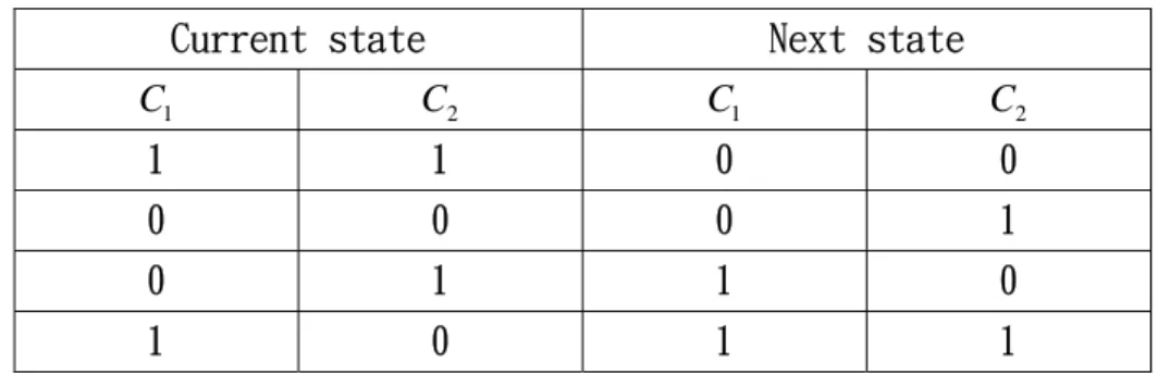
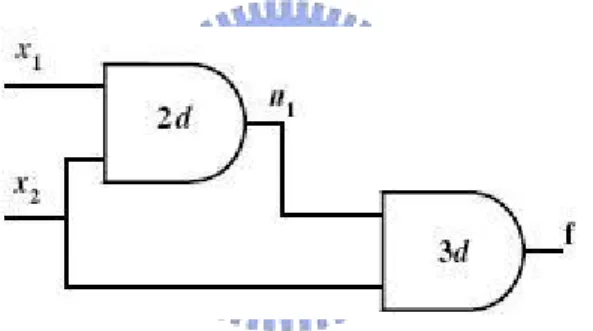
(13) special cases, like specific adder, the additional consuming power could be up to 70% [3]. In additional to glitches, another important factor to power estimation techniques is correlations between signals. There might be two kinds of correlations between signals: temporal dependence and spatial dependence. z. Temporal dependency: Signals may be temporally dependent; in other. words, the next value of a signal may depend on its current or previous values. z. Spatial dependency: Spatial dependency comes from two aspects: 9. Structure dependency is due to reconvergent fanout in the circuit;. 9. Input dependency is that spatial and/or temporal correlations among. the input signals which result from the actual input sequence applied to the target circuit. The input of a counter is an example of dependencies between inputs; Table 1-1 shows the transition of a two-bit counter. In input C2 , the next state is depended on the current state, this is a kind of temporal dependency, and in input C1 , its next state is not just depended on the current state, it would also depend on C2 , this is a kind of spatial dependency. Figure 1-1shows another kind of spatial dependency. In this circuit, the logic. value of node m and n are not dependent due to they are diverge node from node b. m and n convergent at node z for a while. For this reason, we should process the correlation between node m and node n to analyze the switching activities in node z precisely. The aim of this thesis is to propose a modified FR-vector [5]. FR-vector is a model for power consumption which uses probability technique. It could operate under multiple input switching, non-zero gate delay and even glitches happen in a 3.
(14) combinational circuit. We combine the advantages of FR-vector Current state. Next state. C1. C2. C1. C2. 1. 1. 0. 0. 0. 0. 0. 1. 0. 1. 1. 0. 1. 0. 1. 1. Table 1-1: The switching state of a 2-bit counter.. Figure 1-1: A simple reconvergent circuit.. and the Boolean Approximation Method (BAM) [6], which is a data structure to process signal correlation ,then propose a new modified FR-vector - FR-vector with BAM. The rest of this thesis is organized as follows. Chapter 2 introduces some estimation methods and reviews FR-vector and BAM. Chapter 3 describes new modified FR-model. Chapter 4 shows some experimental results. Chapter 5 gives our conclusions and the directions for future development.. 4.
(15) Chapter 2 Related Work Low power circuit is a more and more important research today. As mentioned in the first chapter, the switching activity is a very important factor in power estimation, and we will pay attention to it in the thesis. In this chapter, a picture about some researches of switching activity analysis will be given; we will also introduce some techniques and definitions needed later. Section 2.1. gives some basic definitions. used in switching activity analysis. Then we will give short review of representative researches in section 2.2 . Section 2.3 introduces FR-vector. Section 2.4 describes Boolean approximation Method (BAM). Finally, the Real Delay Boolean Function (RDBF) is introduced in section 2.5 .. 2.1 Basic Definition in Switching Activities Estimation Before discussing the techniques of switching activity estimation, we will introduce some terms or some basic definitions which would be frequently used in this thesis. It is the most basic term in switching activity analysis and all calculations in these techniques is based on the physical signal of circuits. z. Physical signal is an electrical signal that appears in an input line.. Then, we could get signal probability immediately: Definition 2.1 (Signal probability): For any signal line x of the circuit, the probability. of x is logic high is denoted as P( x) , and called signal probability. Though signal probabilities could show the states of circuits, we need to get the information about how signal changes in additional. Thus we use switching probabilities to replace signal probabilities. z. Signal switching (an alternate name is switching activity) is the sequence 5.
(16) of continuous signal states: “ ab ”, where a, b ∈ (0,1) , a and b represent the current and the latter state of continuous states respectively. Definition 2.2 (Switching probability): For any signal line x of the circuit, the. switching probability of x is defined as P[( xt = j ∩ xt −1 = i )] , and is denoted by P( xi → j ) , i, j ∈ (0,1) . As we have mentioned in chapter 1, glitches will cause additional power consumption. Actually, the technique that doesn’t consider glitches is unrealistic in usual. Definition 2.3 (Glitch): The glitch is (an) unexpected transition(s) which occur(s). when the signal switches at the time that is not required. A static hazard exists if a signal remains constant after twice (or more) switches during a clock cycle, so there are static 0 hazards, and static 1 hazard. In opposite side, a dynamic hazard exists if a signal changes is not the same at the start and the end of a clock cycle: there are dynamic 1 hazard (start with logic low and end with logic high) and dynamic 0 hazard (start with logic high and end with logic low).. 2.2 Previous Research of Switching Activities Estimation The simplest and the most intuitive method to estimate the switching activity is logic simulation [7] [8]. Logic simulation is the most accurate method but it is also the slowest one. However, most of the actual combinational circuits are so complicated that it is not practical to simulate them immediately. It has been mentioned by many papers about how to use probability to analyze switching activity. However, their accuracy is not all the same due to the detail about how they implemented. We could classify the key factors which affect the accuracy into if they process the correlation inside the circuit and if they process the glitch. 6.
(17) power. The transitions between circuits are often correlated to each others, for example, the reconvergent circuits will complex the switching activity. Further more, the input patterns might hide some correlation inside itself. In another aspect, if we consider for the gate delay in circuits, there are always some unanticipated transition happens, and cause to additional power consumed. Farid N. Najm [2] has introduced the techniques about switching activity analysis in detail. He notes two statistic methods, and categorizes probabilistic techniques into following five classes: A) Signal probability, B) Probabilistic Simulation CREST, C) Transition Density DENSIM, D) using Binary Decision Diagram BDD, and E) Correlation coefficient. In final, he discussed how to extend from combinational circuits to sequential circuits. We could say that correlation coefficient is the most accurate probabilistic method today. In early years, [4] introduces this concept to take care of the signal correlation between circuit nodes. It uses the correlation coefficient to represent the correlation between the probability two signal probabilities multiplied immediately and. the. probabilities. of. two. signal. are. logic. high. in. real,. that. is:. P ( AB) = P( A) P( B)C A, B , where P ( AB) is the probability of ( A ∩ B ) is true (signal A and signal B both are logic high), and C A, B is correlation coefficient between node A and node B. Hence, we could get C A, B =. P( AB) . This technique will passes this P( A) P( B). coefficient through the whole circuit to calculate signal probabilities under correlated effect.. TCijxy,kl =. Someone. extended. p( xi →k ∩ y j →l ) p ( xi →k ) p( y j →l ). ,. this. concept. to. the. transition. of. signals[1]:. where p( xi →k ∩ y j →l ) is the probability of signal A. changed from i to k and signal B changed from j to l at the same time, and. 7.
(18) TCijxy,kl is transition correlation coefficient between A changed from i to k and. signal B changed from j to l at the same time, this technique also uses OBDD to transmit transition correlation coefficient and switching probability through circuits. To pass correlation coefficient through the whole circuit would cost a lot of time, so “Limited depth” and “Limited nodes” was proposed in [9] [10]. They told that if the reconvergent circuit in a circuit exceeds a constant number of gate levels, the signals between circuits could be taken as independent without considering correlation. Because the larger the gate level is, the weaker the correlation between circuits. We should not sacrifice too much time to a negligible correlation. Another disadvantage of correlation coefficient is when the circuit grows lager and lager; it is unrealistic to build OBDD of the whole circuit. This is because it would consume too much memory. There is another technique called Boolean approximation method (BAM) [6] [11], it uses BAM which is a data structure to process correlation between circuit. BAM could be propagated through circuit by logic characteristic without using OBDD. In this way, BAM could save memory to process larger circuit and make the speed up. BAM uses Taylor expansion to calculate the difference between probability two probabilities multiplied immediately and probabilities in real. Most probabilistic methods could not be very accurate for they do not process glitch. In 1999, G-vector was proposed in [12]. Though this model doesn’t discuss switching activity, it gives a way to process about the generation, transmit and elimination of glitch. FR-vector comes from G-vector. It also uses probability to estimate switching activity, and it further discusses the situation about non-zero delay, multiple-input change. There is another similar method called “tagged probabilistic simulation” [13]. Though FR-vector could process glitches, it ignores signal. 8.
(19) correlations.. 2.3 FR-Vector Though FR-vector does not process signal correlations, it is useful to analyze glitching activity. Most papers which talks about how to process glitches would become very complex for the reason that there would be a lot of complex mathematic equations. FR-vector makes glitch processing become easier by taking the calculation of switching probabilities as the calculation of signal probabilities.. 2.3.1 Signal Modeling with FR-vector There are some basic terms used in FR-vector. z. 0/1 sampling: is the method that samples a physical signal node N times in. a clock cycle. By 0/1 sampling, we can get a sequence of length N consist of 0 and 1, which is a representation of the waveform of the physical signal. z. 0/1 sampled signal is the 0/1 sequence representation of a physical signal.. z. Each internal that we sample one time is called a frame. There is an assumption that the sampling rate is so fast that there is at most one or one glitch in a frame.. z. A frame value of 0/1 sample signal is named state.. And in FR-vector, signal switch is: z. Signal switching (an alternate name is Switching activity) is the sequence “01” or “10” part of a 0/1 sampled signal.. FR-vector keeps the information of glitches before and after the gate in circuits, and simulates the glitch propagation, elimination, and generation very well. It models the switching activities as falling and rising, and marked as “F” and “R” for the signal rising and falling. 9.
(20) Definition 2.4 (FR-vector): An FR-vector is a set of {x | x ∈ [0 |1][0 |1| F | R]N −1} ; 0 is. the non-glitch 0 state, 1 is the non-glitch 1 state, F is the falling signal state, R is the rising signal state, and N is the number of frames in a input vector.. It assumes the first frame is the earliest frame, and it is a non-zero delay model in inertial mode. By these assumptions, there will be at most one switching in a frame (In inertial mode, if a glitch appears shorter than a gate delay, it would be elimination, and in FR-vector, a frame is the smallest gate delay of the circuit.). The rule of obtaining a FR-vector from a 0/1 sampled signal is as follows: Extract FR-vector v from a 0/1 sampled signal S z. Base case: The state of the initial frame in v is equal to the initial state of S .. z. General case: . If the state of Si = the state of Si −1 then vi = Si ;. . If the state of Si = 1 and the state of Si −1 =0, then vi = R ;. . If the state of Si = 0 and the state of Si −1 =1, then vi = F .. The rule of getting a FR-vector from a 0/1-sampled signal mentioned above means that the frame value of FR-vector is represented by the state change from the last frame to current one. Assuming that the initial frame is stable from the final frame in the preceding input vector, than the base case of the rule is obtained.. 2.3.2 FR-Vector Logic Composition FR-vector could be used in logic composition according to the corresponding logic composition table. A logic composition table is a table shows what a FR-vector would be given if two FR-vectors of different inputs propagate through a specific logic gate. Table 2-1 shows the logic composition table in FR-vector.. 10.
(21) Table 2-1: the logic composition tables for basic logic function in FR-vector. The item in these tables is get from the meaning of the corresponding input frame values. For example, the meaning of R and 0 is “01” AND “00”, and it will get 0 at the output, for 0 represents “00”.. 2.3.3 FR-Matrix It is unrealistic to calculate all input pattern in a circuit. For this FR-vector must be transformed into another form, called FR-matrix. Definition 2.5 (FR-matrix): A FR-matrix is a 4 × N matrix. Each column in the matrix. represents a frame with the same index, and the entries in the 4 rows will be used to represent the occurrence probability of 0, 1, R, and F in that frame, respectively.. To obtain an input represented by FR-matrix, first, we should sample the input signal line over multiple clock cycles and obtain an FR-vector for each cycle. Second, counts the number of instances of each distinct FR-vector in the input line. Third, for 11.
(22) each frame, compute the occurrence probabilities of each 0, 1, F and R. Then we get a FR-matrix. There is an example about how to get FR-matrix from input sampling.. Table 2-2:. (a) Signal sampling. (b) Its FR-matrix. Example 2.1 First, we sample the signals that appear in an input line over one. hundred cycles, and obtain 100 corresponding FR-vectors. In Table 2-2(a) suppose we get six distinct FR-vectors with the number of instances of the state for each vector. Then we can determine the corresponding FR-matrix by computing the probability of the state in each frame from this table. In this example, there are 80 instances that the first frame is in 0-state (30 in the first FR-vector, 20 in the second FR-vector, and so on). And the total number of instances is 100, so the occurrence probability of 0-state in the first frame is 0.8. Table 2-2(b) shows the corresponding FR-matrix. Theorem 2.1: The expected number of signal switching activities in a FR-matrix for a. signal line is simplified to the value in the rows of R and F, called the weight of a FR-matrix. When a FR-matrix is obtained from the set of FR-vectors which appeared in a signal line, the weight of the FR-matrix is exactly the average weight of each 12.
(23) FR-vector in the signal line.. From Theorem 2.1, we could know the expected number of signal switching activities from a FR-matrix is considered as the total number of signal switching activities over the total number of FR-vectors. From Table 2-2(a), the average estimated number of signal switching activities from FR-vectors is (0 + 1 + 1 + 0 + 1)*0.3 + (0 + 1 + 0 + 1 + 0)*0.2 + (0 + 0 + 1 + 1 + 1)*0.25 + (0 + 0 + 1 + 1 + 0)*0.1 + (0 + 1 + 1 + 1 + 0)*0.1 + (0 + 0 + 0 + 1 + 0)*0.05 = 2.6, and the weight of the corresponding FR-matrix (Table 2-2(b) ) is 0.5 + 0.35 + 0.15 + 0.55 + 0.1 + 0.4 + 0.55 = 2.6. FR-matrix also could be used in composition according logic composition table. Table 2-3 is an example of two input FRMs and the corresponding outputs FRM of a. OR gate.. Table 2-3:. An example of FRM composition: Input FRM 1, (b) Input FRM 2, and (c) Output FRM. 13.
(24) 2.3.4 Non-Zero Delay FR-matrix FR-matrix can group the frame states according to the evaluation dependencies for a given combinational circuit. And we could get the following Theorem: δ Theorem 2.2 : Let N be the frame size, δ be the logic gate delay. Let FRM out. ( RFM in1 , RFM in 2 ) be the output FRM derived from a logic composition with two input FRMs, FRM in1 and FRM in 2 , for a logic gate with delay δ . Let 0 ( RFM in1 , RFM in 2 ) be the output FRM derived from a logic operation with RFM out. two input FRMs, RFM in1 and RFM in 2 , for a zero delay gate. Then δ 0 RFM out = [ RFM out ]δ ,. where [ RFM ]δ denotes the right-shifted FRM for δ times. In other words, the 0 δ ith ( i ≤ N − δ ) frame in RFM out appears in (i + δ )th frame in RFM out . And the jth. δ 0 frame ( 1 ≤ j ≤ δ ) in RFM out will be filled with the first frame in RFM out .. And an FRM is also a statistical average of the signal states over multiple clock cycles. We also can apply the following theorem only when the multi-cycle operations are allowed. r Theorem 2.3 : Let N be the frame size, r be the gate delay. Let RFM out. ( RFM in1 , RFM in 2 ) be the output FRM from a logic composition of two input FRMs,. RFM in1. and. RFM in 2. for. a. gate. with. delay. r.. Let. 0 ( RFM in1 , RFM in 2 ) be the output FRM from a logic operation with two RFM out. input FRMs, RFM in1 and RFM in 2 , for the same gate with a zero delay. Then. 14.
(25) r 0 RFM out = [ RFM out ]r ,. where [ RFM ] r denotes the rotated FRM for r times. In other words, the ith state 0 r in RFM out appears in (((i + r − 1)% N ) + 1)th state in RFM out .. In this thesis, we will take FR-vector as basic model for its ability to process glitches. In additional, it simplifies the calculation in switching activities. The most obvious disadvantage of FR-vector is that it doesn’t consider correlations between signals in circuits. In next section, we describe a technique that takes care of correlations.. 2.4 Boolean Approximation Method (BAM) BAM is proposed by Taku Uchino [6]. It is an incremental approach taking into account the first order signal correlation effects by using the Tayler expansion technique to ensure the accuracy. Cofactor probabilities with respect to the primary inputs play a role of the differential coefficients in the Tayler expansion. These cofactor probabilities are calculated incrementally as well as the signal probabilities and switching activities at each circuit node. BAM is able to handle large circuits since the probabilities are calculated incrementally without constructing global BDDs.. 2.4.1 Basic. Assumptions. There are two assumptions should be set before BAM is used: z. Mutual independence of the primary inputs.. z. Invariance of probabilities under time translation The first assumption implies that the probability of the product of primary inputs. can be decomposed into the product of the probabilities at each primary input, that is:. 15.
(26) δ. δ. P ( xiδi (tk ) x j j (tk +1 )) = P( xiδi (tk )) P( x j j (tk +1 )) , where δ x ∈ (1, 0) is the transition at node x ,. and P( xiδi (tk )) denotes the probability of the transition of node xi is δ i at time tk . The second assumption implies that the probability does not depend on the position of the origin of the time axis, that is: δ. δ. P ( xiδi (tk ) x j j (tk +1 )) = P( xiδi (tk + t )) P( x j j (tk +1 + t )) for arbitrary t . Theorem 2.4 : In the zero delay model, the switching activity of a logic signal x(t ) ,. to be denoted by Psw ( x) , is given by: Psw ( x) = 2( P( x) × (1 − P ( x)) , Proof: Let P( x0→1 ) is the probability of signal x(t) transition from 0 to 1, P( x1→0 ) is. the probability of signal x(t) transition from 1 to 0. P ( x(τ ) x(0)) is the probability that x is 0 at time 0 and is 1 at time τ , P ( x(τ )x(0)) is the probability that x is 1 at time 0 and is 0 at time τ .(i.e. the probability of x(t) switching from one state to another). The 1 and 0 mean steady state ONE and state ZERO respectively. Then: Psw ( x) = P( x0→1 ) + P ( x1→0 ). = 2 P( x(τ ) x(0)) = 2 P( x(τ )x(0)) From the assumption “Invariance of probabilities under time translation”, we get P ( x(τ ) x(0)) = P ( x(τ )x(0)) = P ( x) × (1 − P( x)) .. Thus, Psw ( x) = 2( P( x) × (1 − P ( x)) .. 2.4.2 Signal probability We will describe how BAM is used with signal probabilities calculation. There are following some definitions in BAM. Definition 2.6 (Cofactor): If Y = f ( x1 , x2 ,… , xn ) is Boolean function, the cofactor of 16.
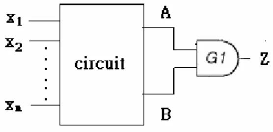
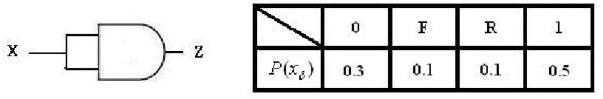
(27) the gateY is defined as: Y [ xiα ]. (i = 1, 2,… , n; α = 0,1) ,. where Y [ xiα ] is derived in the following Shannon expansion: Y = xi0Y [ xi0 ] + xi1Y [ xi1 ] . Definition 2.7 (Cofactor Probability): If Y = f ( x1 , x2 ,… , xn ) is Boolean function, the cofactor probability of the gate Y is defined as : P (Y [ xiα ]) (i = 1, 2,… , n; α = 0,1) . Definition 2.8 (BAM data structure): For any node in a circuit, the BAM data. structure of this node is its signal probability and cofactor probabilities .. By BAM data structure, we could use the first order of Taylor expansion to get the difference between P( A ∩ B) and P( A) P( B) .. 2.4.2.1 2-Input AND Gate Case We take a 2-input AND gate for example to explain how they are implemented. Suppose A and B are the inputs and Z is the output of a 2-input AND gate in Figure 2-1, thus we have Z = AB . The difference between P ( AB ) and P ( A) P( B) represents. the signal correlation effects. We can get. P ( AB) = P( Z ) ≈ P ( A) P( B) + ∑ P ( xi ) P( xi ) × ( P( A[ xi0 ]) − P( A[ xi1 ]) ) × ( P( B[ xi0 ]) − P( B[ xi1 ]) ) n. i =1. and P( AB[ xiα ]) = P( Z [ xiα ]) ≈ P( A[ xiα ]) P( B[ xiα ]) .. (Equation 2-1 and Equation 2-2). Figure 2-1: 2-input AND gate with n primary inputs.. In the equation P ( AB) = P( A) P( B) + ∑ P( xi ) P( xi ) × ( P( A[ xi0 ]) − P( A[ xi1 ]) ) × ( P( B[ xi0 ]) − P( B[ xi1 ]) ) , n. i =1. 17.
(28) the first term of right-hand side of the equation is obtained by considering A and B are mutually independent. The second term is considered as a sum of the correction terms to the first term. These correction term pull-back real number calculation to Boolean algebraic calculation. In fact, for example, these correction terms replace P ( xi ) P ( xi ) contained in P ( A) P( B) by 0 in accordance with the fact xi xi = 0 in the Boolean algebra. These operations correct the difference of the multiplication law between Boolean algebra and real number, e.g. xi xi = xi ( xi xi = 0 ). (. ). and P ( xi ) P ( xi ) ≠ P ( xi ) P ( xi ) P( xi ) ≠ 0 . To proof the equation mentioned above, suppose A and B are logic functions of mutually independent Boolean variables x1 , x2 ,… , xn .The can be expressed formally in the form of sum of product, for example 1. 1. xα ∑ ∑ α α. A=. 1. 1 =0. 1. n =0. xnα n A[ xα ] ,. where BAM have defined α ≡ (α1 ,… , α n ) and A[ xα ] is either 0 or 1 for each α . The similar equation also holds for B as B=. 1. 1. xβ ∑ ∑ β β. xnβn B[ x β ] ,. 1. 1 =0. n =0. 1. The probability that the logic value of A equals to 1 and B equals to 1 are obtained as follows: P ( A) =. 1. P ( xα ) ∑ ∑ α α 1. 1 =0. P( B) =. 1. 1. n =0. 1. 1. P( x β ) ∑ ∑ β β 1. 1 =0. n =0. 1. P( xnα n ) A[ xα ] , P( xnβn ) B[ x β ] .. The product of P ( A) and P( B) can be expressed as follows: where ηiαβ ≡ P( xiα ) P( xiβ ) (i = 1,… , n; α , β = 0,1) , 18. P( A) P( B) = F (η ).
(29) F (ξ ) ≡ ∑∑ ξ α1β1 α. ξ. αn βn. A[ xα ]B[ x β ]. β. On the other hands, since the form of sum of products for the Boolean product of A and B is such that AB ≡ ∑∑ x1α1 x1β1 α. xnα n xnβn A[ xα ]B[ x β ]. β. The probability that the logic value of AB equals to 1 can be expressed as follows:. P( AB) = F ( χ ) where χ iαβ ≡ P( xiα xiβ ). (i = 1,… , n; α , β = 0,1). Note that P ( AB) and P ( A) P( B) have been expressed by a single equation F .Therefore, P ( AB) − P( A) P( B) can be approximated by the first-order terms of the Taylor expansion of F : n. 1. 1. P ( AB ) − P( A) P ( B) = F ( χ ) − F (η ) ≈ ∑∑∑ ( χ iαβ − ηiαβ ) i =1 α = 0 β = 0. ∂F (η ) ∂ξiαβ. It’s easy to show that. χ iαβ − ηiαβ = (−1)α + β P( xi ) P( xi ) (i = 1,… , n;α , β = 0,1) and. ∂F (η ) = P( A[ xiα ]) P( B[ xiβ ]) , where [ xiα ] and[ xiβ ] are the cofactors of the αβ ∂ξi. Shannon expansions of A and B around xi respectively. As a result, we obtain the first equation of BAM: P ( AB) = P( A) P( B) + ∑ P( xi ) P( xi ) × ( P( A[ xi0 ]) − P( A[ xi1 ]) ) × ( P( B[ xi0 ]) − P( B[ xi1 ]) ) n. i =1. By taking the 0th-order Taylor expansion of the difference between P( AB[ xiε ]) and P ( A[ xiα ]) P( B[ xiα ]) , then we could obtain: P ( AB[ xiα ]) ≈ P( A[ xiα ]) P( B[ xiα ]). 19. (i = 1,… , n; α = 0,1) ..
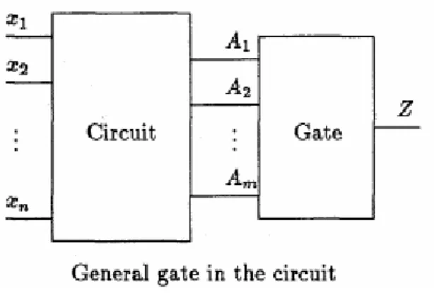
(30) According to the first equation of BAM, the necessary information at the input node, for example A, is a set of signal probability P ( A) and cofactor probabilities P( A[ xiα ])(i = 0,1,… n; α = 0,1) which is BAM data structure in definition 2.8.. 2.4.2.2. General Case. This subsection will present the application of BAM to a general logic gate such as OR, XOR, or more complicated functions. Suppose the gate under consideration has m inputs, A1 ,. , Am , and Z is one of the. outputs of the gate. Figure 2-2 is the illustration of such gate.. Figure 2-2: General case in the circuit. Shannon expansion of Z around A1 : Z = A1Z [ A1 ] + A1Z [ A1 ] gives the relation between Z and A1 . Since A1Z [ A1 ]( A1Z [ A1 ]) is the product of two logic functions A1 and Z [ A1 ] ( A1 and Z [ A1 ] ), Equation 2-1 can be applied to approximate the signal probability of Z such that P(Z ). P ( A1 ) * P ( Z [ A1 ]) + P( A1 ) * P( Z [ A1 ]). The Cofactor probabilities at node Z are obtained in the same manner as follows: 20.
(31) P ( Z [ xiα ]). P( A1[ xiα ]) * P( Z [ A1 ][ xiα ]) + P( A1[ xiα ]) * P( Z [ A1 ][ xiα ]) (i = 1,. , n; α = 0,1). According to equation 2-13 and 2-14, the BAM data structure at node Z is obtain from those for A1 , A1 , Z [ A1 ] , and Z [ A1 ] . The BAM data structure for A1 is easily obtained from that for A1 , while those for Z [ A1 ] and Z [ A1 ] are obtained by recursive Shannon expansion around A2 ,. An .. Equations 2-1 and 2-2 imply that the approximate signal and cofactor. probabilities for the gate output Z are obtained from those for the gate inputs immediately without knowledge about the previous circuit.. 2.4.3 Algorithm of BAM The signal probabilities at all circuit nodes can be calculated by means of the following algorithm: I.. Set BAM data structures for the primary inputs.. II.. Extract a gate such that BAM data structures for its inputs are already calculated but those for its outputs are nod yet calculated. If such gate does not exist, then exit.. III. Calculate the BAM data structures for the gate outputs from those for the gate inputs by using Equations 2-1 and 2-2 IV. Go to II.. 2.4.4 Switching Activities BAM also could be used to the switching activity calculation. But it is more complicated than to the signal the temporal correlation of the identical primary input. Assume A , B , C and D are logic function of primary inputs. The first fundamental. 21.
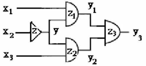
(32) equation is as follows: P ( A(τ ) B (0)C (τ ) D(0) ) n. P ( A(τ ) B(0)) P(C (τ ) D(0)) + ∑. i =1 (. ∑ββ αα ′)<(. ′). piαα ′ piββ ′ × ( X iαα ′ − X iββ ′ ) × (Yiαα ′ − Yi ββ ′ ) (Equation 2-3). def. def. def. def. where (00) = 0, (01) = 1, (10) = 2, (11) = 3, def. piαβ = P( xiα (τ ) xiβ (0)), def. X iαβ = P( A[ xiα ](τ ) B[ xiβ ](0)), for and α , β = 0,1 .. and. def. Yiαβ = P(C[ xiα ](τ ) D[ xiβ ](0)), The Second fundamental equations are as follows:. P ( AC[ xiα ](τ ) BD[ xiβ ](0) ). (i = 1,. P( A[ xiα ](τ )) P( B[ xiβ ](0)) × P(C[ xiα ](τ )) P( D[ xiβ ](0)) ,. , n; α , β = 0,1). (Equation 2-4). 2.4.5 Example In this section, we take the circuit in Figure 2-3 for an example to see how BAM is implemented to calculate switching activities at each node level by level: Example 2.2. Figure 2-3: A test circuit.. There are some basic values of the circuit in Figure 2-3: P ( x1 ) = 0.5; P( x2 ) = 0.5; P ( x3 ) = 0.5.. Psw ( x1 ) = 0.1; Psw ( x2 ) = 0.2; Psw ( x3 ) = 0.1.. Then we could use this information to do calculation. Level 0: The BAM data structures for the primary inputs are set as follows: 22.
(33) If i = j then. i.. P ( xi [ xαj ](τ ) xi [ x βj ](0) ) = 1 , for α and β =1. P ( xi [ xαj ](τ ) xi [ x βj ](0) ) = 0 ,else. If i ≠ j then. ii.. P ( xi [ xαj ](τ ) xi [ x βj ](0) ) = P ( xi (τ ) xi (0) ) = P( xi ) − 0.5 × Psw ( xi ) , n; α , β = 0,1). (because xi and x j are mutually independent) (i = 1, P ( x1[ x10 ](τ ) x1[ x10 ](0) ) = 0, P ( x1[ x11 ](τ ) x1[ x11 ](0) ) = 1,. e.g.. P ( x1[ x20 ](τ ) x1[ x20 ](0) ) = P ( x1 (τ ) x1 (0) ) = 0.5 − 0.5 ⋅ 0.1 = 0.45. Level 1: The BAM data structure for node y is obtained from those at level 0 as. Psw ( y ) = Psw ( x2 ) = 0.2 P ( y[ xiα ](τ ) y[ xiβ ](0) ) = P ( x2 [ xiα ](τ ) x2 [ xiβ ](0) ) , (i = 1,. , n; α , β = 0,1) .. e.g. P ( y[ x20 ](τ ) y[ x20 ](0) ) = P ( x2 [ x20 ](τ ) x2 [ x20 ](0) ) = 0. Level 2: The BAM data structure for node y1 is obtained from those at level 0 and. level 1 as follows:. ( (. ) (. )). ) (. Psw ( y1 ) = 2 ⋅ P x1 (τ )x1 (0) y (τ ) y (0) + P x1 (τ )x1 (0) y (τ ) y (0) + P x1 (τ ) x1 (0) y (τ ) y (0) = 0.14. (. P x1 (τ )x1 (0) y (τ ) y (0). (. ). ). 3. = P x1 (τ )x1 (0) P ( y (τ ) y (0) ) + ∑. i =1 (. ( (. P ( xα (τ ) xα (0) ) P ( x β (τ ) x β (0) ) ∑ αα ββ ′. ′)< (. i. ′). i. ′. i. i. )) (. ) (. × P x1[ xiα ](τ ) x1[ xiα ′ ](0) − P x1[ xiβ ](τ ) x1[ xiβ ′ ](0) × P ( y[ xiα ](τ ) y[ xiα ′ ](0) ) − P ( y[ xiβ ](τ ) y[ xiβ ′ ](0) ). (. ) (. ). The calculation of P x1 (τ )x1 (0) y (τ ) y (0) , P x1 (τ ) x1 (0) y (τ ) y (0) is similarly. P ( y1[ xiα ](τ ) y1[ xiβ ](0) ) ≈ P ( x1[ xiα ](τ ) x1[ xiβ ](0) ) ⋅ P ( y[ xiα ](τ ) y[ xiβ ](0) ). 23. ).
(34) (i = 1,. , n; α , β = 0,1). and BAM data structure for node y2 is obtained similarly. Level 3: The BAM data structure for node y3 is obtained from those at level 2 as. follows:. ( (. ) (. )). ) (. Psw ( y3 ) = 2 ⋅ P y1 (τ ) y1 (0) y2 (τ ) y2 (0) + P y1 (τ ) y1 (0) y2 (τ ) y2 (0) + P y1 (τ ) y1 (0) y2 (τ ) y2 (0) = 0.088. (. P y1 (τ ) y1 (0) y2 (τ ) y2 (0). (. ). ). 3. = P y1 (τ ) y1 (0) P ( y2 (τ ) y2 (0) ) + ∑. ∑. i =1 (αα ′ ) < ( ββ ′ ). ( (. P ( xiα (τ ) xiα ′ (0) ) P ( xiβ (τ ) xiβ ′ (0) ). ) (. )) (. × P y1[ xiα ](τ ) y1[ xiα ′ ](0) − P y1[ xiβ ](τ ) y1[ xiβ ′ ](0) × P ( y2 [ xiα ](τ ) y2 [ xiα ′ ](0) ) − P ( y2 [ xiβ ](τ ) y2 [ xiβ ′ ](0) ). (. ) (. ). The calculation of P y1 (τ ) y1 (0) y2 (τ ) y2 (0) , P y1 (τ ) y1 (0) y2 (τ ) y2 (0) is similarly. P ( y3[ xiα ](τ ) y3 [ xiβ ](0) ) ≈ P ( y1[ xiα ](τ ) y1[ xiβ ](0) ) ⋅ P ( y2 [ xiα ](τ ) y2 [ xiβ ](0) ). (i = 1,. , n; α , β = 0,1). In this example BAM gives the exact signal probability for node y3 . The exact signal probability at node y3 can be derived by: Psw ( y3 ) = Psw ( ( x1 x2 )( x2 x3 ) ) = Psw ( x1 x2 x2 x3 ) = 0.088. BAM could estimate the switching activities at all nodes in a combinational logic circuit with relative accuracy and without constructing global BDDs. It uses the concept of Taylor expansion to get the first order signal dependence effects due to reconvergent fan-out nodes are taken into account. Further more, it take the temporal correlation among the primary input in estimating switching activities, but ignore spatial correlation.. 2.5 Real-Delay Boolean Function (RDBF) Considering for glitches generation again, a glitch is generated at the output of a gate, if the following conditions are met: 24. ).
(35) i.. The necessary condition, which requires the difference of the arrival times of the input signals to be greater than the inertial delay of the gate.. ii.. The sufficient condition, which requires the appropriate transitions of the input signals(s) to switch the gate output.. Consequently, the timer parameter plays a critical role in the power consumption estimation. Hence, the exact description of a logic circuit should include not only its logic signals. Furthermore, since the glitch generation is strongly dependent on time, a modified Boolean function — real delay Boolean function (RDBF), which describes the logic and timing behavior of each signal, is needed. Example 2.3 We assume the logic circuit of Figure 2-4, where the gate delays are. multiples of reference delay unit d .. Figure 2-4: A logic circuit with non-zero delay gates.. The logic behavior of the node f can be described in time domain by the following RDBF: f = F ( x1 , x2 , t ) = x1 (t − 5d ) x2 (t − 5d ) x2 (t − 3d ) (Equation 2-1). The signal f may switch at two time instances, i.e. t1f = 3d and t2f = 5d . More specifically, the transition of the signal f at t1 , t1f = 3d , depends on the transitions of the primary inputs x1 and x2 at time points t1x1 = −2d , t1x2 = −2d , and t1x2 = 0 . The corresponding Boolean function is f1 = x1 (−2d ) x2 (−2d ) x2 (0) .. 25.
(36) The transition of f at t2f = 5d depends on the transition of the signal x1 and x2 at t2x1 = 0 and t2x2 = 0 , while the corresponding Boolean function is f 2 = x1 (0) x2 (0) x2 (2d ) .. Thus, the behavior of the signal f is described in time domain by the corresponding RDBF. Moreover, the RDBF of f is reduced to ordinary Boolean function f1 and f 2 , whose variables are the logic values of the input signals at specific time instances. Also, since node f may perform transitions at t1f = 3d and t2f = 5d , evaluation the transition activity of function f1 , f 2 the transition activity of the RBDF is also evaluated. For us, we take FR-Vector to process glitches, and combine it with BAM to consider the correlations. In original BAM, it must be operated in a zero-delay model. .For this, we need to add the delay information into BAM by real delay Boolean function. We would discuss it in detail in next chapter.. 26.
(37) Chapter 3 FR-Vector with BAM 3.1 Review and Integration The goal of this paper is to propose a new technique which could analyze switching activity, and further more, signal correlations and glitches processing are included. In section 2.3 , we introduce FR-vector. It could be used in a non-zero delay model and it could also process glitch activity. In additional, while most papers use complex equations to calculate switching probability, FR-vector simplifies the calculations of switching probability as the calculations signal probability. As we can see, though there are many advantages in FR-vector, the signal correlations are not included in FR-vector. The other techniques we talked in section 2.4 is Boolean approximation method, it uses Taylor expansion to approximate the difference between two probabilities P( A) and P( B ) multiplied immediately and the real probabilities as they intersected- P ( A ∩ B) . BAM indeed is a data structure, which could be used to calculate the difference mentioned above. BAMs are used to pass through the circuit and calculate the signal (or switching) probability of nodes in the whole circuit. In BAM, it solves the correlations due to reconvergent circuit by the concept of Taylor expansion. Another advantage of BAM is it doesn’t need to construct OBDD of the circuit, so it is faster than many other techniques which processing reconvergent circuits. Unfortunately, the delay model use in BAM is zero-delay model. Without delay information of the circuit, the activity of glitches would be ignored too. The ability of glitch processing in FR-Vector, and the ability of signal correlations processing in BAM both are what we want. So, in this thesis, we try to 27.
(38) combine these two techniques as a new model, and call it as FR-Vector with BAM.. 3.2 Basic Definition and assumption FR-Vector wit BAM is a non-zero delay model in inertial mode. It has an assumption: z. Mutual independency of the primary inputs.. This assumption is gotten from the original first assumption in BAM, and we eliminate the second assumption to fit with FR-Vector. The inertial model is the basic condition in FR-Vector. As in FR-Vector, we will sample a signal line S n times in a clock cycle, then divide a clock cycle into n states (state = 0,1 ). Then, using the sampled rule to get FR-Vector ( n frames a vector, each frame = 0, F , R,1 ). From FR-Vector, we could get FR-Matrix ( 4 × N matrix. Each column in the matrix represents a frame with the same index, and the entries in the 4 rows will be used to represent the occurrence probability of 0, 1, R, and F in that frame, respectively.). Following is the explanation of the meaning of FR-Matrix in FR-Vector with BAM: Definition 3.1 (Switching signal):In FR-Vector with BAM, the ith frame, xt =i , in. FR-Vector is called the switching signal in time i . (0 < i < n − 1) Definition 3.2 (Switching probability): In FR-Vector with BAM, the ith frame in. FR-Matrix is called the switching probability in time i , and denoted as P ( xt =i ) , ( x = 0, F , R,1 ; 0 < i < n − 1) . In FR-Vector with BAM, we also used a data structure to carry the information of correlation among the circuit. Recall the cofactor probability used in section 2-4, we also have cofactor transition relation in FR-Vector with BAM. The differences are: I.. We add the concept of “frame” as a basic time unit in place of “clock”.. II.. The BAM data structures in FR-Vector only exist in nodes which are in 28.
(39) reconvergent part of the circuit. Definition 3.3 (Cofactor Transition Relation): If Y = f ( x1, x2,…, xn ) is Boolean function,. and we having m frames in a clock cycle. The cofactor transition relation of it are defined as:. ( ) ]) = P (Y [ x ](t )Y [ x ](t − 1) ) ]) = P (Y [ x ](t )Y [ x ](t − 1) ). P (Y f0 [ xiαβ ]) = P Y f [ xiα ](t )Y f [ xiβ ](t − 1) P (Y fF [ xiαβ P (Y fR [ xiαβ. α. f. i. β. f. α. f. i. i. β. f. (i = 1, 2,… , n ; α , β = 0,1 ; 0 < f < m − 1 ). i. P (Y f1[ xiαβ ]) = P (Y f [ xiα ](t )Y f [ xiβ ](t − 1) ). which means the probabilities of cofactors remains 0, transition from1 to 0, transition from 1 to 0, and remains 1 at frames f respectively. Definition 3.3 (Reconvergent circuit): A reconvergent circuit is a circuit which. convergent in a specific node and some signal lines in this circuit has forked before its convergent node. Definition 3.4 (Supply set of the reconvergent circuit): A supply set S X of a. reconvergent circuit X is a set of nodes {s1 , s2 ,… , sn } , which si is the input of reconvergent circuit X. There is an example of supply set: Example 3.1 There is a circuit likes Figure 3-1:. 29.
(40) Figure 3-1: An example of supply set of the reconvergent circuit: In reconvergent circuit X , the supply set of. X is { x4, w, x7 , y2 } .. In figure 3-1, there is a reconvergent circuit X = {w, x4 , x7 , y, y2 , y3 } in circuit S , and the supply set of X is { x4, w, x7 , y2 } . Definition 3.5 (Cofactor Transition Relation Matrix): A cofactor transition relation matrix is a three dimension matrix of nodeY . (A 4 × f × n matrix, n is the. number of nodes of the reconvergent circuit which node A is belonged to, and f is the number of frames.) Each item in the matrix denotes the cofactor transition relation P (Yt γ [ xiδ ]) of node Y where δ , γ = 0, F , R,1 ; 0 < t ≤ f − 1 ; and 0 < i ≤ n . Definition 3.6 (The BAM data structure of FR-Vector): For any node belonged to a. reconvergent in a circuit, the FR-Matrix and the cofactor transition matrix of this node is called its BAM data structure of FR-Vector. Because of the assumption - “ Mutual independency among primary input”, each pair of nodes which are not in the reconvergent circuit or they are in the supply set of a reconvergent circuit, would be taken as independent. By this, we could get: Theorem 3.1 : The BAM data structures of a node xi , xi ∈ S and S = {x1 , x2 ,… , xn } is. a supply set of the reconvergent circuit, could be gotten as: (i). If i = j , P( xδi [ xγj ]) = 1 , when δ = γ , P ( xδi [ xγj ]) = 0 , when δ ≠ γ .. (ii). If i ≠ j , P ( xδi [ xγj ]) = P( xδi ) . ( 0 < i ≤ n − 1 ; δ , γ = 0, F , R,1 ). Now, we know how to sample the signal as FR-Vector and get FR-Matrix of primary inputs. In further more, we can use theorem 3.1 to get their BAM data structures if it is in reconvergent circuit. In next section, we talk about how to 30.
(41) propagate these information gate by gate, and from primary inputs to the output of the circuit.. 3.3 Probabilities Propagation In convenient to introduce FR-Vector with BAM, we start in zero-delay model, we will extend FR-Vector with BAM to non-zero delay model in section 3.6. In order to analyze the probabilities at each node in the circuit, we divide the circuit into two parts: z. General circuit, and. z. Reconvergent circuit.. In general circuit, we do not use BAM data structure. Because of the assumption “Mutual independence among the primary input”, if there is no reconvergent circuit, there is no correlation among circuit too. For this reason, it is redundant to calculate and propagate the BAM data structure in these circuits. Indeed, in non-reconvergent circuit, even if we still use the BAM data structure in it, it would do nothing. We leave the explanation of this later in section 3.3.2. Without BAM data structures, our model is simplify to original FR-Vector, so we could propagate FR-Matrix as it propagates in original FR-Vector. In the other case, reconvergent circuit, we will set up BAM data structure using theorem 3.1 in the supply set of the reconvergent circuit. Then we need to propagate these BAM data structure to calculate the other nodes which is not in supply set in the reconvergent circuit, including cofactor transition relation and FR-Matrix.. 3.3.1 Propagation of the Cofactor Transition Relation Before talking about the propagation of the cofactor transition relation, we should discuss the real significance in it. The cofactor comes from Shannon expansion. Suppose the gate under consideration has m inputs, A1 , outputs of the gate. Shannon expansion of Z around A1 is. Z = A1Z [ A1 ] + A1Z [ A1 ] ,. 31. Am , and Z is one of the.
(42) and thus. P ( Z ) = P ( A1 ) P ( Z [ A1 ]) + P( A1 ) P( Z [ A1 ]) . We could say that a cofactor P( Z [ xi ]) is the probability of Z is logic high when xi is logic high. As the same concept, we could get:. If there is a gate whose inputs are ( x1 , x2 ,… , xn ) and one of its output. Lemma 3.1. is Z , we take the cofactor transition relation P ( Zδ [ xαi ]) as the probability of transition δ (δ = 0, F , R,1) happens at output Z when the transition of its input xi is α (α = 0, F , R,1) . Theorem 3.2 : If there is a gate whose inputs are A and B , the circuit it belonged to. has the primary input set {x1 , x2 ,… , xn } , and a clock cycle is divided into m frames, then we have: P ( Aαf [ xiδ ] ∩ B βf [ xiδ ]). (. = P Af B f [ xiδτ ](τ ) Af B f [ xiδ0 ](0) δτ. ). δ0. P( Af [ xi ](τ ) Af [ xi ](0)) × P( B f [ xiδτ ](τ ) B f [ xiδ 0 ](0)). ,. (Equation 3-1). = P( Aαf [ xiδ ]) P ( B βf [ xiδ ]). (i = 1,. , n; δ = 0, F , R,1; δτ , δ 0 = 0,1; f = 1,. , m). Proof: The proof of this theorem is similar to equation 2-4 in section 2.4, we get the equation 3-1 in the same way as how we get equation 2-4. The difference is we add the concept of “frame”.. By lemma 3.1, we could use the logic composition table (Table 3-1) as FR-Vector used to propagate FR-matrix to propagate the cofactor transition relation. To explain how to use these tables, we take an example as below: Example 3.2 There is an AND gate whose inputs are a, b and output is c ,the primary. inputs is ( x1 , x2 ,… , xn ) , and there are m frames in a clock cycle. Thus, according to table 3.1(a) we could get. 32.
(43) P (c 0f [ xiα ]) = P (a 0f [ xiα ]) × P (b 0f [ xiα ]) + P (a 0f [ xiα ]) × P (b Ff [ xiα ]) + P (a 0f [ xiα ]) × P(b Rf [ xiα ]) + P (a 0f [ xiα ]) × P(b1f [ xiα ]) + P(a1f [ xiα ]) × P(b 0f [ xiα ]) + P( a Ff [ xiα ]) × P(b0f [ xiα ]) + P(a Rf [ xiα ]) × P(b 0f [ xiα ]) + P( a Rf [ xiα ]) × P(b Ff [ xiα ]) + P (a Ff [ xiα ]) × P (b Rf [ xiα ]) P (c Ff [ xiα ]) = P(a1f [ xiα ]) × P(b Ff [ xiα ]) + P( aF [ xiα ]) × P(b Ff [ xiα ]) + P( a Ff [ xiα ]) × P(b1f [ xiα ]). \ Table 3-1:. The composition table for cofactor transition relation.. P (c Rf [ xiα ]) = P(a1f [ xiα ]) × P(b Rf [ xiα ]) + P( a Rf [ xiα ]) × P(b Rf [ xiα ]) + P(a Rf [ xiα ]) × P(b1f [ xiα ]). and P (c1f [ xiα ]) = P(a1f [ xiα ]) × P(b1f [ xiα ]) .. (0 < i < n − 1; α = 0, F , R,1; 1 < f < m − 1) For example, if we want to get the probability of transition F happens at output c when the transition of node xi is α , that is P(c Ff [ xiα ]) .We should know c Ff [ xiα ] will happen at time a1f [ xiα ] ∩ b Ff [ xiα ] , a Ff [ xiα ] ∩ b Ff [ xiα ] , and a Ff [ xiα ] ∩ b1f [ xiα ] ( where Aδf [ xiα ] means node transition δ happens at node A at the time the transition of xi is α in time frame 33.
(44) f ). So we could get P (cF [ xiα ]) = P(c Rf [ xiα ]) = P(a1f [ xiα ] ∩ b Rf [ xiα ]) + P(a Rf [ xiα ] ∩ b Rf [ xiα ]) + P(a Rf [ xiα ] ∩ b1f [ xiα ]). 3.3.2 Propagation of the FR-Matrix In FR-Vector with BAM, we also use logic composition table to propagate the FR-Matrix, but the difference is when the node is in a reconvergent part of the circuit. That is, in the original FR-Vector, we get the FR-Matrix of an output from its immediate inputs. It comes from two items in each matrix of the input multiplied immediately, and without considering signal correlation due to reconvergent circuit. Though there may be distance between two probabilities multiplied immediately and the real probability it will be, the original FR-Vector ignores this. Take a simple example to see how the reconvergent circuit affects the transition probability:. Example 3.3 Figure 3-2is a simple reconvergent with input node x , and output. node z . The right table is the FR-Matrix of node x .. Figure 3-2: A reconvergent circuit and the FR-Matrix of its input node x.. In this circuit, the signal will diverge from node x , and reconvergent at node z . If we use the original FR-Vector to calculate the transition probability of node z as its transition is 1, it will be P ( z1 ) = P ( x1 ) × P( x1 ) = 0.5 × 0.5 = 0.25 . Indeed, the real probability is P ( z1 ) = P ( x1 ) = 0.5 . As mentioned before, considering for the correlation due to reconvergent, we use 34.
(45) BAM to handle it. Replace the calculation- P ( Aα ∩ B β ) = P( Aα ) P( B β ) in the original FR-Vector (that is, multiplying two items in different FR-Matrices), we have: Theorem 3.3 : At the convergent node of a reconvergent circuit, if there is a gate. whose inputs are A and B , the circuit it belonged to has the primary input set {x1 , x2 ,… , xn } , and a clock cycle is divided into m frames, then we have:. (. P ( Aδf ∩ Bγf ) = P Aδf τ (τ ) Bγf τ (0) Aδf 0 (τ ) Bγf 0 (0) n. ). P( Aδf ) P( Bγf ) + ∑ ∑ pi f pi f × ( X i f − X i f ) × (Yi f − Yi f ) α. β. α. β. α. β. ,. (Equation 3-2). i =1 α < β. def. α. α. pi f = P( xi f ) def. def. def. def. where (0) = 0, ( F ) = 1, ( R) = 2, (1) = 3,. α. def. α. and X i f = P( Aδf [ xi f ]), α. def. α. Yi f = P( Bγf [ xi f ]) ( δ , γ , α , β = 0, F , R,1; f = 0,. m; δτ , δ 0 , γ τ , γ 0 = 0,1; i = 1,. , n .). Proof: The proof of this theorem is similar to equation 2-3 in section 2.4, we get the equation 3-2 in the same way as how we get equation 2-3. The difference is we add the concept of “frame”.. In equation 3.2, the second item of right-hand side n. ∑ α∑β p i =1. <. α. if. β. α. β. α. β. pi f × ( X i f − X i f ) × (Yi f − Yi f ) is the difference we used to modify the. original equation in FR-Vector. Recall the example 3.3, if we used FR-Vector with BAM to calculate P ( z1 ) , it would be P ( Z 1 ) = P( x1 ∩ x1 ) P( x1 ) P( x1 ) + ∑ ∑ pi pi × ( X i − X i ) × (Yi − Yi ) α. β. α. β. α. β. x1 α < β. = ( P( x )) + ∑ P( xα ) P( x β ) × ( P( x1[ xα ]) − P ( x1[ x β ])) × ( P( x1[ xα ]) − P( x1[ x β ])) 1. 2. α <β. = ( P( x )) + 1. 2. ∑. P( xα ) P( x β ) × ( P ( x1[ xα ]) − P( x1[ x β ])) × ( P ( x1[ xα ]) − P ( x1[ x β ])). (α , β ) = (0,1),(1,2),(1,3). 35.
(46) = ( P( x1 )) 2 + P( x 0 ) P ( x1 ) × ( P ( x1[ x 0 ]) − P( x1[ x1 ])) × ( P ( x1[ x 0 ]) − P( x1[ x1 ])) + P( x1 ) P ( x 2 ) × ( P ( x1[ x1 ]) − P ( x1[ x 2 ])) × ( P ( x1[ x1 ]) − P ( x1[ x 2 ])) + P( x1 ) P ( x 3 ) × ( P( x1[ x1 ]) − P( x1[ x3 ])) × ( P( x1[ x1 ]) − P( x1[ x 3 ])) = ( P( x1 )) 2 + P( x 0 ) P ( x1 ) + P( x1 ) P( x 2 ) + P( x1 ) P( x3 ) = 0.25 + 0.03 + 0.03 + 0.05 = 0.36. In the beginning of this section, we have mentioned: Theorem 3.4 : The process of BAM data structures in non-reconvergent will do. nothing in the propagation of switching probability. Proof:. For each gate in non-reconvergent circuit, we divide them into two cases: The inputs of the gate is primary input:. (i). α. β. α. β. ( X i f − X i f ) × (Yi f − Yi f ) α. β. α. β. = ( P( Aδf [ xi f ]) − P ( Aδf [ xi f ])) × ( P( Bγf [ xi f ]) − P( Bγf [ xi f ])) , where this equation is. extract form equation 3.2. From theorem 3.1 and A ≠ B , there must be one of. {( X. α if. β. α. β. }. − X i f ), (Yi f − Yi f ) would be 0,. (for there must be A ≠ xi or B ≠ xi ) n. Thus, the difference equation ∑ ∑ pi f pi f × ( X i f − X i f ) × (Yi f − Yi f ) will be 0. α. β. α. β. α. β. i =1 α < β. (ii). The input of the gate is not primary input:. Because the gate is in a non-reconvergent circuit, the transition of a node X would be independent of the primary input xi . α. β. α. β. Thus we can get P ( Aδf [ xi f ]) = P( Aδf [ xi f ]) , and Bγf [ xi f ]) = P ( Bγf [ xi f ]) , α. β. α. β. ( X i f − X i f ) × (Yi f − Yi f ) α. Then,. β. α. β. = ( P( Aδf [ xi f ]) − P( Aδf [ xi f ])) × ( P( Bγf [ xi f ]) − P( Bγf [ xi f ])) = (0) × (0) =0 36.
(47) n. Thus, the difference equation ∑ ∑ pi f pi f × ( X i f − X i f ) × (Yi f − Yi f ) will be 0. α. β. α. β. α. β. i =1 α < β. From (i) and (ii), we could get the conclusion that, BAM data structures in non-reconvergent will do nothing in the propagation of switching probability Beside we do not propagate the switching probability in non-reconvergent; we only calculate the switching probability at the node where reconvergent circuit is converged for there is only this node would be affected by reconvergent correlation. Thus, we use FR-Vector among the whole circuit, and use BAM data structures in the reconvergent part of the circuit and propagate them gate by gate until the convergent node, but Lemma 3.2. We only use BAM data structure to calculate the switching probability. at convergent node of a reconvergent circuit. Again, we discuss how these BAM data structures solve the correlations caused by reconvergent circuit. Let’s survey the proof of equation 3-2 firstly. A part of proof of equation 3-2:. If P( xδf ) is the probability of the transition δ happens in the f th frame of x, then let P( Aδf ) × P( Bγf ) = F (η ) ,. where def. ηiαβ = P ( xiα f ) P( xiβ f ) (i = 1,. , n; α , β , γ , β = 0,1, 2,3; 0 ≡ 00,1 ≡ 01, 2 ≡ 10,3 ≡ 11). and def. F (ξ ) = ∑∑ ξ1α1β1 α. def. ( α = (α1 f ,. β. ξ nα β A[ xα f ]B[ x β f ] n n. , α n f ) , and A[ xiα f ] is either 0 or 1 for each α ).. The Boolean product of Aδf and Bγf is such that 37.
(48) Aδf Bγf = ∑∑ x1α1β1 f α. xnα n βn f A[ xα f ]B[ x β f ] ,. β. the probability that the logic value of Aδf Bγf equals to 1 can be expressed as follows: P( Aδf Bγf ) = F ( χ ) def. where χ iαβ = P( xiα f xiβ f ) (i = 1,. n; α , β = 0,1, 2,3) .. Note that P( Aδf Bγf ) and P( Aδf ) P( Bγf ) have been expressed by a single function F . Therefore, P ( Aδf Bγf ) − P( Aδf ) P( Bγf ) can be approximated by the first-order terms of the Taylor expansion of F : P ( Aδf Bγf ) − P ( Aδf ) P( Bγf ) = F ( χ ) − F (η ) n. 3. ∂F. 3. ( χ αβ − η αβ ) αβ (η ) ∑∑∑ ∂ξ α β i =1. where. =0. =0. i. ,. i. i. ∂F (η ) = P( A[ xiα f ]) P( B[ xiβ f ]), and A[ xiα f ] and B[ xiβ f ] are the cofactor αβ ∂ξi. translation relation of the Shannon expansions of A and B around xi respectively. Thus, ( χ iαβ − ηiαβ ). ∂F (η ) = ( P( Aδf Bγf ) − P( Aδf ) P( Bγf ) ) × P( A[ xiα f ]) P( B[ xiβ f ]) . αβ ∂ξi (Equation 3-3). From the right-hand side of (Equation 3-3, we could get the physical meaning of equation 3-2. For the equation 3-3 means the effect do to transition at node A and node B caused by input variables xiα f and xiβ f . We could see 3. ∂F. 3. ( χ αβ − η αβ ) αβ (η ) ∑∑ ∂ξ α β =0. =0. i. i. n. node xi f , and. is the summation of the effect caused by all transition at. i. 3. ∂F. 3. ( χ αβ − η αβ ) αβ (η ) ∑∑∑ ∂ξ α β i =1. =0. =0. i. i. is the summation of all effect caused by. i. input variables. Thus equation 3-2 means the equation P( Aδf Bγf ) is approximating to P( Aδf ) P( Bγf ) add the effect caused by input variables. Further more, for the cofactor 38.
(49) is generated by the characteristic of circuit and its structure. The effect calculated by equation 3-2 could catch the effect due to different types of circuit structure, thus the reconvergent circuit. A node’s cofactor transition relation represents the meaning of how each primary input affect the transition in node itself. Thus, in reconvergent circuits, we propagate this information to the immediate inputs of the convergent node, and use equation 3-2 to correct the switching probability in convergent node. Why this equation could do correction. It’s because when we use the logic composition table and FR-Matrices of inputs to compute the FR-Matrix of output node, equation 3.2 could correct the differences between the probability of two event happened in the same time (what we need) and the probability of two probabilities of event multiplied immediately(two terms in logic composition table multiplied immediately). The correction is gotten from the effect due to primary inputs which has been recorded in cofactor transition relation as we have explained above.. 3.4 An Example of FR-Vector with BAM In previous section, we have a tiny attempt in FR-Vector in BAM. In this section, we try to use a simple and more complete example to show the propagation of the FR-Vector with BAM in reconvergent circuit. Example 3.4 There is a simple reconvergent circuit, and Table 3-2is its switching. probabilities in each input nodes.. 39.
數據


+7

相關文件
Wang, Solving pseudomonotone variational inequalities and pseudocon- vex optimization problems using the projection neural network, IEEE Transactions on Neural Networks 17
Then, we tested the influence of θ for the rate of convergence of Algorithm 4.1, by using this algorithm with α = 15 and four different θ to solve a test ex- ample generated as
Numerical results are reported for some convex second-order cone programs (SOCPs) by solving the unconstrained minimization reformulation of the KKT optimality conditions,
Particularly, combining the numerical results of the two papers, we may obtain such a conclusion that the merit function method based on ϕ p has a better a global convergence and
Then, it is easy to see that there are 9 problems for which the iterative numbers of the algorithm using ψ α,θ,p in the case of θ = 1 and p = 3 are less than the one of the
By exploiting the Cartesian P -properties for a nonlinear transformation, we show that the class of regularized merit functions provides a global error bound for the solution of
Define instead the imaginary.. potential, magnetic field, lattice…) Dirac-BdG Hamiltonian:. with small, and matrix
A convenient way to implement a Boolean function with NAND gates is to obtain the simplified Boolean function in terms of Boolean operators and then convert the function to
