g 行政院國家科學委員會補助專題研究計畫
□ 成 果 報 告
■期中進度報告
高效能可程式化之三維電腦繪圖多媒體晶片系統-子
計畫七:支援三維電腦繪圖多媒體晶片系統多頻多電
壓之電路設計(1/3)
計畫類別:□ 個別型計畫 ■ 整合型計畫
計畫編號:NSC 96-2220-E -110-008-
執行期間: 2007 年 8 月 1 日至 2008 年 7 月 31 日
計畫主持人:郭可驥
共同主持人:
計畫參與人員: 徐亦璽、施明宏、蔡逸星
成果報告類型(依經費核定清單規定繳交):□精簡報告 ■完整
報告
本成果報告包括以下應繳交之附件:
□赴國外出差或研習心得報告一份
□赴大陸地區出差或研習心得報告一份
□出席國際學術會議心得報告及發表之論文各一份
□國際合作研究計畫國外研究報告書一份
預定六月國際學術會議 International Conference on IC Design and
Technology June 2-4, 2008 Minatec in Grenoble, France 發表 A
Low Power Multi-band Selector DLL with Wide-Locking Range
處理方式:除產學合作研究計畫、提升產業技術及人才培育研究
計畫、列管計畫及下列情形者外,得立即公開查詢
□涉及專利或其他智慧財產權,□一年□二年後可公
開查詢
執行單位:國立中山大學資訊工程學系
中 華 民 國 97 年 5 月 24 日
可供推廣之研發成果資料表
□ 可申請專利 □ 可技術移轉 日期: 年 月 日國科會補助計畫
計畫名稱: 計畫主持人: 計畫編號: 學門領域:技術/創作名稱
發明人/創作人
技術說明
中文: (100~500 字) 英文:可利用之產業
及
可開發之產品
技術特點
推廣及運用的價值
※ 1.每項研發成果請填寫一式二份,一份隨成果報告送繳本會,一份送 貴單位研發成果推廣單位(如技術移轉中心)。 ※ 2.本項研發成果若尚未申請專利,請勿揭露可申請專利之主要內容。 ※ 3.本表若不敷使用,請自行影印使用。 附件二中文摘要
近幾年來無線通訊產品均走向體積小、低耗能以及性能佳等特性發展,於是 積體化電路及 SOC(System on chip)的發展以成為主流,使得時脈產生、接收發 機的需求量大增,大多使用鎖相迴路(Phase-locked loop, PLL)以及延遲鎖定迴 (Delay-locked loop, DLL)。也因為無線通訊產品的普及,不斷的有人投入在鎖 相迴路(Phase-locked loop, PLL)以及延遲鎖定迴路(Delay-locked loop, DLL) 的研究與製作,連帶的越來越多鎖相迴路(Phase-locked loop, PLL)以及延遲鎖 定迴(Delay-locked loop, DLL)的應用於是產生,如應用在 3D 繪圖晶片設計。 頻率合成器在通訊及系統的應用中扮演著了極為重要的角色,PowerPC
System-on-a-Chip 之頻率合成器通常使用鎖相迴路(PLL,Phase Locked Loop) 技 術 以 提 供 系 統 一 個 頻 率 穩 定 且 準 確 之 本 地 振 盪 訊 號 (Local Oscillator frequency)。對於目前在此PowerPC System-on-a-Chip系統而言,具有切換速度 快、相位雜訊低、頻率解析度高以及消耗功率低的PLL可以有效提昇系統性能, 尤其是以利用相位及頻率作調變的系統,如PowerPC SOC等,更是明顯而有迫切 的需要。對一頻率合成器而言,提升切換速度並降低訊號相位雜訊的最主要方法 是盡量減少除頻數以增加鎖相迴路頻寬,使其能有效抑制在迴路頻寬內電壓控制 振盪器之相位雜訊,並且減少相位元頻率偵測器(Phase Frequency Detector) 及除頻器(Divider)等之雜訊增益。本子計劃提供多重頻率產生器(系統時脈、 智財時脈、記憶體時脈、影像時脈、外部時脈輸出) ,支援三維電腦繪圖多媒體 晶片系統。
Abstract
The wireless communication products have moved towards the characteristic such as being good of small, low consuming energy and performance to develop in recent years, then integrated circuit and SOC (System on chip) Development in order to become mainstream, the demand for making the pulse generator, transceiver is heightened, mostly use Phase-locked loop (PLL) And Delay-locked loop (DLL). Because the popularization of the wireless communication products too, research which someone constant puts into in PLL and DLL and making, then the application of related more and more PLL and DLL is produced, for example apply it to 3D chip while designing .
Frequency Synthesizer plays an extremely important role in the communicational and systematic application. Frequency Synthesizer of PowerPC System-on-a-Chip usually uses PLL as a stable and accurate frequency. As far as the system of PowerPC System-on-a-Chip us concerned, it can be switched quickly, its Phase has low noise, its resolution of frequency is high, and the low power supply can efficiently enhance the function of the system. For example, PowerPC SOC and the like especially use Phase and frequency as the system of modulation, which is obviously an urgent need. For Frequency Synthesize, the main method of increasing the switching speed and lowering the noise of Phase is to lower Divider so as to increase the bandwidth of PLL, thereby efficiently preventing the noise of Phase in the loop Frequency VCO and decreasing the sounds in Phase Frequency Detector and Divider. This project generates Multi-frequency Clock Generator (for system clock, IPs clocks, memory clocks, video clock, external clock output, etc), and support the need in the Low-Power Circuit Design Supporting Multi-Frequency Multi-Voltage for 3D Graphics and Multimedia SoC
Preface
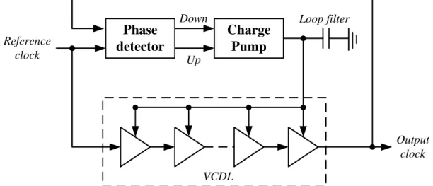
Design of advanced digital systems requires a fully understanding of clock management circuits. The synchronous design methodology is built on the premise of a reliable clock distribution scheme. High performance applications require new clock management approaches to keep synchronous circuit functioning properly. Synchronous design is popular because it simplifies timing relationships, allowing the designer to focus on circuit functionality. The only performance concerns with synchronous designs are maximum clock frequency and input and output timing relationships. Management of chip-level clock skew is typically handled by careful layout of the integrated circuit (IC) device. Several techniques are available, including buffered-tree, clock-grid, and clock-tree synthesis approaches. The buffered tree is routinely used on FPGA devices because the register clock multiplexer input pins create a fixed, regular load. Clock-tree synthesis is popular in ASIC designs because it optimizes performance, power, and area. In fact, management of board-level skew can be even more difficult than managing chip-level clock skew. As faster technologies have become available, it has become necessary to use phase-locked loop (PLL) and delay-locked loop (DLL) circuits to minimize skew. Elements that exhibit significant delay are put inside of a feedback loop, such that the effective delay can be minimized or nulled. With proper design in the DLL, the overall system clock skew can be minimized.In several 3-D graphics uses a power management by Dynamic Voltage and Frequency Scaling (DVFS) system for power saving. In DVFS system, there are two standard approaches for finding minimum energy point. The one uses the tracking table, the other uses the load modeling VCO. The clocking methodology of the present microprocessor handles such challenges by radically departing from a single chip-wide clock distribution, to better control clock skew, jitter and power consumption. Using one simple ring type phase-locked loop for the local reference clock, several delay-locked loops to clock separate the 3-D graphic section. The following figure shows diagramed the concept.
Therefore, the circuit design of this project is divided into two parts. The first part is DLL and second part is PLL.
Table of contents
Part I : DLL
CHAPTER 1
CHAPTE 1 Introduction 7
CHAPTER 2 Concepte pf Delay-Locked Loop 9
CHAPTER 3 A Low Power Multi-band Selector DLL with Wide-Range Locking and Simulation Results/Conclusion 20
Reference 41
Part II: PLL
CHAPTER 1 Motivation 43CHAPTER 2 Introduction of structure 44
CHAPTER 3 Simulation Results/Conclusion 51
Reference 59
Part I
CHAPTER 1
Introduction
1.1 Motivation
In many clock applications delay-locked loop (DLL) and phase-locked loop (PLL), are widely used for high-speed synchronization system, communication interface, memory system, and clock buffer. Design of advanced digital systems requires a fully understanding of clock management circuits. The synchronous design methodology is built on the premise of a reliable clock distribution scheme. High performance applications require new clock management approaches to keep synchronous circuit functioning properly. Synchronous design is popular because it simplifies timing relationships, allowing the designer to focus on circuit functionality. The only performance concerns with synchronous designs are maximum clock frequency and input and output timing relationships. In digital system application, there are several problems known as jitter makes phase-locked loop (PLL) susceptible to supply voltage, ground noise and clock skew which is the signal variations becomes large. As faster technologies have become available, it has become necessary to use phase-locked loop (PLL) and delay-locked loop (DLL) circuits to minimize skew. Elements that exhibit significant delay are put inside of a feedback loop, such that the effective delay can be minimized or nulled. With proper design in the DLL, the overall system clock skew can be minimized. In the conventional delay-locked loop (DLL) design, the component called the voltage-controlled delay line instead of the voltage-controlled oscillator in the PLL. The advantage of the voltage-controlled delay line is that it dose not accumulate the noise injection. In general, the DLL usually is used by a capacitor in the loop filter which is unconditional stable because it belong the first order system.
1.2 Research Objectives
As the CMOS process technology has developed rapidly in recent years, the chip size and clock frequency grow. The speed performance of very large scale integrated (VLSI) system increase speedy, and it is important to suppress skew and jitter in the clock systems. The block of the conventional DLL composed of phase frequency detector (PFD), charge pump (CP), loop filter (LP), voltage-controlled
delay line (VCDL), and other additional circuit which like low dropout regulator, calibration circuit. Each block has some problem on themselves, for example, phase frequency detector (PFD) has dead-zone problem, the charge injection and current mismatch in the charge pump (CP), the voltage-controlled delay line (VCDL) is constricted by frequency range, and other circuit may increase the overall system unstable factor. Moreover, the charge pump transfer function is found to be low-pass while the voltage-controlled delay line transfer function is high-pass with equal bandwidth. This exposes a bandwidth tradeoff that restricts the designer. In this project, we focus the objectives are:
I. How to extend the frequencies range of the delay-locked loop (DLL). II. The jitter performance and relationship between the loop bandwidth.
III. How to avoid the impact of power supply noise and substrate noise in the digital and analog circuit.
IV. To overcome process, voltage, and temperature (PVT) variations in the proposed system.
CHAPTER 2
The Concepts of Delay-locked Loop
2.1 DLL Overview
The delay-locked loop (DLL) have been widely employed in memory interface, communication ICs and microprocessors due to generator the on-chip clocks. DLLs also are used to produce multiphase clock signals for clock generator, clock buffer and skew suppression. The DLL is able to adjust only phase between the reference clock and the output clock, not frequency. After the phase alignment process is finished, the voltage-controlled delay line (VCDL) generates a stable clock signal. Unfortunately, there are some non-ideal phenomenon in each block of the DLL.
As mention above, the main problem of the DLL is that they are vulnerable to the process variations, supply voltage, and temperature variations (PVT). It makes designer hard to design a pure clock source. For example, if we want to make the low-jitter performance, we must set the lower loop bandwidth of the DLL loop configuration. However, it makes the longer acquisition time due to small loop bandwidth. On the other hand, the higher loop bandwidth can benefit faster locking time, but it leads to large jitter. In next section, we will introduce the basic principle of the DLL system.
2.2 Operation Principle and DLL components
The conventional delay-locked loop (DLL) consist a phase frequency detector (PFD) or phase detector (PD) which is only compared with phase, charge pump (CP), loop filter (LF) that is usually made a single capacitor, and the voltage-controlled delay line (VCDL). Figure 2.1 shows a basic block diagram of the conventional DLL. The reference clock is fed to phase detector (PD) and voltage-controlled delay line (VCDL) which outputs clock. The phase detector detects the phase error between reference clock and output clock of the VCDL, which is generates a pulse signal Up and Down. The Up signal is the reference clock leads the output clock, the Down signal vice verse. The charge pump input signal is controlled by Up and Down signal of the phase detector, respectively. The charge pump is based on the pulse width to generate the corresponding current, thus it can charge or discharge for the loop filter. The following VCDL is controlled by a filtered control voltage Vctrl and adjusts the reference clock phase, then fed back to PD, requesting new phase detection again.
2.3 Phase Detector / Phase Frequency Detector
The goal of the phase detector is to compare phase error between input clock and output clock. Therefore, the PD produces an output signal proportional to the phase difference of the signal applied to its inputs. The simplified PD consists of
EXOR which is illustrated in Figure 2.2. As the phase difference varies, the output pulse width will be changed. Thus provides a dc level proportional to △ψ. A conventional phase detector has been two major concerns, including the dead-zone problem and the operation frequency which is importance of the DLL system. There are usually used to detect the minimum phase different and to verify the performance of PD. The operation frequency is an important factor in DLL due to the feedback path doesn’t have divider to reduce the operation frequency. In Figure 2.3 shows a transfer curve of PD, which is also shows a dead-zone phenomenon. The conventional phase frequency detector (PFD) is illustrated in Figure 2.4. This PD is composed of two D flip-flop (DFF) and a AND gate. An all of the logic gates are static logic. These
Figure 2.1 Basic block diagram of the conventional DLL
two DFF input “D” are settled to “high” and the AND gate output connects to “reset” of 1 1 Reset Reset D D CLK CLK Up Down A B Up Down B A
the DFF. In the figure 2.4 (b) shows a timing diagram of the conventional PFD. When A-phase leads B-phase, the A-phase is rising to the edge trigger of the DFF and produces an Up pulse and until the B-phase also rising to the edge trigger, the Up and Down pulses are “high” at the same time. It reset those two DFF which outputs to “low”.
2.3.1 Recent research of PD and PFD
In conventional PD, additional delay to avoid dead-zone problem which increase the longest delay path. It will limit the highest operation frequency. To solve the problems of speed limitation and dead-zone problem, a new type phase detector used the dynamic logic is adopted. Figure 2.5 (a) shows the circuit of the dynamic CMOS phase detector [1]. This half-transparent (HT) register consists of six transistors and the dynamic CMOS phase detector composes by two HT registers. This simple phase detector is improved by no reset path, it can speed up the operation frequency and reduces the influence of the dead-zone. Figure 2.5 (b) describes the timing diagram. If the ref_clk leads the VCDL_clk, then the HT register produces a pulse width “Up” between ref_clk and the VCDL_clk, and the other outputs signal “Down” outputs low.
Figure 2.4 (a) the conventional PFD (b) timing diagram
Ref_clk VCDL_clk Ref_clk VCDL_clk Up Up Down Down
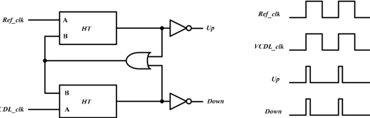
A new type phase frequency detector also uses the dynamic logic, which is similar to the dynamic PD. This dynamic PFD is shown in figure 2.6. It adds an OR gate to the reset path. The shorted feedback delay path improves the speed limitation. In order to avoid the dead-zone problem, when the ref_clk and VCDL_clk at the same phase, the PFD produces the Up and Down signals with an equal pulse width to set the charge pump. The charge pump does not act for this input signal. If there is phase difference between ref_clk and VCDL_ref, the width of the output signal will be proportional to the phase differences [2].
Figure 2.5 (a) the schematic of the dynamic phase detector (b) timing diagram (a)
2.4 Charge Pump and Loop Filter
The two digital signals produced by a PFD have to be converted back into an analog control signal at the input of the VCDL, and the most commonly used to perform this job is called a charge pump. The charge pump is made of two controllable current source connected to a capacitor which is called loop filter, shown in figure 2.7. The outputs from the PFD turn one of the two switches, which either charge or discharge to the loop filter (LF). The charge pump is the analog component of the DLL that will be considered.
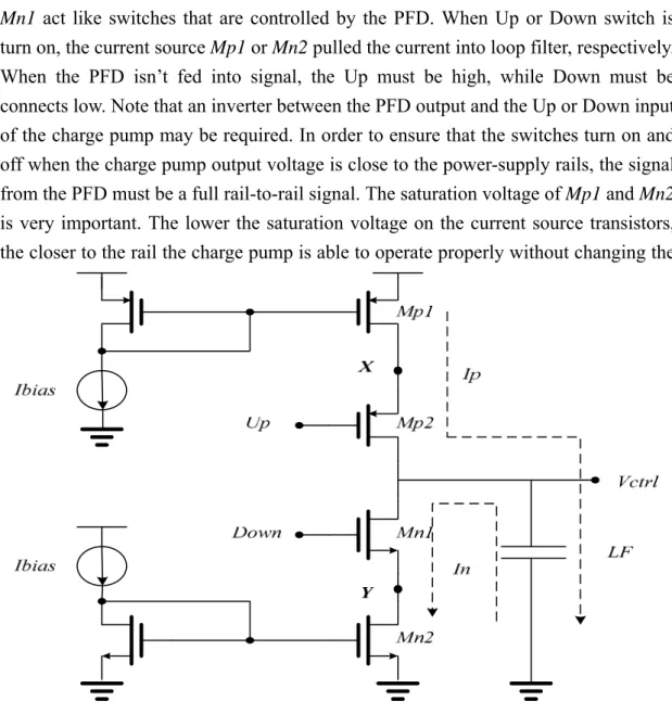
The design of charge pump must be very carefully due to there are non-ideal phenomenon, such as leakage current, current mismatch, clock feed-through, and charge sharing from the switches, dead-zone in the PFD, and so on. Figure 2.8 is the single-end charge pump circuit. This charge pump consists of four transistors Mp1 through Mn2. The transistor Mp1 and Mn2 act as current source, and the Mp2 and
Figure 2.6 The block diagram of PFD and its timing diagram
Mn1 act like switches that are controlled by the PFD. When Up or Down switch is
turn on, the current source Mp1 or Mn2 pulled the current into loop filter, respectively. When the PFD isn’t fed into signal, the Up must be high, while Down must be connects low. Note that an inverter between the PFD output and the Up or Down input of the charge pump may be required. In order to ensure that the switches turn on and off when the charge pump output voltage is close to the power-supply rails, the signal from the PFD must be a full rail-to-rail signal. The saturation voltage of Mp1 and Mn2 is very important. The lower the saturation voltage on the current source transistors, the closer to the rail the charge pump is able to operate properly without changing the
loop gain, therefore , the loop dynamics. The loop filter uses a single capacitor due to the DLL system usually uses the first order configuration.
2.4.1 Programmable Bias Schemes
Often it is desirable to be able to adjust the current flowing in the charge pump either because the designer would like the flexibility of being able to adjust the loop bandwidth or because the exact charge pump current for the best phase noise performance is not known with certainty before fabrication. The wide-range DLL has large gains of the VCDL. The current of the charge pump also influences the loop bandwidth. The charge pump current can easily be made scalable with a simple circuit shown in figure 2.9 [3]. The current of the charge pump is determined by the digital control signal B1 and B2.
Ibias Res Down Up B1 B2 B1 B2 LF Vctrl
2.5 Voltage-controlled Delay Line
Variable delay elements are often used to manipulate the rising or falling edge of the clock or other pulse in integration circuit. In variable delay element, the delay between the rising/falling edge of the output and that of input can be varied. This delay can be changed by either analog or digital means. In analog means, an analog controlling voltage or current allows us to achieve desired delay. On the other hand, discrete voltage or capacitor allows manipulation of the delay through digital means in digitally controlled delay elements. Inverter chain and RC delay method have been the most common delay elements in those applications. Both of them are simple and easy to design. However, the characteristics of the delay elements are sensitive to environmental conditions such as supply voltage and ambient temperature. Attempts to find a less delay element less sensitive to supply voltage and temperature variations have been made [4]-[5]. A differential stage chain provides stable characteristics but consumes static power, requires a complex biasing circuitry for delay variation, and, in general, is not feasible to implement a large delay value with different stages. Biasing techniques with feedback mechanism can enhance the figure of sensitivity. However, such approaches cannot compensate high frequency perturbation as the power line noise, which causes meta-stability in synchronous system. In all the above-mentioned category of delay elements, the delay element is one of the crucial
components and its precision directly affects the overall performance of the circuit. In figure 2.10 shows a basic voltage-controlled delay line.
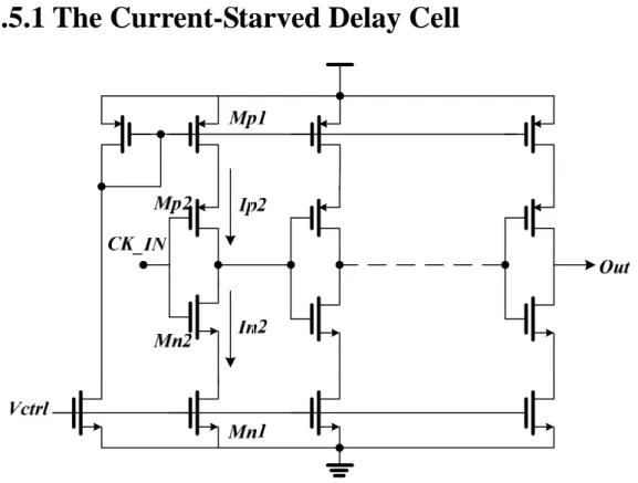
2.5.1 The Current-Starved Delay Cell
Figure 2.11 shows a schematic of the current-starved controlled delay element. The transistors Mp2 and Mn2 operate as an inverter, while transistors Mp1 and Mn2 operate as current source. The current source Mp1 and Mn1, limit the current available to the Mp2 and Mn2. The amount of output current is decided by the current source
Mn1 and the Mn1 controlled by the voltage, Vctrl. If the voltage of Vctrl is a small
amount or quantity, while the Mn1 outputs small amount of current. The Mp1 is similar to Mn1. The single-end delay element, costs less active area and power dissipation. However, it is vulnerable to power supply noise and substrate noise. Therefore, the low noise differential delay element is needed. In next section, we will introduce a low noise differential delay element.
Figure 2.10 A basic voltage-controlled delay line
2.5.2 Differential delay elements with symmetric loads
The figure 2.12 shows a schematic of the differential delay element with symmetric loads [6]. The delay element contains a source coupled pair with resistive load elements called symmetric loads. Symmetric load consists of a diode-connected PMOS device in shunt with an equally sized biased PMOS device. The PMOS bias voltage VBP in nominally equal to Vctrl, the control input to the bias generator. Because of this equality, Vctrl will be used instead of VBP in subsequence references to the PMOS bias voltage. Vctrl define the lower voltage swing limit of the buffer outputs. The buffer delay changes with Vctrl since the effective resistance of the load elements also changes with Vctrl. It has been shown that these load elements lead to good control over delay and high dynamic supply noise rejection. The simple NMOS current source is dynamically biased with VBN to compensate for drain and substrate voltage variations, achieving the effective performance of a cascade current source. However, this current source can provide high static supply and substrate noise rejection without the extra supply voltage required by cascade current sources.
Figure 2.12 Differential delay elements with symmetric loads
In figure 2.13, the buffer bias current is 2Id. It can be show that the effective resistance of a symmetric load R is directly proportional to the small signal resistance at the ends of the swing range which is just one over the transconductance gm for one of the two equally sized devices when biased at VBP or, equivalently, Vctrl. The symmetric load has a good linearity and the I-V cure is symmetric at the center of output swing. Because the nonlinear load resistance usually converts the common mode noise into differential mode noise, the symmetric load has high supply noise rejection. Vctrl Vout_N Vout_P Vin_N Vin_P Mp1 Mp1 Mp2 Mp2 Mn1 Mn1 Mb1
This circuit schematic of the wide-range tuning delay cell is shown in figure 2.14 [7]. The delay cell consists of one NMOS input pair Mn1, one PMOS positive feedback pair Mp1, and one PMOS transistor Mb1 for frequency tuning. In high-frequency operation, an NMOS input pair is used to maximize the transconductance-to-capacitor (gm/C) ratio to achieve high operating frequency with low power dissipation. Only parasitic capacitors of devices are utilized. In wide frequency-tuning range, a large tuning range is required to overcome the problem of process variation. The operating frequency can be tuned by a variable capacitor or by load impedance. In this design, frequency tuning is achieved by tuning the transconductance (gm) of the diode-connected PMOS devices Mp2. By controlling the current of Mb1, gm of Mp2 can be adjusted from zero to a value close to gm of Mp1. In low noise performance, the source nodes of devices Mp1, are directly connected to supply to eliminate current limitation of the output nodes and thus maximize output amplitude. Since output becomes large, transistors are turned off periodically. As shown in figure 2.15, noise current Nn1, Np1, Np2 is zero when output amplitude is
large. The carrier power is increased and the noise power is reduced simultaneously. Vout_N Vin_P Mp1 Mp2 Mn1 Mb1 Vout_P Vctrl Vout_P Vout_N Vin_P Nn1 Np1 Np2 Nb1
CHAPTER 3
A Low Power Multi-band Selector DLL
with Wide-Range Locking
In this chapter, a delay-locked loop of multi-band selector with wide-locking range and low power dissipation is presented. The architecture of the proposed delay-locked loop consists of phase frequency detector, charge pump, band selector, multi-controlled delay line, and start-up circuit. The multi-band selector is used to extend operation frequency of delay-locked loop by switching the multi-controlled delay line. By using multi-band technology the proposed DLL can provide wider range and lower jitter compared to those of other method. The operation frequency can be ranged from 250MHz to 900MHz. The static phase error is 6.75ps and 23.65ps at 250MHz and 900MHz, respectively. The maximum locking time is about 115 clock cycles at 250MHz. The power dissipation is 14.5mW at 900MHz. The circuit design with HSPICE simulation is using TSMC 0.18-um single-poly and six-metal CMOS process with 1.8V supply voltage.
3.1 Introduction
In recent years, wireless communication products focus on reducing the size of chip and lowering the power consumption while still maintain the same performance requirement. The integrated circuit and System on chip (SOC) becomes the mainstream of development. The clock generator is one of the major building blocks in the SOC. Generally, in the high performance applications, such as microprocessor [8], memory circuit [9], and wireless communication IC’s [10], Delay-Lock Loop (DLL) has better performance compared to that of Phase Lock Loop (PLL). For the conventional PLL the jitter performance is poorer compared to that of DLL, and the system must to wait for a longer settling time. Most clock generators in high-performance microprocessor employ a phase-locked loop (PLL), which includes a voltage-controlled oscillator (VCO). The PLL is a higher order system and is difficult to design. Its loop bandwidth, which is critical for stable operation, can be changed due to process, voltage, and temperature (PVT) variation. In the PLL, the VCO output timing uncertainty accumulates over multiple oscillation cycles and is limited by the time response of the PLL. State-of-art microprocessor operates under increasingly more noisy conditions and suffers from the delay variation due to
significant power supply/substrate noises. The delay variations cannot be corrected instantaneously by the PLL [11].The DLL is a first-order system and is always stable and, thus, easier to realize on digital circuit. It occupies smaller area and consumer less power.
Unfortunately, the requirement of the increased operation frequency limits the usage of conventional DLL. Some solutions are presented in [12]-[16]. In [12], the frequency multiplier uses an edge combiner to combine the output frequency. This special edge combiner using LC-tanks is designed to enhance the load impedance. However, it wastes a large die area to constitute the LC-tanks. A digital logic gate combiner is used to multiply the output frequency [14]. It uses less area and power dissipation compared with LC-tanks. In [15], it uses VCO to generate a multiplier frequency signal, and cut off the oscillator loop by N reference clock periodically. The advantage of this architecture is the improved cycle to cycle jitter compared to that of using edge combiner. A mixed analog and digital circuit DLL is proposed in [16]. The digital part of the VCDL utilizes a 2-bit SAR algorithm to speed up the lock time.
3.2 Locking Problem of Conventional DLL
Phase detector Charge Pump Reference clock Output clock Loop filter VCDL Down Up
A simplified block diagram of the conventional DLL is illustrated in figure 3.1. This circuit contains a voltage-controlled delay line (VCDL), a phase detector, a charge pump, and the first-order loop filter. The delay line consisting of a cascaded variable delay stages, is driven by input reference clock. The output of the delay line’s final stage and the reference clock falling edges are compared by the phase detector to determine the phase alignment error. The phase detector output is integrated by the charge pump and loop filter capacitor to generate the control voltage, Vctrl, of the delay stage. A conventional DLL may lock or attempt to lock to an incorrect delay. If the delay different from integer multiples of clock period is detected, the closed loop
will automatically correct it by changing the delay time of the VCDL. However, the conventional DLL will fail to lock or falsely lock to two or more periods, Tclk, of the input signal if the initial delay of the VCDL is shorter than 0.5Tclk or longer than 1.5Tclk, as shown in Figure 3.2 [17]. Therefore, if the DLL is required to lock the delay to one clock cycle of the input reference signal, the initial delay of the VCDL needs to be located between 0.5Tclk and 1.5Tclk, regardless of the initial voltage of the loop filter.
3.2.1 Harmonic Locking and Stuck Looking
Figure 3.2 Normal lock and false lock conditions in conventional DLL
Figure 3.3 Three stage of VCDL outputs at (a) correctly locking (b) harmonic (a)
The mean of the harmonic locking problem is that the PD locks at two or more cycles as shown in figure 3.3 (b). When the PD in the comparison point, it detects between input reference clock and output clock of the final delay stage. The output clock of the final delay stage is exceeding the 1.5Tclk, make the PD detects at two or more period and the system is in locking state. In figure 3.3 (b), the VCDL has two period delay, in other words, the VCDL locking process is locked at the harmonic of input reference clock. The harmonic locking of delay-locked loop which output phase could be non-monotonic. In other words, the output phase is not in sequence. In the multiphase application, we expected that the total delay of the delay line must be equal one period of the input reference clock. Figure 3.3 (a) shows a locking processor at one period exactly. However, in the synchronous digital system, the zero, two or more delay is still feasible.
Another possible situation for the false locked is the stuck locking. If the maximum delay of the VCDL is smaller than the half period of input reference clock, 0.5Tclk, the phase detector which detects output clock of the VCDL is always lagging the input reference clock, and decreases the control voltage to VCDL. Therefore, the DLL would try to lock a zero delay as shown in figure 3.3 (c). However, .the VCDL delay time could not be zero, and the rising edge of VCDL output clock could never lock to be original. Therefore, the DLL would be stuck at this situation. The frequency range of the input signal in which the DLL operates normally can be derived from the following two criterions. First, if the maximum and minimum delays of VCDL are TVCDL,max and TVCDL,min, respectively, the input signal should satisfy equation (3-2) and
(3-3). ,min VCDL T < TCLK < TVCDL,max (3-1) CLK T < TVCDL,max< 3 2 × TVCDL,max (3-2) 1 2 × TCLK < TVCDL,min< TCLK (3-3)
Base on equation (3-1) ~ (3-3), the range of stuck-free clock period should satisfy the following inequality:
max {TVCDL,min, 3
2 × TVCDL,max} < TCLK < min {2TVCDL,min,TVCDL,max} (3-4)
If the TVCDL,max > 3TVCDL,min, it would be no solution, and TVCDL,max ≤ 3TVCDL,min,
3.3 Propose Structure and its Operation Principle
The characteristic of conventional DLL is shown in figure 3.4. If the Vctrl increase to the maximum then the VCDL would be delayed to minimum and vice versa. In the discussion before, the initial delay of the VCDL needs to between 0.5Tclk and 1.5Tclk, no matter what initial voltage of the loop filter is. If we want to satisfy this equation under any condition, while it can still achieve to wide range operation. Therefore, we provide a method to solve this problem, and its concept is shown in figure 3.5.
The concept of solving the range problem is to make many KVCDL of the VCDL.
This method is widely used in phase-locked loop (PLL) [18]. Figure 3.5 (a) shows an ideal transfer curve. This curve is similar to resistance characteristic of MOSFET in
Figure 3.4 The transfer curve of conventional VCDL
Figure 3.5 (a) multi-KVCDL of ideal VCDL (b) multi-KVCDL of non-ideal VCDL
ideal environment. The real situation of the MOSFET does not always operate in triode range as shown in figure 3.5 (b). When the drain of PMOS inputs low voltage (at GND) is in saturation state and the NMOS is so forth.
Using of the multi-KVCDL can provide low jitter performance due to the small
KVCDL of VCDL by the influence of noise. Conventional DLLs with wide operating
range are vulnerable to the noise in the voltage-controlled delay line (VCDL) or on the control voltage because their wide-range resulting from the increase of the delay range of the VCDL for a limited range of the loop filter (LF). Thus, this leads to large jitter [19].This method must be carefully designed to avoid losing lock in gap between each of VCDL curve. Therefore, it needs to overlap some area in each adjacent VCDL curve. For example, the upper boundary of line 2 must be higher than the lower boundary of line 1 and the lower boundary of line 2 must be lower than the upper boundary of line 3. Overlapping area should be able to designed avoid false lock due to the process variation.
Figure 3.6 shows the architecture of the proposed DLL. It consists of six major blocks: start-up circuit, charge pump (CP), phase frequency detector (PFD), multi-control delay unit (MCDU), band selector (BS), and loop filter (LF). In [18], it uses many small VCO gains (Kvco) to avoid a high turning gain that usually decreases the sensitivity to the supply noise. In order to extend the operation frequency range of the proposed DLL use four VCDL gain (KVCDL). As mentioned
above, four KVCDL gains are controlled by digital signal (SW1, SW2). These digital
signals switch the proper positions of the delay range in the MCDU which is shown in figure 3.7. The control voltage (Vctrl) is compared with VH and VL on BS stage. The control signals are determined by BS. The VH and VL are extra input voltage. The
values are determined by the following inequality (3-4). In figure 3.7, the control voltage of the equation (3-4) needs to fall into the range between VH and VL, or the system will fail to lock. In the initial state, the start-up circuit raises the control voltage of the loop filter to VDD, and sets the VCDL to minimum delay state to avoid the harmonic locking. However, the BS is not ready to submit a correct digital signal to MCDU, because of the Vctrl at VDD, making the control voltage higher than VH. When the PFD produces phase error to discharge control voltage, Vctrl falls below the
VH voltage that the digital signal is in a stable state. If it cannot lock in this state, the
BS will change to next state for another comparison.
00 01 10 11
V
HV
LVtuning
3.4 Circuit Design
The blocks of the proposed DLL consist of phase frequency detector, charge pump, multi-controlled voltage delay line, band selector, and start-up circuit. The circuit designs of these blocks described in following sub section.
3.4.1 Phase Frequency Detector
The first block is phase frequency detector. The PFD capture wider range of (-2π , +2π ) compared with other phase detectors [17], a phase frequency detector is used to determine lock time. It compares the phase between input reference and output clock. The conventional PFD has a drawback of the dead-zone problem and speed limitation. The proposed PFD uses true single-phase clock (TSPC) D flip-flop which is composed by dynamic CMOS logic [20].
Ref_clk out_clk Up Down Ref_clk out_clk Up Down
Figure 3.8 (a) shows a timing diagram of conventional PFD. It generates an undesired glitch because of a dead-zone problem. The proposed PFD composes of four half-transparent (HT) registers and a NOR gate as shown in figure 3.9 [20]. This PFD can remove the unnecessary glitch as shown in figure 3.9 (b) and reduce the impact of dead-zone.
The main structure uses a tri-state PFD, the half-transparent (HT) registers use TSPC dynamic logic. Therefore, the proposed PFD can operate in high-speed frequency and used fewer number of transistors which can reduce delay time of the reset path. Figure 3.10 shows simulation result.
Figure 3.8 Timing diagram of (a) Conventional PFD (b) Proposed PFD
(a) (b)
Figure 3.9 (a) The structure of proposed PFD (b) The schematic of HT (a)
3.4.2 Charge Pump and Loop Filter
The circuit of the charge pump is shown in figure 3.11. The charge pump is controlled by digital signal that is Up and Down signal. Up and Down signals are generated by phase frequency detector, which detects phase difference between input reference clock and output clock. They control the current switches in the charge pump. The charge pump bases on the pulse width to generate the proportional current
Figure 3.10 Simulation result of the proposed PFD (a) Input reference clock lags output clock
(b) Input reference clock leads output clock
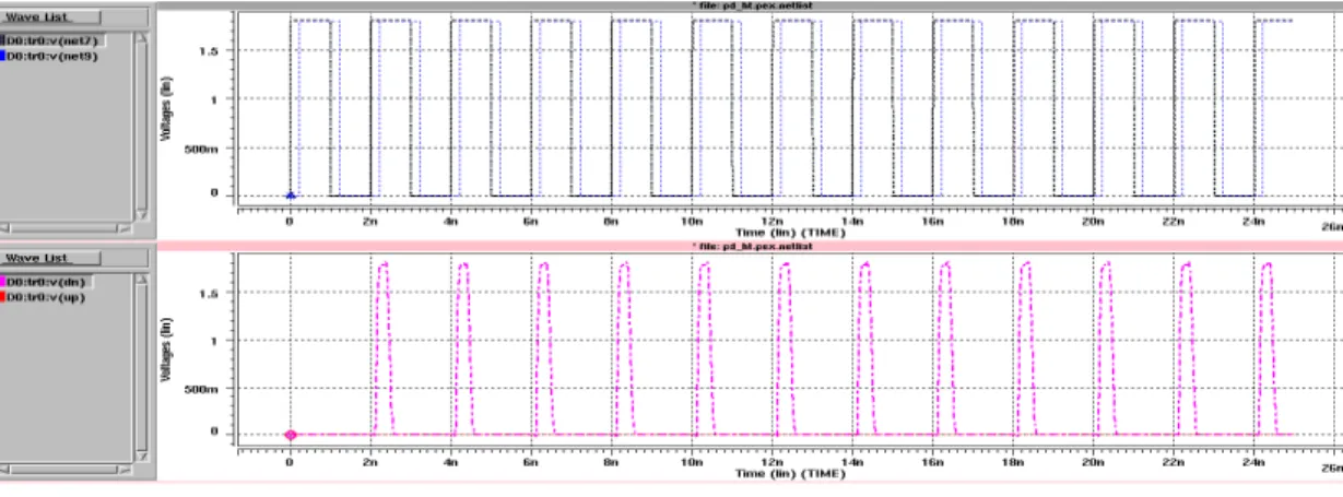
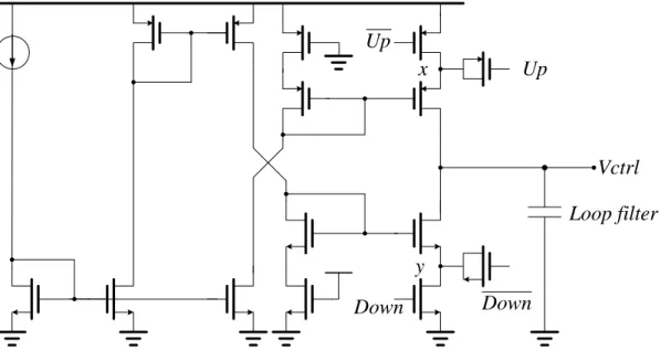
and fed to the loop filter. The problems of conventional charge pump are current mismatch and charge injection to loop filter. The charge injection contributes in node x and y. Additional capacitors are added to avoid the effect of the charge injection. In order to avoid short channel effect, the MOSFET of charge pump is slightly larger than the minimum length. Two normally turned-on NMOS and PMOS transistors are used to match bias condition when Up and Down is activated. The simulation result is shown in figure 3.12. The capacitor of loop filter is a MiM capacitor.
Vctrl Up Down Down Loop filter Up x y
Figure 3.11 The schematic of the proposed charge pump
Figure 3.12 The simulation result of charge pump (c) Up and Down
3.4.3 Start-up Circuit
DFF D Q DFF D Q Divider REF_CLK Counter_CLK Startup REF_CLK Startup TclkThe schematic of the start-up circuit is shown in Fig. 3.12 (a) [3]. It composes two rising edge trigger D-type flip-flops (D_FF) and a XOR gate. The timing diagram of the start-up circuit is shown in Fig. 3.12 (b). Initially, the output of the start-up circuit, which is generate by the rising edge of the input reference clock (ref_clk). The pulse width of output is equal to a period (TCLK) of ref_clk. The PMOS transistor of
DLL core will be turn on by this pulse and the initial control voltage of the filter will be pulled to VDD. At the same time, the delay of the multi-controlled delay cell between out_clk and ref_clk is minimum. The divider by 2 output clock is fed to counter unit. The divider by 8 output clock ensure the delay time is longer enough to rise up the loop filter at VDD in the initial time. If the loop filter does not rise up to VDD, it may occur lock false which harmonic lock.
3.4.4 Band Selector
Using smaller KVCDL can provide low jitter performance. Many of DLL and PLL
use this method [3], [18] and [21]. In [3], the DLL architecture uses the mixed-mode time-to-digital-converter scheme for a frequency-range selector. In [17], it incorporates an automatic switched-capacitor (SC) discrete-tuning loop to extend the overall frequency tuning range to 20%, while the VCO gain resulting from the CMOS varactor continuous-tuning is kept low KVCO in order to improve the reference spurs
Figure 3.12 The start-up circuit (a) The block diagram of the start-up circuit
and noise performance. In [20], the PLL architecture contains a frequency-to-voltage converter (FVC) to selector the correctly frequency-range.
In this project, we propose a simple concept of band selector. The proposed of band selector composes two voltage comparator and a down counter unit as shown in figure 3.13 (a). Band selector uses fewer digital circuits which it can provide exactly band selection. The band selector compares voltage, Vctrl, with VH and VL which both are extra input voltage. VH and VL are determined by equation (3-4). The control voltage of the equation (3-4) needs to fall into the range between VH and VL , or the system will fail to lock. In figure 3.13 (b), when the Vctrl is higher than VH, the comparator_H sends a high signal to enable the down counter to count. The counter generates 2-bit control signal (SW1, SW2) to MCDL switch the switches. If the Vctrl is lower than VH, the comparator_H will send a low signal to disable the counter and stop the counter. The comparator_L is the same but opposite operation. The down counter clock comes from start-up circuit. The frequency is reference frequency divided by two. The output signals of comparator_H and comparator_L are called VH_RST and VL_RST respectively. The reset signal is sent to PFD. If the VH_RST is High, the reference frequency signal will be reset. If the VL_RST is High, the VCDL output frequency signal will be reset. The simulation result is shown in figure 3.14 and figure 3.15.
VH
Sel
VL
Down Counter Unit E N Comparator_H
2
Vctrl CLK2 VH_RST Comparator_L VL_RST VDD GND VH VL lock Q 0 Q 1 Time Voltage 1.8 1.8 0 0Figure 3.13 The band selector block diagram and its operation (b)
3.4.5 Multi-controlled delay line (MCDU)
A signal-end delay cell is vulnerable to power supply noise and substrate noise. Differential input delay cell is used to prevent the noise injection. In the proposed DLL, the multi-controlled delay line consists of three major blocks which are analog and digital control delay line, voltage to current converter (VTC), and differential to single converter (D2S). The digital and analog control delay line is the different input delay cell. The delay line connects series with five stage delay cell as shown in 3.16 (a). The digital part of delay cell is controlled by digital signal (SW1, SW2). The digital signals produce by 2-bit down counter of band selector. The analog signal is
Vctrl voltage of the loop filter. The delay cell of the MCDU provides four different
VCDL gains. Those are K (0, 0), K (0, 1), K (1, 0), K (1, 1). The size order of KVCDL
are K (0, 0) > K (0, 1) > K (1, 0) > K (1, 1).
Figure 3.14 The simulation result of band selector (1)
As mentioned before, we talk about the principle of DLL is based on to the band selector to select suitable frequency range, then produce digital signal (SW1, SW2) to control the MCDU delay. Initially, the start-up circuit rises Vctrl voltage to VDD, when Vctrl voltage is lower than VH, the MCDU unit will be switched to K (1, 1) and start locking process. If the K (1, 1) is not in a right frequency range, it will make
Region Digital Signal Gain (KVCDL)
Range 1 Sw1=0 , Sw2=0 K(0,0)
Range 2 Sw1=0 , Sw2=1 K(0,1)
Range 3 Sw1=1 , Sw2=1 K(1,0)
Range 4 Sw1=1 , Sw2=1 K(1,1)
Table 3.1 Digital signal versus KVCDL
Figure 3.16 (a) the block diagram of MCDL (b) schematic of delay cell (a)
Vctrl voltage rise or decrease over than VH or VL. The figure 3.17 shows a flow chart
of the locking process and figure 3.18 shows a simulation result of the VCDL transfer curve.
The differential to single converter (D2S) [6] is used to convert the differential input to single output due to the delay cell used by differential input as shown in figure 3.19.The D2S also can provide 50% duty cycle output, such that the output clock can use in synchronous system. The voltage to current converter (VTC) is
Figure 3.17 The flow chart of DLL operation
widely use in PLL and DLL design. In order to make the current more linear, the VTC circuit is necessary. The figure 3.20 shows a schematic of VTC.
out IN_P
IN_N
Vbias
3.4.6 Simulation Result and Comparison
This work is simulated by using TSMC 0.18µm CMOS process. The supply voltage of the proposed DLL is 1.8V. The locking range of the proposed DLL can be ranged from 250MHz to 900MHz. The static phase error is 6.75ps and 23.65ps at 250MHz and 900MHz respectively. The maximum power consumption is 14.5mW at operation frequency of 900MHz and the maximum lock time less than 500ns. Figure 3.21 shows the lock state of 250MHz. The wave waveforms include the Vctrl voltage, reference frequency (REF), and output frequency (OUT), and SW1, SW2. Figure 3.22 shows the lock state in 900MHz. The comparison results among different designs are
Figure 3.20 The schematic of VTC Figure 3.19 The schematic of D2S
shown in the Table 3.2. It includes the power consumption, jitter performance, and the range of operation frequency. The proposed DLL exhibits a better static phase error and lower power dissipation compared to those of other related works. The detailed performance of the proposed DLL is shown in the Table 3.3 and layout is shown in figure 3.23.
Figure 3.21 The proposed DLL locking at 250MHz
[3] [16] [21] This work Process 0.25µm 0.35µm 0.35µm 0.18µm Supply voltage 2.5V 3.3V 3.3V 1.8 Operation Frequency Range 32MHz ~320MHz 6MHz ~130MHz 62.5MHz ~250MHZ 250MHz ~900MHz Static Phase Error < 39.4ps NA < 40ps < 23.65ps Power Dissipation 15mW @ 320MHz 132mW@ 130MHz NA 14.5mW @ 900MHz Lock Time 22 clock
cycles ~1130 clock cycles NA < 115 clock cycles Active Area 0.07mm^2 0.45mm^2 0.08mm^2 0.035mm^2 Specification Result Technology TSMC 0.18µm 1P6M Supply Voltage 1.8 V
Operating Frequency Range 250MHz – 900MHz Chip Area (with PAD)
Active Area
0.628 × 0.693 mm^2 0.170 × 0.209 mm^2 Static Phase Error 6.75ps @ 250MHz
23.65ps @ 900MHz Power dissipation 1.15mW @ 250MHz
14.5mW @ 900MHz Lock Time < 460ns @ 250MHz
(~115 clock cycles)
Table 3.2 Performance comparison
Additional work is simulated by using UMC 90-nm CMOS process. The supply voltage of the proposed DLL is 1V. The locking range of the proposed DLL can be ranged from 33MHz to 333MHz. The maximum power consumption is 8.32mW at operation frequency of 333MHz and the maximum lock time less than 1us. Figure 3.24 shows the lock state of 33MHz. The wave waveforms include the Vctrl voltage, reference frequency (REF), and output frequency (OUT), and SW0, SW1. Figure 3.25 shows the lock state in 333MHz.
Figure 3.24 The proposed DLL locking at 33MHz Figure 3.23 The layout of proposed DLL
Figure 3.25 The proposed DLL locking at 333MHz
Conclusion:
A novel delay-locked loop is presented. The multi-band selector is used to extend operation frequency of delay-locked loop by switching the multi-control delay line. The proposed DLL operates from 250MHz to 900MHz/33MHz to 333MHz for TSMC 0.18um and UMC90nm process respectively. It exhibits a better static phase error and lower power dissipation compared to those of related works. The power consumption is 14.5mW at 900MHz and provides better jitter performance in TSMC 0.18um process. The power consumption is 8.32mW at 333MHz in UMC 90nm process and provides better jitter performance. The proposed work can be used for communications systems, clock generator such as 3D graphic SoC, and memory circuits. The proposed circuit using TSMC 0.18um process already taped out and expects to measure the result on June. The UMC90nm version is scheduled to tape out on the early June and expect to measure the result around late August.
Reference
[1] G. K. Dehng, J. M. Hsu, C. Y. Yang and S. I. Liu, “Clock-deskew buffer using a SAR-controlled delay- locked loop,” IEEE J. Solid-State Circuits, vol. 35, no.8, pp. 1128-1136, Aug. 2000.
[2] S. Kim et al., “A 960-Mb/s/pin interface for skew-tolerant bus using low jitter PLL,” IEEE J. Solid-State Circuits, vol. 32, pp. 691–700, May 1997.
[3] Kuo-Hsing Cheng and Yu-Lung Lo, ”A Fast-Lock Wide-Range Delay-Locked Loop Using Frequency-Range Selector for Multiphase Clock Generator,” IEEE
transactions on circuit and systems—II: express briefs, VOL. 54, NO. 7, pp.
561-565, JULY 2007.
[4] Gyudong Kim, "A Low-Voltage, Low-Power CMOS Delay Element," IEEE J.
Solid-state Circuits, VOL. 31, NO. I, pp. 966-971, JULY 1996.
[5] Mohammad Maymandi-Nejad, "A Monotonic Digitally Controlled Delay Element," IEEE J. Solid-state Circuits, VOL. 40, NO. 11, pp. 2212-2219, NOVEMBER 2005
[6] J. G. Maneatis, “Low-jitter process-independent DLL and PLL based on self-biased techniques,” IEEE J. Solid-State Circuits, vol 31, no 11, pp. 17823-1732, Nov. 1996.
[7] Chulwoo Kim,"A Low-Power Small-Area 7.28-ps-Jitter 1-GHz DLL-Based Clock Generator," IEEE J. Solid-state Circuits, VOL. 37, NO. 11,pp. 1414-1420, NOVEMBER 2002
[8] David W. Boerstler, “A Low-Jitter PLL Clock Generator for Microprocessors with Lock Range of 340–612 MHz ,” IEEE J. Solid-state Circuits, vol. 34, no. 4, pp.513-519, Apr. 1999.
[9] Ki-Won Lee,”A 1.5-V 3.2 Gb/s/pin Graphic DDR4 SDRAM With Dual-Clock System, Four-Phase Input Strobing, and Low-Jitter Fully Analog DLL,” IEEE J.
Solid-state Circuits, vol. 42, no. 11 ,pp. 2369-2377, Nov. 2007.
[10] Tai-Cheng Lee,”The Design and Analysis of a DLL-Based Frequency Synthesizer for UWB Application,” IEEE J. Solid-state Circuits, vol. 41, no. 6, pp. 1245-1252, Jun. 2006.
[11] David J. Foley,"CMOS DLL-Based 2-V 3.2-ps Jitter 1-GHz Clock Synthesizer and Temperature-Compensated Tunable Oscillator," IEEE J. Solid-state Circuits, VOL. 36, NO. 3, pp. 417-423, MARCH 2001.
[13] frequency multiplier technique for PCS applications”, IEEE J. Solid-state Circuits, vol.35, no. 12, pp. 1996-1999, Dec. 2000.
[14] C. Kim, I. C. Hwang, Steve Kang, “ A Low-Power Small-Area ±7.28-ps-Jitter 1-GHz DLL-Based Clock Generator”, IEEE J. Solid-state Circuits, vol. 37, no. 11, pp. 1414-1420, Nov. 2002.
[15] Qingjin Du, Jingcheng Zhuang, and Tad Kwasniewski,” A Low-Phase Noise, Anti-Harmonic Programmable DLL Frequency Multiplier With Period Error Compensation for Spur Reduction,” IEEE Transactions on circuit and systems—II: express briefs, vol. 53, no. 11, pp. 1205-1209, Nov. 2006.
[16] Guang-Kaai Dehng, Jyh-Woei Lin, and Shen-Iuan Liu,” A Fast-Lock Mixed-Mode DLL Using a 2-b SAR Algorithm,” IEEE J. Solid-state Circuits, vol. 36, no. 10, pp. 1464-1471, Oct. 2001.
[17] Hsiang-Hui Chang, Jyh-Woei Lin, Ching-Yuan Yang, Shen-Iuan Liu, “A Wide-Range Delay-Locked Loop With a Fixed Latency of One Clock Cycle,” IEEE J. Solid-state Circuits, vol. 37, no. 8, August 2002.
[18] T.-H. Lin and W. J. Kaiser, “A 900-MHz 2.5-mA CMOS frequency synthesizer with an automatic SC tuning loop,” IEEE J. Solid-state Circuits, vol. 36, no. 3, pp. 424–431, Mar. 2001.
[19] Byung-Guk Kim and Lee-Sup Kim, "A 250-MHz–2-GHzWide-Range Delay-Locked Loo,"
IEEE J. Solid-state Circuits, VOL. 40, NO. 6, pp. 1310-1321, JUNE 2005.
[20] A. Djemouai, M. Sawan, “Fast-Locking Low-Jitter Integrated CMOS Phase-Locked Loop”,
IEEE International Symposium on Circuits and Systems ISCAS, pp. 264-267, May 6-9, 2001.
[21] Abdelouahab Djemouai, Mohamad A. Sawan,"New Frequency-Locked Loop Based on CMOS Frequency-to-Voltage Converter: Design and Implementation,"IEEE
TRANSACTIONS on Circuit and System—II: Analog and Digital Signal Processing, VOL. 48,
NO. 5, pp. 441-449, MAY 2001.
[22] Y. Moon, J. Choi, K. Lee, D. K. Jeong, and M. K. Kim, “An all-analogmultiphase delay-locked loop using a replica delay line for wide-rangeoperation and low-jitter performance,” IEEE J. Solid-state Circuits, vol.35, no. 3, pp. 377–384, Mar. 2000.
Part II: PLL
CHAPTER 1
Motivation
In general frequency synthesizer can be divided into different architecture : digital frequency synthesizer, direct frequency synthesizer, and indirect frequency synthesizer. Nowaday, CMOS technology is mature and the demand for SOC of the market is higher. Many transmission system structures adopt indirect frequency synthesizer in order to save the area of chip. It also can avoid, for example, that direct frequency synthesizer needs using to several reference signals (crystal oscillators). Therefore, by using indirect frequency synthesizer not only can it narrow the area of the chip, but also it can reduce the power consumption and raise the transmission speed even more. The structure needs an oscillator with accurate orthogonal output in indirect frequency synthesizer. The designs of the frequency synthesizer can be applied intto 3D chip. Voltage-Control Oscillator controls the voltage which can control the oscillation frequency directly. So except small area, lower consumption and getting better performance outside the characteristic performance, how to make the control of voltage-frequency curve wider and more linear becomes the main research issues in this project[1-3].
CHAPTER 2
Introduction of structure
The Phase Locked Loop (PLL) adopts feedback structure of frequency in the main circuit. The main structure of PLL includes five parts: phase frequency detector (PFD), charge pump (CP), loop filter (LPF), voltage-controlled oscillator (VCO), and the pulse-swallow counter which includes dual-modulus prescaler. Operation principle of PLL relies on the closed-loop feedback system. It utilizes reference frequency and modulus to control voltage-controlled oscillator at the beginning. Then, phase frequency detector is used to compare input reference frequency and feedback frequency to control back end charge pump which is charging or discharging. The LPF is added to get rid of its high-frequency noise emerging in PFD and CP. It produces a control voltage and operates VCO to obtain proper frequency. The output frequency lowers this frequency frequently through divider and match with reference pulse, enable feedback frequency to have the same phase with input reference pulse. This feedback route repeats until the input signal and feedback signal have the same phase. The block diagram of each part is showing in the following subsection.
A. phase frequency detector(PFD)
Phase frequency detector still considers the complexity of using transistor quantity and time that reset path postpone in the design[4]. The main circuit adopts basic three states Phase frequency detector structure. DFF is implemented with TSPC structure to increase the speed of logic operation, and reduce the quantity of using of transistor, and reduce reset path and postpone time. In addition design glitch dispel circuit is used to remove that glitch. The advantage of this structure lies in compared with traditional logical gate's PFD, quicker at the speed, reduce a lot of transistor quantity, and avoid wasting the area. PFD of general logical gate's structure can increase extra delay to improve deadzone, but it increases the delay path. This structure does not have too much logical gate's delay, and adds two DFFs which is used to remove glitch, avoids charge pump opening and closing surplus, save energy, and have extremely small deadzone. Fig. 2 (b) is the DFF circuit with TSPC structure which is realized with dynamic operation by a few several transistors. It also enable the PFD to have higher accuracy.
Fig. 2 (a) phase frequency detector(PFD) (b)DFF circuit
ck1
ck2
out
B. Charge Pump circuit (CP)
Figure . 3 Charge Pump circuit
In the design of charge pump, the ones that should pay attention to are the mismatch phenomenon of the current. When reference pulse and feedback pulse are the same phase place, UP and DN signals produce a very short pulse to reduce deadzone at the same time. This situation can cause charging and discharging the switch and shorting out at the same time in the charge pump. If the current charged and discharged at this moment are not equal, it will make the voltage of control in the delay cell locked and produce skew. The unstability may lead the circuit unable to lock. Therefore, it needs to minimize the mismatch of the current in the design. Fig. 3 shows that UP and DN switch connect with one PMOS and NMOS. It is used for dispelling the switch charge sharing effect to filter capacity. In order to consider channel length modulation effect, transistor length of charge pump needs to be slightly greater than the minimum length.
C. voltage-controlled oscillator (VCO)
Two kinds of oscillator models are used in CMOS technology. One is L-C tank and the other is ring oscillator. The ring oscillator can reaches the demand narrated above. Therefore ring oscillator is adopted. The advantage of ring oscillator lies in that the circuit only needs small area, low power consumption, and wide frequency range. Especially that the delay cell is single-end, and compare to the delay cell with differential configuration, the necessary area of chip and power of consuming are smaller. This circuit adopts ring oscillator made up by current-starved invert[6]. It charges and discharges controlled by M3 and M5. M3 can be regarded as a source of current( Iref) controlled by Vcon, and determines the upper limit of the current that invert charges
and discharges. Vcon with comparative low-voltage will reduce the discharge current. It will make invert output to be increased by the transition from high to low. Similarly, charging the current to control by M5 of invert, it can also be regarded as M5 as the current source ( Iref) Fig.4 (b). The ring oscillator is configured by five stages of delay cell. It exhibits wide operating frequencies.
Fig.4 (a)Current-starved flip-flop (b) ring oscillator composed of Current-starved inverts
D .
Introduction to Pulse-swallow counter principle:Pulse-swallow counter is constituted by dual-modulus being divided by N/N+1 prescaler and program, and swallow counter. The circuit is shown in Figure. 5 (p and S counter stand for Program, and swallow counter). The principle of Pulse-swallow counter described as follow: first, dual-modulus Prescaler is divided by N+1. After divided by N+1, the signal of VCO is sent to P
and S counter, which should be greater than S counter. Thus S counter will go back to zero faster than P counter. Until P counter stops counting, the above movement ends before pulse-swallow counter returns to zero and starts counting again. A pulse-swallow counter totally counts (N +1) ×
S + N × (P − S) = NP + S times. Therefore, proper choice and change of the value of N, P and S
can reach any integer M.
(N+1)/N
P
S
` Swallow counter Channel Selection ResetPrescaler ProgramCounter
Modulus Control
Plus swallow frequency divider block diagram
in out
Figure. 5 Pulse-swallow counter
Prescaler is another high frequency unit in the frequency synthesizer during the operating process. It requires high speed. This circuit is the application of dual-modulus prescaler(16/17) on high frequency synthesizer. Prescaler is constructed by a simultaneous dividing 4 and 5 circuit, non-simultaneous dividing 4 circuit, and other logic gate. Owing to the dividing 16/17 circuit should be operated in high frequency, its flip-flop should use DFF. It also implemented by the circuit of TSPC[7].
÷
4/5 circuit is shown in the solid line in Figure 6. The operation sequence is similar to Figure 4: when MC=0, DFF3 has no reaction. When MC=1, DFF1 to DFF3 forms÷
5 circuit. When 16/17 circuit is in mode=0, MC=0 goes through 4/5 circuit to divide 4 and then non-simultaneously using÷
4 to divide 4. The end is a÷
16 circuit. When mode=1, the circuit is a dividing 17 one because of except 4 circuit first three cycles, 4/5 circuit is one to be divided by 4 circuit, is activated only in last the cycle when MC=1 for÷
5 circuits. Therefore it is divided by 4 × 3+5 × (4-3) = 17.Figure 7 Timing diagram of the
÷
4/5 dividerThe prescaler used here is the same as the one shown in Figure. 6. The programmable down counter is the the same with the swallow counter. The counter is mainly composed of counter cells, which is shown in Fiqure. 8 (a). The TFF in the counter cell is obtained by connecting D and Q of the DFF in Figure. 8 (b).
(a)
(b)
When LD = 1, the counter is programmed by presetting or resetting the flip-flops according to program input. When LD becomes 0, the counter starts to count down. If the output fout is connected back to LD, an output pulse of fout reload the program input and the counter starts counting down from the preset program value. Another output pulse appears when the counter counts down to zero and a new cycle begins. Therefore, the down counter in this configuration can be used as a frequency divider. We take the divide-ratio N=(n3 n2 n1 n0)2=(1 0 0 0)2 =8 as an
example. Figure 9 is the associated timing diagram. As long as the state of the number Q=(q3 q2 q1 q0) is not equal to zero, the counter outputs a signal 0. The counter keeps counting down until Q becomes zero. In this instant, fout (LD) becomes 1, and hence a new cycle begins.
CHAPTER 3
Simulation Results
The simulation is designed and performed by using UMC90nm process. The supply voltage of the proposed PLL is 1V. The locking range of the proposed PLL can be ranged from 33MHz to 333MHz. Various simulations are performed to verify the design. Fiure 9, 10, and 11 show the simulation result of PFD reference frequency behind, corresponding, and lead divider.
Figure 10 PFD_ Reference Frequency behind divider signal
Figure 12 PFD_ Reference Frequency lead divider signal
Figure 13 is the simulation result of VCO phase noise. The phase noise -109.6dbC at 1MHz away from center frequency.
Fiure 14 and 15 show the simulation result of CP reference frequency behind and lead divider.
Figure 14 CP_ Reference Frequency behind divider signal
Fiure 16 and 17 show the simulation result of divider with divided by 4 and 5.
Fig.16
÷
4/5 circuit of (÷
4 circuit)Owing to the fact that divider value needs only 57 during the process of designing, the counter is designed as dividable 6-bit. Program and swallow counter are 6-bit for convenient design. The simulation results are shown in Figure 18, 19, and 20.
Figure 18 program counter dividing value P = 41
Figure 20 program counter dividing value P = 20
The locking simulation results are shown in Figure 21, 22, and 23 with 240MHz, 300MHz, and 320MHz respectively.
Figure 22 PLL loop simulation (300M)
Conclusion:
A conventional Phase Lock Loop is presented. The main purpose of the PLL is to generate a adjustable freqency and send to DLL which is located in each moulule of 3D graphic. Therefore, each module can be operated at different frequencies. The frequency can be determined by the need of each module. Thereby, it increaes the flexibilty of each module. Hence, additonal power can be saved. The presented PLL can be operated from 33MHz to 333 MHz for UMC90nm process. The presented work can be used for communications systems, clock generator such as 3D graphic SoC, and memory circuits. The finished UMC90nm version is scheduled to tape out on the early June and expect to measure the result around late August.
Reference
[1]Kevin J. Nowka, Gary D. Carpenter, Eric W. MacDonald, Hung C. Ngo, Bishop C. Brock, Koji I. Ishii, Tuyet Y. Nguyen, and Jeffrey L. Burns, “A 32-bit PowerPC System-on-a-Chip With Support for Dynamic Voltage Scaling and Dynamic Frequency Scaling”, IEEE Journal of Solid
State Circuits, VOL. 37, NO. 11, NOVEMBER 2002.
[2]Byeong-Gyu Nam, Jeabin Lee, Kwanho Kim, Seung Jin Lee,Hoi-Jun Yoo, “A 52.4mW 3D Graphics Processor with 141 Mvertices/s Vertex Shader and 3 Power Domains of Dynamic Voltage and Frequency Scaling”, IEEE Int. Solid-State Circuits Conf. Dig. Papers, Feb 2007 pp. 278-279, 603 .
[3]Ramchan Woo, Sungdae Choi, Ju-Ho Sohn, Seong-Jun Song,Young-Don Bae, Chi-Weon Yoon, Byeong-Gyu Nam, Jeong-HoWoo, Sung-Eun Kim, In-Cheol Park, Sungwon Shin, Kyung-DongYoo, Jin-Yong Chung, Hoi-Jun Yoo, “A 210mW Graphics LSI Implementing Full 3D Pipeline with 264Mtexels/s Texturing for Mobile Multimedia Applications”, IEEE Int.
Solid-State Circuits Conf. Dig. Papers, Feb 2003 pp. 44-476.
[4]A. Djemouai, M. Sawan, “Fast-Locking Low-Jitter Integrated CMOS Phase-Locked Loop”,
IEEE International Symposium on Circuits and Systems ISCAS, pp. 264-267, May 6-9, 2001.
[5]J. G. Maneatis, “Precise delay generation using coupled oscillators,” IEEE Journal of Solid
State Circuits, pp. 118 -119, 273. Feb 1993.
[6]劉深淵 . 楊清淵 著 “鎖相迴路” 滄海書局 2006 年出版
[7] J. Yuan and C. Svensson, “New Single-Clock CMOS Latches and Flipflops with Improved Speed and Power Savings”, IEEE Journal of Solid State Circuits, Jan 1997, pp 62-69