Hole injection and efficiency droop improvement in InGaN/GaN light-emitting diodes
by band-engineered electron blocking layer
C. H. Wang, C. C. Ke, C. Y. Lee, S. P. Chang, W. T. Chang, J. C. Li, Z. Y. Li, H. C. Yang, H. C. Kuo, T. C. Lu , and S. C. Wang
Citation: Applied Physics Letters 97, 261103 (2010); doi: 10.1063/1.3531753
View online: http://dx.doi.org/10.1063/1.3531753
View Table of Contents: http://scitation.aip.org/content/aip/journal/apl/97/26?ver=pdfcov Published by the AIP Publishing
Articles you may be interested in
Improved carrier injection and efficiency droop in InGaN/GaN light-emitting diodes with step-stage multiple-quantum-well structure and hole-blocking barriers
Appl. Phys. Lett. 102, 241108 (2013); 10.1063/1.4811735
Improved hole distribution in InGaN/GaN light-emitting diodes with graded thickness quantum barriers Appl. Phys. Lett. 102, 243504 (2013); 10.1063/1.4811698
Efficiency and droop improvement in green InGaN/GaN light-emitting diodes on GaN nanorods template with SiO2 nanomasks
Appl. Phys. Lett. 101, 233104 (2012); 10.1063/1.4768950
Promotion of hole injection enabled by GaInN/GaN light-emitting triodes and its effect on the efficiency droop Appl. Phys. Lett. 99, 181115 (2011); 10.1063/1.3658388
Efficiency droop alleviation in InGaN/GaN light-emitting diodes by graded-thickness multiple quantum wells Appl. Phys. Lett. 97, 181101 (2010); 10.1063/1.3507891
This article is copyrighted as indicated in the article. Reuse of AIP content is subject to the terms at: http://scitation.aip.org/termsconditions. Downloaded to IP: 140.113.38.11 On: Wed, 30 Apr 2014 09:51:52
Hole injection and efficiency droop improvement in InGaN/GaN
light-emitting diodes by band-engineered electron blocking layer
C. H. Wang,1,a兲 C. C. Ke,1C. Y. Lee,1S. P. Chang,1,2W. T. Chang,3J. C. Li,1,b兲 Z. Y. Li,1H. C. Yang,2H. C. Kuo,1,c兲T. C. Lu,1and S. C. Wang1
1
Department of Photonics and Institute of Electro-Optical Engineering, National Chiao-Tung University, Hsinchu 300, Taiwan
2
R&D Division, Epistar Co. Ltd., Science-based Industrial Park, Hsinchu 300, Taiwan 3
Department of Electro-Physics, National Chiao-Tung University, Hsinchu 300, Taiwan
共Received 5 November 2010; accepted 6 December 2010; published online 28 December 2010兲 A graded-composition electron blocking layer共GEBL兲 with aluminum composition increasing along the 关0001兴 direction was designed for c-plane InGaN/GaN light-emitting diodes 共LEDs兲 by employing the band-engineering. The simulation results demonstrated that such GEBL can effectively enhance the capability of hole transportation across the EBL as well as the electron confinement. Consequently, the LED with GEBL grown by metal-organic chemical vapor deposition exhibited lower forward voltage and series resistance and much higher output power at high current density as compared to conventional LED. Meanwhile, the efficiency droop was reduced from 34% in conventional LED to only 4% from the maximum value at low injection current to 200 A/cm2. © 2010 American Institute of Physics. 关doi:10.1063/1.3531753兴
Solid-state lighting offers much potential to save energy and enhance the quality of our building environments, espe-cially refers to GaN-based light-emitting diodes 共LEDs兲.1 For high power application of solid-state lighting, LEDs have to be operated at a very high current density, while efficiency droop would be introduced.2Carrier overflow out of the active region as well as inefficient injection and trans-portation of holes have been identified to be the major rea-sons of efficiency droop.3,4To reduce the carrier overflow, an AlxGa1−xN electron blocking layer 共EBL兲 was adopted in
common LED structures. However, it has been reported that the large polarization field in AlxGa1−xN EBL reduces the
effective barrier height for electrons.5Therefore, the carrier overflow cannot be suppressed effectively. On the other hand, the polarization-field induced band bending and the valence band offset共⌬Ev兲 at the interfaces of GaN and EBL
are considered to retard the injection of holes.2,5To reduce the polarization field in EBL, the polarization-matched EBLs 共AlInN or AlInGaN兲 were proposed and demonstrated to be more effective in electron confinement.6,7 However, it has difficulties of realization in epitaxy, and the crystal quality of the subsequent p-GaN layer will be degraded. Most impor-tantly, the hole injection cannot be improved effectively due to the existence of the⌬Evbetween the last GaN barrier and the EBL.5 In this paper, we designed a graded-composition EBL共GEBL兲 for InGaN/GaN LEDs employing the concept of band-engineering, which not only suppressed the electron overflow out of active region but also enhanced the hole injection. The improvements in electron confinement and hole injection of LED with GEBL were demonstrated in simulation. Then it was realized by using metal-organic chemical vapor deposition 共MOCVD兲, and the efficiency droop in LED with GEBL was found to be much smaller
than that in conventional LED with constant-composition AlxGa1−xN EBL.
The concept of band-engineering started from the obser-vation on the band diagram of InGaN/GaN LEDs. For con-ventional LEDs operated under forward bias, the band dia-gram of EBL shows a triangular shape due to the internal polarization field and forward bias,8as shown in Fig.1. The valence band of EBL slopes upward from the n-GaN side toward the p-GaN side, which retards the holes to transport across the triangular barrier. But if the composition of alu-minum in EBL increases from the n-GaN side toward the p-GaN side, the band-gap broadens gradually. As a result, the barrier in the valence band could be level down and even overturn, while the slope of the conduction band could be enhanced. Then, the improvement in capability of hole trans-portation across the EBL as well as the electron confinement could be expected.
To prove the feasibility of the hypothesis above, the band diagrams and carrier distributions in LED with GEBL
a兲Electronic mail: [email protected]. b兲Electronic mail: [email protected].
c兲Electronic mail: [email protected]. FIG. 1.engineering at EBL.共Color online兲 Schematic diagram of the concept of
band-APPLIED PHYSICS LETTERS 97, 261103共2010兲
0003-6951/2010/97共26兲/261103/3/$30.00 97, 261103-1 © 2010 American Institute of Physics This article is copyrighted as indicated in the article. Reuse of AIP content is subject to the terms at: http://scitation.aip.org/termsconditions. Downloaded to IP:
were investigated first by APSYS simulation program. The simulation LED structures were composed of 4-m-thick n-type GaN layer 共n-doping=2⫻1018 cm−3兲, six pairs of
In0.15Ga0.85N/GaN multiple-quantum wells 共MQWs兲 with
2.5-nm-thick wells and 10-nm-thick barriers, 20-nm-thick p-AlxGa1−xN EBL or GEBL共p-doping=5⫻1017 cm−3兲, and
200-nm-thick p-type GaN layer 共p-doping=1⫻1018 cm−3兲.
For the LEDs with GEBL, three types of GEBLs with com-positions of aluminum graded along the 关0001兴 direction from 0% to 15%, 25%, and 35%, respectively, were simu-lated and denoted as LEDs A, B, and C. Furthermore for the conventional LED, the composition of aluminum was a con-stant of 15%. Commonly accepted physical parameters were adopted to perform the simulations, the percentage of screen-ing effect of 50%, the Shockley–Read–Hall recombination lifetime of 1 ns, and the Auger recombination coefficient in quantum wells of 2⫻10−30 cm6/s, respectively.9
Other ma-terial parameters used in the simulation can be referred to Ref. 10.
Figure2shows the energy band diagrams of LEDs A, B, and C at current density of 100 A/cm2. According to our concept of band-engineering, the degree of gradation had the decisive influence on the capability of hole injection. Even with small degree of gradation as LED A, the slope of the valence band can be leveled. Then the slope starts to over-turn when the composition of aluminum at the p-side in-creases up to 25%. Moreover, it is worth noting that the⌬Ev
between the last GaN barrier and the EBL is diminished in all three LEDs with GEBL. Therefore, the hole injection can be improved effectively by using the GEBL. In the mean-time, as the degree of gradation increased, the conduction band offset at the interface of p-GaN and EBL increases as well, so does the confinement capability of electrons. But correspondingly, the⌬Evbetween EBL and p-GaN increases
as the composition of aluminum rises, which might retard the transportation of holes. In addition, high aluminum-composition EBL is not practical for actual application due to the low acceptor-activation efficiency and the low crystal quality in epitaxy.11Consequently, only LED B with alumi-num graded from 0% to 25% is discussed in the following paragraph.
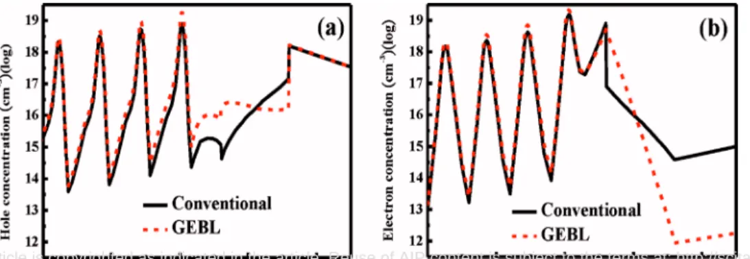
The profiles of hole and electron concentration distribu-tion at a current density of 100 A/cm2are illustrated in Figs.
3共a兲and 3共b兲, respectively. It can clearly be seen that with GEBL, injected holes uniformly distribute along the EBL region compared to conventional one, demonstrating that the flat valence band indeed favored the hole transportation across EBL. Meanwhile, the hole concentration in MQWs is significantly increased as expected. Moreover, the electron concentration in MQWs is also enhanced, while the electron distribution within the GEBL region and p-GaN is enor-mously decreased over two orders. This result indicates that GEBL can suppress the electron overflow out of active re-gion more effectively than conventional EBL, even though the conduction band offset between the last GaN barrier and the GEBL is diminished.
Then, the LED structures with EBL and GEBL were grown on c-plane sapphire substrates by MOCVD. After de-positing a low temperature GaN nucleation layer, a 4 m n-type GaN layer, and a ten-pair InGaN/GaN superlattice prestrain layer, the rest of the LED structures were grown based on our simulation design. The epitaxial recipe for the GEBL is worth noting. Generally, the graded-composition ternary III-nitride semiconductors can be grown by two methods: growth temperature ramping and III/III ratio ramping.12,13 Here we adopted the Al/Ga ratio ramping be-cause the temperature ramping would change the growth rate, and the higher temperature might damage the quality of QWs. The growth temperature of conventional EBL and GEBL was the same 共870 °C兲, and the aluminum-composition profile of the GEBL was approximately graded from 0% to 25%. Finally, the LED chips were fabricated by regular chip process with ITO current spreading layer and Ni/Au contact metal, and the size of mesa is 300 ⫻300 m2. The emission wavelengths of both LEDs were around 450 nm at 22 A/cm2.
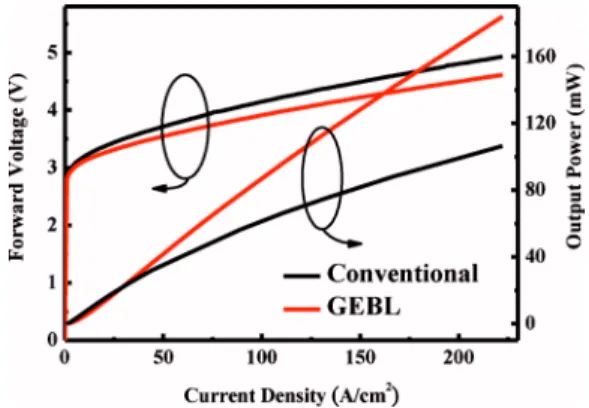
Figure4shows the L-I-V curves of the conventional and GEBL LEDs. The output powers were measured with a cali-brated integrating sphere. The forward voltages 共Vf兲 at
22 A/cm2 and series resistances 共Rs兲 of GEBL LED are
3.28 V and 7 ⍀, respectively, which are lower than that of 3.4 V and 8 ⍀ for conventional LED. The reduced Vfand Rs
can be attributed to the improvement in hole injection and the higher-efficiency p-type doping in GEBL.14In the case of FIG. 2. 共Color online兲 Calculated energy band diagrams of 共a兲 Al0GaN to
Al0.15Ga0.85N,共b兲 Al0GaN to Al0.25Ga0.75N, and共c兲 Al0GaN to Al0.35Ga0.65N graded-composition EBLs at a current density of 100 A/cm2.
FIG. 3. 共Color online兲 Calculated 共a兲 hole concentration distribution and共b兲 electron concentration distribution of conventional and GEBL LEDs at a current density of 100 A/cm2.
261103-2 Wang et al. Appl. Phys. Lett. 97, 261103共2010兲
This article is copyrighted as indicated in the article. Reuse of AIP content is subject to the terms at: http://scitation.aip.org/termsconditions. Downloaded to IP: 140.113.38.11 On: Wed, 30 Apr 2014 09:51:52
L-I curves in Fig. 4, although the output power of GEBL LED is a little lower at low current density 共below 30 A/cm2兲, it increases more rapidly as the injection current
increases as compared to the conventional one. The output powers were enhanced by 40% and 69% at 100 and 200 A/cm2, respectively. This phenomenon can be ex-plained as follows: at low current density, it is more difficult for holes to tunnel across the barrier at the interface of p-GaN and EBL in GEBL LED because the ⌬Ev is larger
than that in conventional LED. While at high current density, the tunneling process of holes can be negligible, and the diffusion process is dominated for the hole transportation into the MQW.5As discussed above, the diffusion process in GEBL is much easier than that in conventional one due to the flat valence band and much lower⌬Evat the interface of the last GaN barrier and EBL. In conjunction with the superior electron confinement, much stronger light output was achieved in GEBL LED at high current density.
Finally, the normalized efficiency of conventional and GEBL LEDs as a function of current density was investi-gated, as shown in Fig.5. The maximum efficiency共peak兲 of
GEBL LED appears at an injection current density of 80 A/cm2, which was much higher than that for
conven-tional LED共at 20 A/cm2兲. More interestingly, the efficiency
droop, defined as 共peak−200 A cm−2兲/peak, was reduced from 34% in conventional LED to only 4% in GEBL LED. This significant improvement in efficiency can be mainly attributed to the enhancement of hole injection as well as electron confinement, especially at high current density.
In conclusion, we have designed a graded-composition electron blocking layer for InGaN/GaN LED by employing the band-engineering. The simulation results showed that the triangular barrier of conventional EBL at the valence band could be balanced, while the slope of the conduction band could be increased by increasing the band-gap of AlxGa1−xN along the关0001兴 direction. As a result, the hole concentration in MQWs was significantly increased, while the electron dis-tribution within the GEBL region and p-GaN was enor-mously decreased over two orders, indicating that the GEBL can effectively improve the capability of hole transportation across the EBL as well as the electron confinement. Further-more, the LED structure with GEBL was realized by MOCVD. The L-I-V characteristics of GEBL LED showed the smaller Vf and Rsdue to the improvement in hole
injec-tion and the higher-efficiency p-type doping in GEBL as compared to the conventional LED. More importantly, the efficiency droop was reduced from 34% in conventional LED to only 4% in GEBL LED. This work implies that carrier transportation behavior could be appropriately modi-fied by employing the concept of band-engineering.
The authors would like to thank Dr. T. C. Hsu and Dr. M. H. Shieh of Epistar Corporation for their technical support. This work was funded by the National Science Council of Taiwan under Grant No. NSC 98-3114-M-009-001 and NSC 98-3114-E-009-002–CC2.
1U.S. Department of Energy,http://www.energy.gov/.
2M.-H. Kim, M. F. Schubert, Q. Dai, J. K. Kim, E. Fred Schubert, J. Piprek, and Y. Park,Appl. Phys. Lett. 91, 183507共2007兲.
3C. H. Wang, J. R. Chen, C. H. Chiu, H. C. Kuo, Y. L. Li, T. C. Lu, and S. C. Wang,IEEE Photonics Technol. Lett. 22, 236共2010兲.
4A. David, M. J. Grundmann, J. F. Kaeding, N. F. Gardner, T. G. Mihopou-los, and M. R. Krames,Appl. Phys. Lett. 92, 053502共2008兲.
5S.-H. Han, D.-Y. Lee, S.-J. Lee, C.-Y. Cho, M.-K. Kwon, S. P. Lee, D. Y. Noh, D.-J. Kim, Y. C. Kim, and S.-J. Park,Appl. Phys. Lett. 94, 231123 共2009兲.
6S. Choi, H. J. Kim, S.-S. Kim, J. Liu, J. Kim, J.-H. Ryou, R. D. Dupuis, A. M. Fischer, and F. A. Ponce,Appl. Phys. Lett. 96, 221105共2010兲. 7Y. K. Kuo, M. C. Tsai, and S. H. Yen,Opt. Commun. 282, 4252共2009兲. 8S. C. Ling, T. C. Lu, S. P. Chang, J. R. Chen, H. C. Kuo, and S. C. Wang,
Appl. Phys. Lett. 96, 231101共2010兲.
9J. Piprek, Nitride Semiconductor Devices: Principles and Simulation 共Wiley-VCH, Berlin, 2007兲, p. 279.
10I. Vurgaftman and J. R. Meyer,J. Appl. Phys. 94, 3675共2003兲. 11M. Katsuragawa, S. Sota, M. Komori, C. Anbe, T. Takeuchi, H. Sakai, H.
Amano, and I. Akasaki, J. Cryst. Growth 189–190, 528共1991兲. 12C. K. Sun, T. L. Chiu, S. Keller, G. Wang, M. S. Minsky, S. P. DenBaars,
and J. E. Bowers,Appl. Phys. Lett. 71, 425共1997兲.
13M.-H. Kim, Y.-G. Do, H. C. Kang, D. Y. Noh, and S.-J. Park,Appl. Phys. Lett. 79, 2713共2001兲.
14J. Simon, V. Protasenko, C. Lian, H. Xing, and D. Jena,Science 327, 60 共2010兲.
FIG. 4. 共Color online兲 Forward voltage and output power as a function of current density for conventional and GEBL LEDs.
FIG. 5.共Color online兲 Normalized efficiency as a function of current density for conventional and GEBL LEDs.
261103-3 Wang et al. Appl. Phys. Lett. 97, 261103共2010兲
This article is copyrighted as indicated in the article. Reuse of AIP content is subject to the terms at: http://scitation.aip.org/termsconditions. Downloaded to IP: 140.113.38.11 On: Wed, 30 Apr 2014 09:51:52