Abstract—Several types of poly-Si nanowire (NW) thin-film
transistors (TFTs) with multiple-gated (MG) configuration were demonstrated and characterized. These devices were fabricated with simple methods without resorting to costly lithographic tools and processes. The fabricated trigated devices show a low sub-threshold swing (SS) of around 100 mV/dec and on/off current ra-tio higher than 108. These results clearly indicate the effectiveness of MG scheme in enhancing the device performance. Furthermore, a multiple-channel scheme was demonstrated to further increase the drive current without compromising device performance. Fi-nally, the impact of MG on the variation of NWTFT characteris-tics is investigated with a clever method that allows the fabrication of test structures with identical NW channel but different gate configurations. The results clearly show that the variation could be reduced by increasing the portion of NW channel surface that is modulated by the gate.
Index Terms—Field-effect transistor, multiple-gate (MG),
nano-wire (NW), poly-Si, variation.
I. INTRODUCTION
T
HE FINE-GRAIN structure of poly-Si thin-film transis-tors (poly-Si TFTs) is known to affect the carrier transport and device performance. Various methods have been proposed to enlarge the grain size of poly-Si thin films, including excimer laser annealing [1] and metal-induced lateral crystallization [2], in order to improve device characteristics. An alternative ap-proach to minimize the negative impacts of the granular struc-ture of the poly-Si film is to reduce the total amount of defects by thinning down the channel body. Recently, we have proposed a simple method to fabricate poly-Si nanowire (NW) TFTs by using sidewall spacer etching technique to define poly-Si NW channels, and the fabricated devices feature a single side-gate structure [3]. Improved characteristics over the planar counter-parts, including reduced short channel effects and steepersub-Manuscript received May 22, 2008; revised July 22, 2008. Current version published October 30, 2008. This work was supported in part by the National Science Council of the Republic of China under Contract NSC 96-2221-E-009-212-MY3. The review of this paper was arranged by Editor G. Cohen.
H.-H. Hsu, T.-W. Liu, L. Chan, and T.-Y. Huang are with the Institute of Electronics, National Chiao Tung University, Hsinchu 300, Taiwan, R.O.C.
C.-D. Lin is with the National Nano Device Laboratories, Hsinchu 300, Taiwan, R.O.C.
H.-C. Lin is with the Institute of Electronics, National Chiao Tung Univer-sity, Hsinchu 300, Taiwan, R.O.C., and also with the National Nano Device Laboratories, Hsinchu 300, Taiwan, R.O.C. (e-mail: hclin@faculty. nctu.edu.tw).
Color versions of one or more of the figures in this paper are available online at http://ieeexplore.ieee.org.
Digital Object Identifier 10.1109/TED.2008.2005161
threshold swing (SS), have been achieved [4]. However, the on current of the proposed NW devices is limited by the small con-duction width inherent with the single side-gate structure. This limitation is undesirable for practical applications. Moreover, for most NW fabrication methods, the poor controllability over NW diameter and uniformity would lead to large variations of device characteristics such as threshold voltage, on current, and SS [5], [6]. These issues must be carefully addressed before the NW devices can be inducted to practical application and mass production. In line with this, the adoption of a multiple-gated (MG) structure is promising [7], [8]. The MG configuration is expected to further improve the performance of poly-Si NWTFT devices through an increase in the effective channel width and enhanced gate controllability over the channel. In this paper, we propose new and simple methods for fabricating MG poly-Si NW devices without resorting to advanced lithographic tools. The fabrication of the MG poly-Si TFTs is described in the next section. The proposed device structures include trigate configuration. Fundamental characteristics of such trigate devices are presented and discussed in Section III. To investigate the effectiveness of MG configurations, we also propose a clever scheme (described in Section II) to fabricate devices with identical NW channels but different gate configurations. Then, fluctuation properties of these fabricated devices are investigated and discussed in Section IV. Impacts of MG configurations on the variation of device performance could be unambiguously clarified with the designed test structures. In the final section, a brief summary is given.
II. DEVICESTRUCTURES ANDFABRICATION
Fig. 1(a) and (b) shows top (layout) and cross-sectional views [along the A–B direction in Fig. 1(a)], respectively, of the proposed trigated poly-Si NWTFT. It can be seen that three out of the four sides of the NW channels are modulated by the gate to ensure good gate controllability. Fig. 2 shows the schematic process flow. The fabrication began on Si wafers capped with a 100-nm-thick thermal oxide. Next, a 40-nm-thick TEOS oxide and a 50-nm-thick nitride were deposited by low-pressure chemical vapor deposition to serve as sacrificial and hard-mask layers, respectively [Fig. 2(a)]. After definition and formation of a dummy gate, the TEOS oxide was shrunk by a selective etching performed in an HF-containing solution, so as to form cavities underneath the nitride hard mask [Fig. 2(b)]. Then, a 100-nm-thick conformal amorphous-Si layer was deposited,
Fig. 2. Schematic process flow for the trigated NWTFT.
Fig. 3. Cross-sectional TEM images of a trigated NW device.
Fig. 4. Key steps for fabricating NWTFTs with various gate configurations.
Fig. 5. TEM pictures of (a) S2 and (b) S3 NWTFTs.
followed by an annealing step performed at 600 ◦C in N2 ambient for 24 h to transform the amorphous-Si into poly-Si. Source/drain (S/D) doping was then performed with phospho-rus ion implantation [Fig. 2(c)]. After the generation of S/D photoresist p atterns with a lithographic step, a reactive plasma etching step was performed. Owing to the anisotropic etching process, poly-Si NW channels underneath the nitride hard mask were formed simultaneously during the S/D etching step
Fig. 6. (a) Transfer and output characteristics of trigated NWTFT with (b) L = 0.4 μm and (c) L = 5 μm.
Fig. 7. Layout of an NWTFT with multiple-channel (number of chan-nels is 18).
Fig. 8. Transfer characteristics of trigated NWTFT with various NW channel number.
Fig. 9. Normalized drain–current (to a single-channel device) and SS of NWTFTs as a function of channel number.
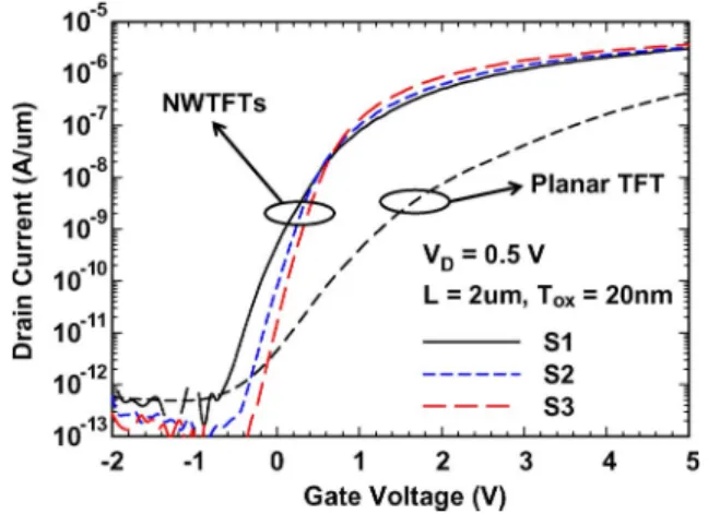
Fig. 10. Transfer characteristics of S1, S2, and S3 NWTFTs with L = 2 μm.
[Fig. 2(d)]. Subsequently, the sacrificial nitride and TEOS oxide layers were selectively removed by a two-step wet-etching process [Fig. 2(e)] to expose the poly-Si NW, and a 20-nm-thick TEOS oxide layer was deposited to serve as the gate dielectric. Then, a 100-nm-thick in situ doped n+ poly-Si was deposited and patterned to serve as the gate electrode [Fig. 2(f)]. All devices were then covered with a 200-nm-thick TEOS oxide passivation layer. Finally, after the formation of test pads using standard metallization steps, all fabricated devices received a NH3plasma treatment for 2 h.
Fig. 12. Mean and standard deviation of threshold voltage (VTH) of NWTFTs with (a) L = 0.7 μm and (b) L = 5 μm. For each device condition, 20 samples
were characterized.
Note that the etching rate of TEOS oxide in the shrinkage step was adjusted to a low value but with high selectivity to both nitride hard mask and underlying thermal oxide layers. As a result, the cross-sectional dimensions of poly-Si NW channel can be easily reduced to sub-100-nm scale with a careful control of the etching time. Cross-sectional TEM images of a device with an NW channel as thin as 8 nm wrapped by the trigate are shown in Fig. 3.
A clever scheme for the fabrication of NW devices with identical NW channels but various gate configurations was also developed. Key steps of the device fabrication are shown in Fig. 4. First, TEOS and nitride were formed on Si substrates capped with buried oxide [Fig. 4(a)]. After the patterning of the top nitride layer with an anisotropic plasma etching step, an isotropic wet-etching process was used to etch the TEOS oxide layer and form cavities under the SiN layer, as shown in Fig. 4(b). The following process steps before the removal of hard mask [Fig. 4(b) and (d-1)] were basically similar to those shown in Fig. 2(c). Next is the key step to determine the gate configuration: For Structure 1 (S1), the nitride hard mask and dummy TEOS were retained [Fig. 4(d-1)] by skipping the etching process. For Structure 2 (S2), the nitride hard mask was selectively removed with a wet etching [Fig. 4(d-2)], and the dummy TEOS was retained. For Structure 3 (S3) which has a gate-all-around (GAA) configuration, both nitride hard mask and dummy TEOS were removed [Fig. 4(d-3)]. Subsequently, a 20-nm-thick TEOS gate oxide and an n+poly-Si gate were
Fig. 13. Standard deviations of VTHas a function of (LW )−1/2for both
planar and NWTFTs.
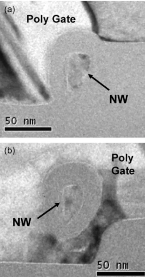
formed in all devices [Fig. 4(e-1)–(e-3)]. All fabricated de-vices then received NH3 plasma treatment for 2 h. The three structures which have NW channels of identical shape and size would allow us to investigate and clarify the impacts of MG configurations on device performance as well as the variation of device characteristics. TEM pictures of S2 and S3 NW devices are shown in Fig. 5(a) and (b), respectively. The NWs of the two devices exhibit identical cross-sectional shape with total peripheral length of around 110 nm, confirming our postulation stated earlier.
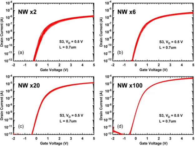
Fig. 14. Transfer characteristics of NWTFTs with S3 structure for channel number of (a) 2, (b) 6, (c) 50, and (d) 100. The channel length is 0.7 μm. In each figure, 20 samples were characterized.
III. ELECTRICALCHARACTERISTICS OFTRIGATEDPOLY-SITFTs
Fig. 6 shows the transfer and output characteristics of trigated NWTFTs with channel length of 0.4 and 5 μm, respectively. It should be noted that a very steep SS as low as 100 mV/dec (at
VD= 3 V) is achieved, owing to the excellent controllability
of trigate over the ultrathin NW channels. For the device with 0.4-μm channel length, excellent on/off current ratio up to 4.5× 10⁸is obtained, while the drain-induced barrier lowering is negligible, despite the rather thick gate oxide (20 nm). To fur-ther effectively increase the drive current, devices with multiple NW channels were also fabricated and characterized. Fig. 7 shows an example of such multiple-channel layout with 18 NW channels. Transfer characteristics of trigated NWTFTs, with channel number of 18, 50, and 100, are shown and compared in Fig. 8. On/off-current ratio larger than 108 is obtained for devices with a large number of channels. The on current is extracted at VG− VTH= 3 V and VD= 3 V. Fig. 9 shows
the extracted SS and on current of multiple-channel NWTFTs normalized to a single-channel device as a function of NW channel number. It can be seen that the on current is simply proportional to the number of NW channels, while the SS of the devices are all around 100 mV/dec.
IV. VARIATIONS OFNWTFT CHARACTERISTICS
Variations of the device characteristics are characterized with the three types of NW devices shown in Fig. 4. Fig. 10 shows
typical transfer characteristics of NWTFTs with different gate configurations. For comparisons, data measured from a planar device with poly-Si channel of 50 nm and gate oxide and channel length identical to the NW devices are also included in the figure. The drain–current is normalized to the channel width. From the figure, it is clearly seen that the NW devices show improved performance in terms of steeper SS, lower off current, and higher drive current as compared with the planar one. The improvements are attributed to the reduction in the amount of defects contained in the channels with the NW structure. Among the three NW devices, S3 device exhibits the best performance, owing to its enhanced gate controllability with the GAA configuration.
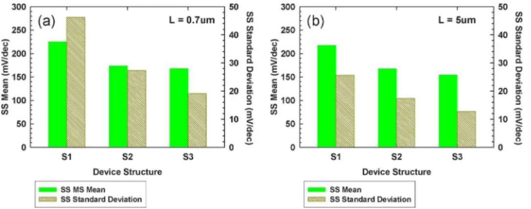
The mean value and standard deviation of SS for de-vices of different gate configurations with channel length of 0.7 and 5 μm are shown in Fig. 11(a) and (b), respectively. In the figures, we can see that long-channel (5 μm) devices have smaller SS deviation than the short-channel (0.7 μm) counterparts. Furthermore, S3 (GAA) structure has the smallest variation among the three gate configurations. Similar trend can also be found in threshold-voltage (VTH) distribution, as shown in Fig. 12 (in this paper, VTH is defined as VG at ID= W/L× 10 nA).
The earlier findings are consistent with the observations reported in the literature that the variation of device characteris-tics increases as the device shrinks [9]. For bulk CMOS devices, major fluctuation sources include doping concentration in the channel, thickness uniformity of thin films, S/D resistance, and
of NW cross section is negligible. Fig. 13 shows the standard deviations of VTH as a function of (LW)−1/2 (the “Pelgrom plot” [12]) with different types of gate structure, and the exper-imental data are consistent with the model. For comparisons, the results obtained from planar TFT devices with identical gate oxide thickness are also included in the figure. Note that the effective channel width of one NW channel in S1, S2, and S3 structures are 40, 65, and 110 nm, respectively (Fig. 5). It is seen that the slope of linear-regression lines for the NW splits are lower than that of conventional planar TFTs. This is mainly attributed to the tiny body of NW channels which leads to a much thinner Wdthan that of planar devices. It should also be
noted that the slope of the regression line for S3 structure is the lowest among the three splits of NWTFTs. This is a clear indication of the effectiveness of trigate structure in reducing the impact of substrate depletion layer.
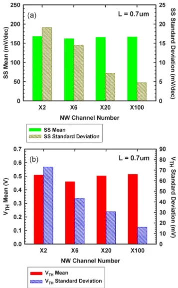
Further reduction in the variation of device characteristics is expected with the use of multiple-channel layout shown in Fig. 7, owing to the increase in the total conduction width. This is shown in Fig. 14, in which the transfer characteristics of devices with channel number of 2, 6, 20, or 100 are shown. In each figure, 20 devices were measured. We can clearly see that the distribution of the measured I–V characteristics become tighter as the channel number increases. The mean value and standard deviations of VT H and SS for
multiple-channel devices built with S3 structure are shown in Fig. 15(a) and (b), respectively. As channel number increases, deviations of VT Hand SS both indeed become smaller.
V. CONCLUSION
In this paper, we have investigated the effects of MG con-figuration on the characteristics of poly-Si NWTFTs. A novel trigate poly-Si NWTFT that can be fabricated without resorting to advanced lithographic tools is proposed. The fabricated de-vices exhibit excellent on/off-current ratio higher than 108and steep SS as low as 100 mV/dec. Moreover, a multiple-channel layout scheme is also proposed and demonstrated to multiply the drive current without degrading device performance. In addition, we have also proposed a clever scheme to fabricate three types of poly-Si NWTFTs with different gate configu-rations but identical NW channels. Such scheme allows us to investigate the impact of MG configuration on the performance variation of poly-Si NW devices. Our results clearly indicate that the S3 structure, which has the largest portion of the NW
Fig. 15. Mean value and standard deviation of (a) SS and (b) VTHfor S3
devices of various channel number.
channel surface under effective gate modulation, shows the least fluctuation in SS and threshold voltage. Additionally, with the increase in channel number of the NWTFT, the device fluctuation can be further suppressed.
ACKNOWLEDGMENT
The authors would like to thank the National Nano Device Laboratories for the assistance in device fabrication.
REFERENCES
[1] G. K. Giust and T. W. Sigmon, “High-performance thin-film transistors fabricated using excimer laser processing and grain engineering,” IEEE
Trans. Electron Devices, vol. 45, no. 4, pp. 925–932, Apr. 1998.
[2] S. W. Lee, T. H. Ihn, and S. K. Joo, “Fabrication of high-mobility p-channel poly-Si thin film transistors by self-aligned metal-induced lateral crystallization,” IEEE Electron Device Lett., vol. 17, no. 8, pp. 407–409, Apr. 1996.
[3] H. C. Lin, M. H. Lee, C. J. Su, T. Y. Huang, C. C. Lee, and Y. S. Yang, “A simple and low-cost method to fabricate TFTs with poly-Si nanowire channel,” IEEE Electron Device Lett., vol. 26, no. 9, pp. 643–645, Sep. 2005.
[4] H. C. Lin, M. H. Lee, C. J. Su, and S. W. Shen, “Fabrication and char-acterization of nanowire transistors with solid-phase crystallized poly-Si channels,” IEEE Trans. Electron Devices, vol. 53, no. 10, pp. 2471–2477, Oct. 2006.
[8] D. Hisamoto, W. Lee, J. Kedzierski, E. Anderson, H. Takeuchi, K. Asana, T. King, J. Bokor, and C. Hu, “A folded-channel MOSFET for deep-sub-tenth micron era,” in IEDM Tech. Dig., 1998, pp. 1032–1034.
[9] A. Asenov, A. R. Brown, J. H. Davies, S. Kaya, and G. Slavcheva, “Simulation of intrinsic parameter fluctuations in decananometer and nanometer-scale MOSFETs,” IEEE Trans. Electron Devices, vol. 50, no. 9, pp. 1837–1852, Sep. 2003.
[10] G. Roy, A. R. Brown, F. Adamu-Lema, S. Roy, and A. Asenov, “Sim-ulation study of individual and combined sources of intrinsic param-eter fluctuations in conventional nano-MOSFETs,” IEEE Trans. Electron
Devices, vol. 53, no. 12, pp. 3063–3070, Dec. 2006.
[11] K. Takeuchi, T. Tatsumi, and A. Furukawa, “Channel engineering for the reduction of random-dopant-placement-induced threshold voltage fluctuation,” in IEDM Tech. Dig., 1997, pp. 841–844.
[12] M. J. M. Pelgrom, A. C. J. Duinmaijer, and A. P. G. Welbers, “Matching properties of MOS transistors,” IEEE J. Solid-State Circuits, vol. 24, no. 5, pp. 1433–1439, Oct. 1989.
Hsing-Hui Hsu was born in Taipei, Taiwan, R.O.C.,
in 1982. He received the B.S. degree in electrical engineering from the National Taiwan University, Taipei, in 2004 and the M.S. degree from the Insti-tute of Electronics, National Chiao Tung University, Hsinchu, Taiwan, in 2008, where he is currently working toward the Ph.D. degree in the Institute of Electronics.
His current research interests include the fabrica-tion and characterizafabrica-tion of Si nanowire FETs and memory devices.
Ta-Wei Liu was born in Changhua, Taiwan, R.O.C.
He received the B.S. and M.S. degrees in ma-terials science and engineering from the Institute of Electronics Engineering, National Chiao Tung University, Hsinchu, Taiwan, in 2006 and 2008, respectively.
His research interests focus on the NW-TFTs fab-rication and characteristic fluctuation.
Chuan-Ding Lin was born in Hsinchu, Taiwan,
R.O.C., in 1970. He was graduated from Ming-Hsin Institute of Technology, Hsinchu, in 1992.
He is currently an Engineer with the National Nano Device Laboratory, Hsinchu, where he is responsible for process integration and develop-ment. His main research interests include dry-etching processing and novel nanodevice-fabrication devel-opment. He has coauthored several technical papers in international conferences.
Tiao-Yuan Huang (S’78–M’78–SM’88–F’95)
re-ceived the B.S.E.E. and M.S.E.E. degrees from the National Cheng Kung University, Tainan, Taiwan, R.O.C., in 1971 and 1973, respectively, and the Ph.D. degree from the University of New Mexico, Albuquerque, in 1981.
In 1977, he left for the U.S. for his Ph.D. studies after serving two years in the Taiwanese navy as fulfillment of his conscription duty. He has worked in the U.S. semiconductor industry for 14 years prior to his return to his native country, Taiwan. Since 1995, he has been a Professor with the Institute of Electronics, National Chiao Tung University, Hsinchu, Taiwan.
Dr. Huang was the recipient of the Semiconductor International’s Technology Achievement Award for his invention and demonstration of the fully overlapped lightly doped drain MOS transistors.
Horng-Chih Lin (S’91–M’95–SM’01) was born
in I-Lan, Taiwan, R.O.C., on August 1, 1967. He received the B.S. degree from the Department of Physics, National Central University, Chung-Li, Taiwan, in 1989 and the Ph.D. degree from the Insti-tute of Electronics, National Chiao Tung University (NCTU), Hsinchu, Taiwan, in 1994.
From 1994 to 2004, he was with the National Nano Device Laboratories, where he was engaged in the research projects of nanoscale-device technol-ogy development. In 2004, he joined the faculty of NCTU, where he is currently a Professor with the Institute of Electronics. Currently he is also a joint-appointment researcher with the National Nano Device Laboratories. His current research interests include thin-film transistor fabrication and characterization, reliability of CMOS devices, and nanowire device technology. He has authored or coauthored over 100 technical papers in international journals and conferences in the these areas.
Dr. Lin served on the program committee of the International Reliability Physics Symposium in 2001 and 2002, respectively, and the International Conference on Solid State Devices and Materials from 2005 to 2008.