The proliferation of chemical mechanical polish (CMP) pla-narization in recent years has not been accompanied by an adequate level of knowledge of the fundamental mechanisms involved. Such a poor understanding inevitably leads to difficulties and often confu-sion when it comes to process control. Among the critical manufac-turing issues, one of the challenges is to manage the within wafer nonuniformity (WIWNU). Mitigation of WIWNU through the adjust-ment of machine parameters, such as pad speed and down force, has been reported previously.1,2However, little has been revealed regard-ing the root cause of WIWNU, and a systematic methodology for controlling it does not yet exist. While it is generally agreed that pres-sure distribution and variation in relative velocity are the two main factors influencing WIWNU, how these two factors may vary in the presence of the rotating pad and carrier, the flowing slurry, and the wafer itself still remains obscure and deserves further investigation.
A further complication arises when the shape, e.g., the curvature of the wafer is considered. Under the presence of down force and back-side pressure, the wafer curvature (characteristics of film stress) may induce uneven stress distribution along the direction nor-mal to wafer, and irregular slurry flow on the plane of the wafer, both of which may contribute to WIWNU. Previous experimental results indicated that the magnitude of prepolish film stress (or wafer bow) affected both the removal rate and WIWNU. It was found in one study that the mean removal rate decreases while the WIWNU increases as the compressively stressed thermal oxide on one side of Si substrate (i.e., convex wafer shape) was thinned down by the con-tinuous polish process (i.e., decreasing wafer bow).3Conversely, in another study,4both the removal rate and WIWNU were found to decrease with increasing prepolish wafer bow, from negative (con-cave, tensile stress) to positive (convex, compressive stress). Neither of the two studies above has given a proper physical model to account for the observed wafer curvature effects on the CMP process, although both speculated that the existence of the wafer bow makes it difficult to flatten the wafer when the carrier was pressed against it, giving rise to polish nonuniformity.
In this contribution, we examine the wafer curvature (film stress) effects on removal rate and WIWNU both theoretically and experi-mentally. A model based on Hertzian contact stress is proposed to simulate the wafer-scale pressure distribution, given carrier configu-ration, down force, back pressure, pad stiffness, and wafer curvature. In conjunction with a proper removal rate model, this calculated pressure profile can then be converted into theoretical WIWNU. Experiments with thermal and plasma-enhanced chemical vapor deposited (PECVD) oxides on the Si wafer with controlled stress level were performed to verify the validity of the proposed model.
The general effects of film stress upon removal rate and WIWNU are discussed.
Model Construction
Curvature-induced wafer-scale pressure distribution.—There are
many sources that can lead to wafer bow and deflection during inte-grated circuit (IC) manufacturing. In the current study, we consider only the defection due to the existence of intrinsic and thermal film stresses. These stresses may be tensile (negative bow) or compres-sive (positive bow), depending on the deposition process and thermal history. First, the wafer is considered as a thin circular plate while the pad is regarded as a half space. The wafer/pad contact area is approximated as a bowl with radius a defined in Fig. 1. The applied down force exerts an axially symmetric uniform pressure profile onto the wafer. In order to simplify the case, the effect of slurry flow is neglected and the interaction between wafer and pad is assumed frictionless. In other words, this is the contact problem that obeys the conditions required by Hertizan contact theory.
Since the wafer is axially symmetric, all variables are constructed in the radial coordinate. In this case, the total pressure on the wafer surface can be expressed as the sum of separate pressure components
Psum5 Puniform1 DP(Pcontact) [1] where Puniform is the wafer pressure arising from uniform down force, Pcontactis the pressure intensity due to wafer contact, and
Psumis the sum of these pressures.
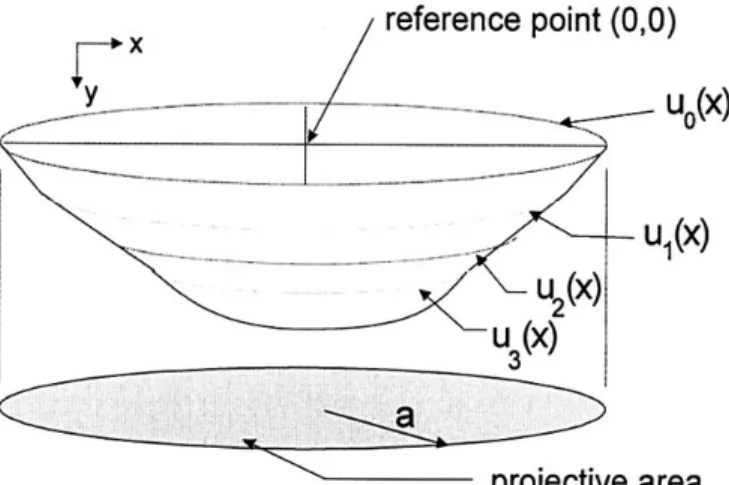
From Green’s function for contact problem,5we can obtain the normal displacement uy(x) at the point (x, 0) on the contact region as shown in Fig. 2 [2] u x G A p x d 0 w 1 ( )5 2 1k ( ) logj 2 j j p 4
∫
Effects of Film Stress on the Chemical Mechanical Polishing Process
Wei-Tsu Tseng,
a,* Yiao-Hsien Wang,
band Jyh-Hwa Chin
baDepartment of Materials Science and Engineering, National Cheng-Kung Univeristy, Tainan 701, Taiwan bDepartment of Mechanical Engineering, National Chiao-Tung University, Hsinchu 300, Taiwan
A theoretical model is constructed to simulate the pressure distribution arising from wafer curvature (film stress) during chemical mechanical polishing (CMP), based on theories of elastic contact stress. Results from oxide CMP experiments suggest that the wafer curvature results in a nonuniform polish rate distribution across the wafer, in agreement with the simulation based on the model. This stress-dependent polish nonuniformity is attributed to the nonuniform pressure distribution across the wafer, induced by the wafer radius of curvature (film stress). Also, it was found that the magnitude of oxide film stress itself has little effect on removal rate. Oxides with tensile stress tend to have a weakened bond structure and enhanced chemical reactivity, both of which result in slightly higher removal rates. The reverse is true for oxides with compressive stress. Deviations from the model predic-tion may result from the stress induced by slurry flow, local variapredic-tions in wafer shape and form, and pad surface properties. © 1999 The Electrochemical Society. S0013-4651(99)03-063-3. All rights reserved.
Manuscript submitted March 16, 1999; revised manuscript received July 1, 1999. This was in part Paper 1116 presented at the San Diego, California, Meeting the Society, May 5-7, 1998.
S0013-4651(99)03-063-3 CCC: $7.00 © The Electrochemical Society, Inc.
where x represents the position located on the contact region in hor-izontal direction,k is plane stress ratio, u0(x) is a function of x which describes the deflection at point (x, 0), uy(x) is a function of x describing the deflection at point (x, y).
Substituting Eq. 2 into Cauchy singular integral equation for unknown pressure p(j) yields the following expression
[3] The geometric relations of the contact area as shown in Fig. 3a and b require that
2 5 2 1 j j 2 j 2 2 du dx G p d x a x a a a 0 w 1) (k ( ) p 4
∫
< < x5 a cos w j 5 a cos u [4]where x is the horizontal distance between center and point C (O1
—
D —
), w is the angle between O1
——
C and O1
—
D —
,j is the horizontal distance between center and point E (O1
—
F —
), and u 5 the angle between (O2
— E — ) and (O2 — F —
) . Expanding both sides of Eq. 4 as a Fourier series, and substituting them into Eq. 3
[5]
Using the formula proposed by Muskhelihvili6
[6]
[7]
one can find
[8]
and hence
[9]
Also, the pressure, distribution p(j), can be equated to the force F by the following
[10]
Now, assume that the load F is sufficient to establish contact over the entire contact area, then the displacement of the half-plane must satisfy the condition
uy(x) 5 2u0(x) 1 C1x1 C0 [11]
Let the curvature of the wafer be Rc, then the displacement is cor-related with Rcand x by the following equations
[12]
[13] Since the wafer is axially symmetric, u0(x) 5 u0(2x), the results in C15 0.
From Eq. 7 and 13, for a wafer with concave curvature, we have [14] [15] p G a R 2 2 5 1 w c(k 1) u a R 2 5 2 c 2 u x C C x x R C a R a R 0 2 4 4 ( )5 0 1 1 1 5 2 cos 2 2 c 0 2 c 2 c 2 ⋅ w d u dx R 2 0 2 c 1 5 2 5 2 5 5 ~ a p n d ap n n 0 0
∑ ∫
p u u p cos 0 F p d p d p a d A a a 5 2 5 2 5 2 2∫
( )j j∫
( )j j∫
0 ( )u u u p sin p G u a n n5 n 1 4 1 1 w k(
)
> 5 1 5 ~ ( sin k 1) f w 1 n a G p n n 4∑
n n n u n a G p n 5 5 ~ 5 1 1 4 ∝∑
sin (∑
sin f k f p p f f 1) sin sin w 1 n du d un n 0 w 5 1 w ∝∑
sin p( ) pncosn sin u u u 5 0 ∝∑
1 4 0 0 a du d G p d sin ( ( )sin (cos cos ) w w k p u u u w u w p p 0 w 1) 5 2 1 2∫
< <Figure 2. The perspective of function Uy(x) in wafer pad interface.
Figure 3. (a, top) A schematic showing point C on the contact area. (b,
so that the load is symmetrical to retain equilibrium and hence p15 0. From Eq. 5, 10, and 15, the pressure can be expressed as a func-tion of u
[16] Equation 16 will be singular at u 5 0, p(x 5 6a) unless we choose an a such that
[17]
[18] For plane stress conditions
[19] Substituting Eq. 18 and 19 into Eq. 16
[20]
[21] where F is line load on the wafer. Since F5 2paP,, where P,is the pressure from down force and r> x when Rc>> r, Eq. 20 can be re-expressed as
[22] In a similar fashion, we can solve for the case of wafer with con-vex curvature
[23]
[24] and
[25]
The back pressure Pback-pressureis applied onto the wafer numeri-cally, the pressure intensity due to back pressure is derived from the force equilibrium method in our previous publication.7The overall pressure Psumis the summation of the above, i.e.
Psum5 Puniform1 Pcontact1 Pback pressure [26] Correlation between wafer curvature and film stress.—Thin film
deposition process and postdeposition thermal treatments induce stresses in the film as manifested by the change in wafer curvature. In an ideal case, the film stress is obtained by the Stoney equation8
[27] s5 2n E h R h w w w c f 1 6 2 P p r PR a a R a a a r contact w 2 2 2 2 2 2 5 5 2 2 2 2 ( ) ˜ 2 1 p F a F a ( )u ( u p u p u u 5 2 11cos2 )5 22 2 21 sin sin 1 sin d u dx R 2 0 2 c 5 1 P p r P R a r a p P R a contact w 2 w ) and 4 5 ( 5 24˜⋅ 12 ( )0 52 ˜ ⋅ p x F a x a ( )5 22 2 2 2 2 p p F a F a ( )u ( cos u) p u u p 5 2 12 2 5 2 sin 2 sin 5 21 2nw 1 22nr w p 1 E E k n n k 5 2 2 1 5 3 2 4 w w w com com 1 and ( 1) where 1 G E E a5 F(k1 R pm 1) 2 c F a G a R p 5 k1 2 1) w c( p F a G a R ( ) ( cos sin u p k u u 5 2 1 1 2 1) w c 2
where Ew/12nwis biaxial modulus of the substrate (silicon wafer), hwis substrate thickness, hfis film thickness, Rcis radius of
curva-ture, and s is the film stress. To calculate the change in film stress, the following equation is used
[28]
where Rclis the curvature before film deposition, and Rc2is the
cur-vature after the process. Assuming the wafer is bent symmetrically, the following relationship can be constructed according to the schematic in Fig. 4
2Rw5 RcuAB [29]
[30] where DABis the distance between point A and point B,uABis the angle between —OA— and —OB—, and hg is the gap distance between
wafer and pad.
Since uABis small, Eq. 30 can be reduced to
[31] substituting Eq. 31 into Eq. 29 yields
DAB5 2Rw [32]
the maximum deflection of wafer hgat center is given by
[33] also, from geometry
[34] sinuAB AB 2 2 c 5 D R hg5Rc2RccosuAB 2 D R AB AB 2 5 c u 2 D R AB AB 2 5 c⋅ sin u 2 s5 2n 2 E h h R R w w w f cl c2 1 6 1 2 1
Figure 4. The geometrical relationship of wafer bow. In this case, the wafer
is said to have a downward radius of curvature, manifesting the existence of compressive stress.
S0013-4651(99)03-063-3 CCC: $7.00 © The Electrochemical Society, Inc. then, substitution of Eq. 34 into Eq. 33 results in the expression for
the maximum wafer deflection hg
[35]
since Rc>> hg, Eq. 35 can be rewritten as
[36] Additionally, since DABis small compared with Rc, Dabcan be considered as a constant and then
[37] again from Eq. 34
[38] So, with a given film stress and uAB(e.g., from standard laser scanning technique), the deflection of wafer DABand the gap dis-tance hgcan be determined, and the wafer-scale pressure distribution can be calculated from Eq. 24, 25, and 26.
The pressure profiles calculated based on the model above can be fitted into appropriate polish rate models to determine the theoreti-cal and removal rate and WIWNU. In this study, both Preston’s equation (R.R. 5 KpPV) and Tseng’s model (R.R. 5 MP5/6V1/2, where M is a weighing parameter)9are used to determine the theo-retical removal rates. The latter has been demonstrated experimen-tally to be a more accurate removal rate model for oxide CMP10and is included here for comparison with the Preston equation.
Experimental
Thermal oxides (wet oxides) and PECVD tetraethoxysilane/ ozone (TEOS/O3) oxides were grown/deposited on 150 mm wafers up to a thickness of ,1200 nm. As defined in Fig. 4, stresses in oxide films are carefully tuned to be tensile (upward curvature) or compressive (downward curvature), by varying the deposition con-ditions. CMP experiments were conducted on an IPEC 472 polish system with a “K-groove” pad, R-200 carrier film, and SC-112 slur-ry. The down force and back-side pressure for thermal oxide polish were fixed at 7 and 0 psi, respectively; while those for TEOS/O3 oxides were varied. The platen and carrier rotations are set at 20 and 42 rpm, respectively, for thermal oxides; and 30 and 28 rpm, respec-tively, for TEOS/O3oxides. Ex situ pad dressing was performed at the end of each polish run. These oxide wafers were polished at 1 min intervals up to 7 min. At the end of each min, the wafer curva-ture and stress were measured using the standard laser beam wafer deflection technique. Removal rate and WIWNU (1-s) were meas-ured and calculated at 49 points across each wafer, considering a 4 mm edge exclusion.
Results and Discussion
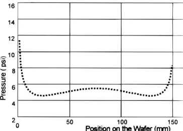
Calculated wafer level pressure distribution.—The pressure
dis-tribution across a wafer under a given down force can be calculated from principles of Hertzian contact stress.5Under a down force of 6 psi, the pressure distribution across a 150 mm wafer in contact with a IC1000/Suba IV composite pad on a IPEC 472 polisher is nonuni-form, with distant edge high characteristics as shown in Fig. 5. In fact, such an across-wafer pressure distribution also correlates well with the removal rate profile along the wafer diameter, as observed in our previous study.7The pressure at wafer center is merely 5.5 psi, while that at the edge may be as high as 12 psi. When the wafer cur-vature (e.g., downward curcur-vature) is considered, the pressure distri-bution is modified, due to the nonuniform elastic response from the
sin 2 AB AB AB AB c c u u 2 5 DR → ≡ D R h R g c ∝ 1 h D R g AB 2 c 8 ≡ h R R D R h R R D g c g c c c 2 c 2 AB 2 AB 2 5 2 12 2 5 2 4 1 2 2 →( )
curved wafer to the applied down force. This can be seen clearly from Fig. 6, which is calculated based on the model proposed in this study. The wafer with a downward curvature is held upside down by the carrier, and a down force of 7 psi is exerted along the center axis of the wafer. The actual pressure experienced by the wafer at its cen-ter is elevated due to the wafer curvature effect.
To provide a better view for this curvature effect, the pressure profiles for wafers with upward and downward curvature are calcu-lated for different radius of curvature, and the results are exhibited in Fig. 7 and 8, respectively. In both cases, the pressures at the wafer edge are larger, in agreement with previous simulation studies.7,11
For wafers with upward curvature (i.e., tensile stress), the pressure is increased across the entire wafer compared with “flat wafers,” such a curvature-induced pressure increase is more pronounced for wafers with larger radius of curvature (lower tensile stress). The situation is slightly different for wafers with downward curvature (compressive stress). In this case, the pressure is also increased and a larger radius of curvature (lower stress) also induces a greater effect. However, the difference in pressure reduces gradually from wafer center to wafer edge, and diminishes eventually at a certain point close to the edge, after which the trend reverses and a shorter downward radius of cur-vature (larger compressive stress) brings about a greater pressure increase. The variation in pressure distribution described above is the root of polish nonuniformity as is discussed later in this paper.
Figure 5. Wafer pressure distribution on a flat 150 mm wafer under a down
force of 6 psi and back pressure of 0 psi. The polisher and pad used are IPEC 472 and K grooved, respectively.
Figure 6. Predicted (calculated) pressure at wafer center in the presence of
Correlation between film stress and removal rate.—Mean
removal rates are plotted against upward and downward wafer cur-vatures of oxide films in Fig. 9 and 10, respectively. The corre-sponding film stress is also shown for comparison. For each curva-ture, three wafers were polished and their removal rates were aver-aged to give a data point on the figures. As shown, for wafers with an upward curvature (tensile stress), the CMP removal rates increase slightly with decreasing radius of curvature (increasing tensile stress). The reverse is true for wafers with a downward radius of cur-vature (compressive stresses).
Cross comparisons between Fig. 7 through 10 suggest that, for oxides with tensile stresses, a smaller film stress (larger radius of curvature) associated with a greater pressure gives rise to a lower (though only marginally) removal rate. Conversely, for wafers with compressive stresses, a smaller stress and thus a greater pressure would result in a higher removal rate. The two behaviors above seem contradictory to one another, since, according to the removal rate models (e.g., Preston’s equation), a greater pressure corresponds to an accelerated wearing rate and hence a higher removal rate.
Haque et al. reported that the existence of a tensile stress com-ponent in the oxide network would make the bonds more reactive and result in a more open structure of the (SiO4)24tetrahedral
net-work in the oxide.12As a consequence, the oxide structure would become more susceptible to the chemical attack by alkaline slurry, leading to a higher removal rate. From another perspective, Nogami and Tomozawa pointed out that the water diffusion rate in silica is a function of local stress.13A local tensile stress in the film leads to an enhanced diffusion coefficient of water of H1in silica. As a conse-quence, the presence of a higher tensile stress in the oxide film would induce a high CMP removal rate through accelerated water/slurry diffusion and the stronger reactivity with the alkaline agent in the slurry. Therefore, the observed removal rate variation can be explained by this stress-assisted chemical erosion effect. For oxides in tension, a lower tensile stress translates to a more moder-ate stress-assisted chemical effect and hence a lower CMP removal rate. Similarly, for oxides in compression, a lower stress would give rise to lower resistance to wearing and chemical erosion, and hence a slower removal rate.
Several previous studies indicated that the CMP removal rate of oxides and nitrides is also a strong function of their bonding config-uration, which is manifested by density and refractive index (RI) in the thin films.14,15In the present study, the measured RI for the ther-mal oxides falls between 1.455 and 1.459, suggesting that the oxides are nearly stoichiometric (IR ,1.46) having virtually the same den-sity. Therefore, we ruled out the effects of density change as the pos-sible cause for the removal rate variation in Fig. 7 to 10.
The fluctuation of mean removal rate in Fig. 9 and 10 may come from multiple sources. First, the mean removal rate is, by its nature, a statistical value averaged over the entire wafer. Nonuniform slurry flow and pad surface condition may have lead to the variation of removal rate. In addition, the model proposed in this study is derived
Figure 7. Across-wafer pressure profile for three different upward radii of
curvature. (Down force 5 6 psi; contact 5 contact stress.)
Figure 8. Across-wafer pressure profile for three different downward radii of
curvature. (Down force 5 6 psi; back-side pressure 5 0 psi.)
Figure 9. Mean removal rates vs. wafer upward radius of curvature for
ther-mal oxide films. The corresponding compressive stress is also included for comparison.
Figure 10. Mean removal rate vs. wafer downward radius of curvature for
thermal oxide films. The corresponding compressive stress is also included for comparison.
S0013-4651(99)03-063-3 CCC: $7.00 © The Electrochemical Society, Inc.
based on the assumption that the wafer is axially symmetric, mean-ing that the curvature (film stress) and wafer shape is uniform. Any deviation (as is usually the case) from this simplification would result in removal rate fluctuation and discrepancy between model prediction and experimental data. Adding to the above complexity is the fact that, in reality, the thin films being polished are deposited over patterned line or hole features distributed across the entire wafer. This would lead to local variations in stress and wafer form, and introduce more fluctuation and scattering in the polish data.
Overall, the results above seem to indicate that the stress-induced bond weakening/strengthening mechanism plays a certain role in the removal process to the extent that it may dominate over the down pressure in determining the removal rate. Still more work is needed to verify this point.
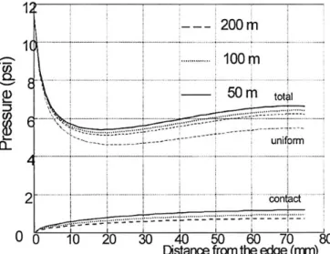
Stress-induced pressure distribution and polish nonuni-formity.—To further clarify the curvature effect, the evolution of
CMP removal rates with the changing wafer curvature were moni-tored at specific locations on a wafer. Figures 11 and 12 show the cen-ter and edge removal rates, respectively, for films with compressive stresses (downward curvature). As polish proceeds, compressive stress (radius of curvature) in the film is relieved (increased), the cen-ter removal rate increases from 810 Å/min at 224 MPa (radius of curvature 5 46 m) to 876 Å/min at 215 MPa (radius of curvature 5 125 m). Meanwhile, the edge removal rate (measured at ,5 mm away from wafer periphery) decreases from 1003 to 943 Å/min cor-respondingly. This would rise to a reduced WIWNU since the differ-ence in polish rate diminishes gradually as polishing progresses. The
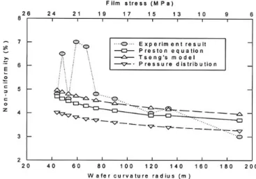
different trends in removal rate at the wafer center and edge are the direct consequence of the curvature-induced pressure profile as shown in Fig. 8. The pressure and WIWNU are expressed in terms of downward wafer radius of curvature in Fig. 13. As can be seen, both the pressure and polish nonuniformity decrease as compressive stress in the film is relieved. In other words, a “flatter” wafer (i.e., smaller stress and larger radius of curvature) would induce a more uniform distribution and thus more uniform material removal during CMP. The correlation between calculated pressure nonuniformity and the experimental WIWNU is distinct. The close agreement between the experimental polish rate and WIWNU and those predicted by the model proposed demonstrates the validity of the model. As polish progresses, the relief in-plane compressive stress due to the thinning of oxide film induces a more uniform distribution of the out-of-plane down pressure across the wafer, leading to a reduced WIWNU. For wafers with upward radius of curvature (tensile stress), the curvature-induced pressure increase should be uniform across the entire wafer as found in Fig. 7. As shown in Fig. 14, and 15, both center and edge removal rates decrease with increasing wafer radius of curvature, in agreement with the prediction. In this case, the curvature effect does not help significantly in reducing the polish nonuniformity since the removal rates at edge and center were increasing concurrently. The WIWNU after the first minute of polish (radius of curvature 5 48 m) is 5.64% (measured) and 4.95 (calculated); while the WIWNU after the last minute of polish (radius of curvature 5 190 m) is 5.38% (measured) and 4.55% (calculated).
Figure 11. Wafer center removal rate vs. downward radius of curvature and
compressive stress for thermal oxide films.
Figure 13. Pressure and polish nonunifomity (WIWNU) as a function of
wafer downward radius of curvature and compressive stress.
Figure 12. Wafer edge removal rate vs. downward radius of curvature for
thermal oxide films.
Figure 14. Wafer center removal rate vs. upward radius of curvature for
Also noted from the figures above (e.g., Fig. 13) is that the theo-retical WIWNU based on the Tseng’s model (standard deviation,s 5 145) is in closer agreement with the experimental results than the one based on the Preston equation (s 5 2.76). This may imply that Tseng’s model is more feasible in predicting the CMP removal rate and its nonuniformity as a function of pressure and velocity. Similar results were also found in our previous studies.9,10
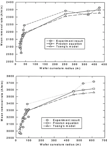
As a further illustration of the model, the effect of back-side pres-sure is also investigated. In this case, PE-TEOS oxides with an ini-tial downward radius of curvature (25 m, stress 5 253 MPa) were polished, and the variation of a 49 point mean removal rate was cal-culated and experimentally measured. The results in Fig. 16 indicate an increasing trend of removal rate with decreasing wafer radius of curvature (compressive stress), similar to the result in Fig. 11 for thermal oxide. When the down force is raised to 11 psi and a back-side pressure of 4 psi is applied, the pressure profile is raised and the removal rates are enhanced. The match between the experiments and theoretical prediction is excellent in both cases.
General remarks.—Several points can be drawn regarding the
stress effects on oxide CMP process based on the results gained in this study. The film stress itself does not contribute significantly to the reduction (compressive stress) or enhancement (tensile stress) of the CMP removal rate. It does, however, induce a redistribution of pressure across the wafer, causing a variation in the mean removal rate and WIWNU. Since the wafer radius of curvature increases as polish progresses, the horizontal axes in Fig. 9 through 15 can be taken as the polish time so that they actually represent the variations of removal rate or nonuniformity with polish time. Such a phenom-enon is frequently encountered in the CMP process, and can now be attributed to the stress (curvature) effect. In addition, the so-called substrate effect,16,17in which the removal rate was found to increase or decrease depending on the substrate material beneath the layer being polished, may actually arise, at least partially, from the curva-ture effect described in the present study.
For metal CMP, the stress effects may become even more compli-cated. Due to their high thermal expansion of coefficient relative to the dielectric substrate, most of the metals, whether W, Al, or Cu, exhibit a tensile stress after deposition. The bond weakening/strengthening mechanism due to stress may also be applicable to metal thin films. However, its net influence on the removal rate may be diluted since an additional plastic deformation energy should be overcome before the metal atom clusters can be broken and polished off. In addition, other attributes, such as grain size18and texture,19may overwhelm this stress effect so that it would be difficult to evaluate the direct impact of stress on the metal CMP removal rate. Finally, the exis-tence of tensile stress in metal films implies that the WIWNU may not decrease with time due to the wafer curvature effect, as in the
case of oxide CMP. Further experimental work is required to verify the speculation above.
Influences from other physical events, such as fluid flow and pad surface feature, in the presence of wafer curvature should be consid-ered in the modeling in order to gain further insight into the origins of polish nonuniformity. Future work for this study would include the variations of down force and back-side pressure in the simulation and experiments for a more thorough control over the nonuniformi-ty issue.
Conclusion
A model based on Hertzian contact theory is proposed to calcu-late the pressure along the pad/wafer interface under a given down force, back-side pressure, and backing film. The resulting pressure profile, removal rate, and nonuniformity across the wafer can be determined theoretically. The film stress itself does not bring about a significant change in removal rate. However, it induces a redistrib-ution of pressure profile that modifies WIWNU. Given an “edge high” polish characteristic, the WIWNU decreases with the decreas-ing compressive stress (increasdecreas-ing downward radius of curvature) in the film, as polish proceeds. For wafer with tensile stress (upward radius of curvature), the removal rate increases slightly in the pres-ence of stress, and the WIWNU does not change significantly with time due to this curvature-induced pressure effect. Parameters such as slurry flow behavior, local variation in wafer form, and pad sur-face properties may interact with the wafer curvature effects and cause deviations in removal rates and WIWNU predicted by the model.
Figure 15. Wafer edge removal rate vs. upward radius of curvature for
ther-mal oxide films.
Figure 16. Experimental and theoretical (based on the Preston equation and
Tseng’s model) CMP removal rates for PE-TEOS oxide films with an ini-tial downward radius of curvature (525 m). [(a, top) Down force 5 7 psi; back-side pressure 5 0 psi. (b, bottom) Down force 5 11 psi; back-side pressure 5 4 psi.]
S0013-4651(99)03-063-3 CCC: $7.00 © The Electrochemical Society, Inc. Acknowledgments
The authors are grateful to Dr. Chi-Fa Lin of Winbond Electron-ics Corporation (TD, FAB IV), Taiwan, for his kind assistance in performing the polishing experiments and other equipment support. This work is supported by the National Science Council of Taiwan under contract number NSC 88-2216-E-006-042, and the Chung-Shan Institute of Science and Technology.
National Cheng-Kung University assisted in meeting the publication costs of this article.
References
1. I. Ali, S. R. Roy, and G. Shinn, Solid State Technol., 37-10, 63 (1994). 2. A. Modak, P. Monteith, and N. Parikh, in 1997 CMP-MIC Proceedings, p. 169,
IMIC, Tampa, FL (1997).
3. C.-H. Liu, M.S. Thesis, Institute of Electronics, Chiao-Tung University, Taiwan (1995).
4. Y. Zhang, P. Parikh, P. Golubtsov, B. Stephenson, M. Bonsaver, J. Lee, and M. Hoffman, in Chemical-Mechanical Planarization for IC Device Manufacturing, I. Ali and S. Raghavan, Editors, PV 96-22, p. 91, The Electrochemical Society Pro-ceedings Series, Pennington, NJ (1997).
5. H. Hertz, Ann. Phys. Chem., p. 492 (1882) in German.
6. N. I. Mushhelishvili, Some Basic Problems of the Mathematical Theory of Elastic-ity, translated from Russian by J. R. M. Radok, P. Noordhoff, Ltd., Groningen, The Netherlands (1963).
7. W.-T. Tseng, L.-C. Kang, W.-C. Pan, J.-H. Chin, and P.-Y. Chen, in 1998 CMP-MIC Proceedings, p. 87, ICMP-MIC, Tampa, FL (1998).
8. G. C. Stoney, Proc. R. Soc. London, Ser. A, 82, 172 (1909). 9. W.-T. Tseng and Y.-L. Wang, J. Electrochem. Soc., 144, L15 (1997).
10. W.-T. Tseng, L.-C. Kang, and J.-H. Chin, J. Electrochem. Soc., 146, 1952 (1999). 11. A. R. Baker, in Chemical-Mechanical Planarization for IC Device Manufacturing,
I. Ali and S. Raghavan, Editor, PV 96-22, p. 228, The Electrochemical Society Pro-ceedings Series, Pennington, NJ (1997).
12. M. S. Haque, H. A. Naseem, and W. D. Brown, J. Appl. Phys., 82, 2922 (1997). 13. M. Nogami and M. Tomozawa, J. Am. Ceram. Soc., 67, 151 (1984). 14. C.-W. Liu, B.-T. Dai, and C.-F. Yeh, J. Electrochem. Soc., 142, 3098 (1995). 15. C.-F. Lin, W.-T. Tseng, M.-S. Feng, and Y.-L. Wang, Thin Solid Films, 347, 24
(1999).
16. Y.-L. Wang, C. Liu, M.-S. Feng, J. Dun, and K.-S. Chou, Thin Solid Films,
308-309, 543 (1997).
17. C. G. Kallingal, M. Tomozawa, and S. P. Murarka, J. Electrochem. Soc., 145, 1790 (1998).
18. J. Wu, M.S. Thesis, Institute of Materials Science and Engineering, National Tsing-Hua University, Taiwan (1996).
19. L. Vanasupa, D. Pinck, Y.-C. Joo, T. Nogami, S. Pramanic, S. Lopatin, and K. Yang, Electrochem. Solid-State Lett., 2, 275 (1999).