Abstract—A GaAs pseudomorphic HEMT (PHEMT) with Cu-metallized interconnects was successfully developed. Sputtered WNx was used as the diffusion barrier and Ti was used as
the adhesion layer to improve the adhesion between WNx/Cu
interface in the thin-metal structure. After copper metallization, the PHEMTs were passivated with silicon nitride to avoid cop-per oxidation. The Cu-airbridged PHEMT showed the satura-tion IDS was 250 mA/mm and the gm was 456 mS/mm. The
Ti adhesion layer plays a significant role on the gm and Vp
uniformity of the Cu-metallized PHEMTs. The GaAs PHEMTs with Ti/WNx/Ti/Cu multilayer have better noise figure and
associated gain than those of the devices without the Ti ad-hesion layer. The fabricated Cu-metallized GaAs PHEMT with Ti/WNx/Ti/Cu multilayer has a noise figure of 0.76 dB and an
associated gain of 8.8 dB at 16 GHz. The cutoff frequency (fT) is
70 GHz when biased at VDS= 1.5 V. These results show that the
Ti/WNx/Ti multilayer can serve as a good diffusion barrier for
Cu metallization process of airbridge interconnects on GaAs low-noise PHEMTs.
Index Terms—Airbridge, copper metallization, diffusion bar-rier, GaAs, noise figure, pseudomorphic HEMT (PHEMT).
I. INTRODUCTION
C
OPPER metallization process has been widely used and has become very popular in Si-based ultralarge scale integration (ULSI) fabrication in recent years [1]–[4]. Cu is one of the most attractive materials for an interconnect metallization in the ULSI circuits due to its low resistivity, low cost, and excellent resistance against electromigration. However, cop-per diffuses very fast into Si when it is in contact with Si substrate without any diffusion barrier [5], [6]. In addition, there are very few reports about Cu metallization process for the GaAs-based devices [7], [8]. Traditionally, plated Au is used in the airbridge fabrication for the GaAs devices, suchManuscript received February 28, 2006. This work was supported by the National Science Council under the Contract NSC93-2215-E-009-019 and NSC94-2752-E-009-001-PAE. The review of this paper was arranged by Editor Y.-J. Chan.
C.-S. Lee, Y.-C. Lien, E.Y. Chang, H.-C. Chang, S.-H. Chen, L.-H. Chu, S.-W. Chang, and Y.-C. Hsieh are with the Department of Materials Science and Engineering, and Microelectronics and Information System Research Cen-ter, National Chiao-Tung University, Hsinchu 300, Taiwan, R.O.C. (e-mail: [email protected]).
C.-T. Lee is with Institute of Microelectronics, Department of Electrical Engineering, National Cheng-Kung University, Tainan 701, Taiwan, R.O.C.
Digital Object Identifier 10.1109/TED.2006.876578
as MESFETs and HEMTs. However, the use of Au metal in the GaAs device fabrication is not very cost-effective for mass production.
For Cu metallization of GaAs devices, the major challenges are the choice of suitable diffusion barrier material for Cu and the integration of the diffusion barrier with the Cu metallization process. This is because the Cu atoms diffuse very fast into GaAs [9]. Refractory metals and refractory metal nitrides are good candidates for the diffusion barrier materials. This is because of the high-melting point and the low Cu solubility of these materials even at high temperatures. The refractory metal nitrides such as TiN, TaN, and WNx have been investigated in silicon industry due to their better thermal stability and antidiffusion capability [1]–[4]. There are only a few reports on the Cu metallization of the GaAs devices using Ta and TaN as the diffusion barriers [7], [8]. These transition metal nitrides, which have high-melting points, relatively high ther-mal stability, chemical inertness, and low electrical resistivity, do not form metallic compounds with Cu at reasonably high temperatures. Along with the choice of the diffusion barrier materials, the adhesion of the diffusion barrier layer must be considered, since the poor adhesion in the Cu metallization structures will lead to significant degradation on the device performance and uniformity.
Generally, the ohmic metal AuGeNiAu and gate metal Ti/Pt/Au are the most widely used structures of the GaAs-based HEMTs. From the phase diagrams of these material systems, there are many possible intermetallic compounds in the Cu–Au binary system. Interdiffusion of Cu and Au in Cu–Au structure was observed at a temperature as low as 150◦C, and very rapid increase in the resistivity was observed at 250◦C [10]. In this paper, the use of WNxas the Cu diffusion barrier and Ti as the adhesion layer in the Cu-metallized airbridge interconnects was successfully applied to the fabrication of the AlGaAs/InGaAs low-noise pseudomorphic HEMTs (PHEMTs). Tungsten ni-tride has high-melting point, good thermal, and chemical sta-bility, and is a good diffusion barrier between Si and Cu. In addition, tungsten does not form an intermetallic compound with Cu and Au, as judged from the phase diagram. The metal deposition and etching processes for the Cu metallization are compatible with the conventional Au-metallized GaAs device fabrication process. The thermal stability of Ti/WNx/Ti diffu-sion barrier on the Cu-airbridged PHEMT was investigated. The 0018-9383/$20.00 © 2006 IEEE
1754 IEEE TRANSACTIONS ON ELECTRON DEVICES, VOL. 53, NO. 8, AUGUST 2006
Fig. 1. Device structure of the AlGaAs/InGaAs low-noise PHEMT.
developed low-noise PHEMTs with Cu airbridges also show comparable electrical performances to those of the conventional Au-airbridged devices.
II. EXPERIMENTAL
In this paper, low-noise Cu-airbridged PHEMTs were used to evaluate the feasibility of using the Cu metallization process for the GaAs device fabrication. The epistructure of the Al-GaAs/InGaAs low-noise PHEMT was grown by molecular beam epitaxy (MBE) on a 3-in (100) oriented semi-insulating GaAs substrate. The structure is shown in Fig. 1. The epilayers of the device, from bottom to top, were composed of a 600-nm AlGaAs buffer, a 15-nm In0.22Ga0.78As channel, a 2-nm
un-doped AlGaAs spacer, a 42-nm Si-un-doped Al0.25Ga0.75As layer
doped to 5× 1017cm−3, and a 45-nm Si-doped GaAs capping layer doped to 1× 1019cm−3.
The mesa isolation was done using wet chemical etch. The ohmic contacts were formed by evaporating AuGeNiAu and alloyed at 400 ◦C for 30 s using rapid thermal annealing (RTA). T-shaped Ti/Pt/Au gates were fabricated by electron beam direct writing and liftoff process. A passivation film of silicon nitride was deposited on the device by plasma-enhanced chemical vapor deposition (PECVD). Ti/WNx/Ti multilayer system was used as the thin metals of Cu airbridges. The thickness of the first airbridge photoresist was 2.6 µm. After hard baking of the resist, the Ti/WNx/Ti (30 nm/40 nm/30 nm) multilayer and Cu (100 nm) were subsequently sputtered on the wafer. The copper film was used as the seed layer to conduct electrical currents in the Cu electroplating process. After the second photolithography, copper was electroplated with a thickness of 2.2 µm. In this paper, the Au-airbridged PHEMTs were also fabricated for comparison. The seed layers for electroplating of the Cu and Au airbridges were different. Evaporated Au was used as the seed layer for electroplated Au, whereas the electroplated Cu used sputtered Cu as the seed layer. In this paper, sulfuric acid/Cu sulfate-based solution was used for Cu plating. The current density of the Cu electroplating was 1 A/dm2 and the plating time was about 10 min. An additional 50-nm-thick SiNxpassivation film was deposited on
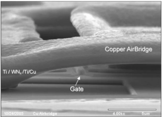
Fig. 2. SEM micrograph of the GaAs PHEMT with Cu airbridge using Ti/WNx/Ti/Cu multilayer system.
the Cu airbridges by PECVD to avoid the copper oxidation. The scanning electron microscopy (SEM) micrograph of the fabricated low-noise PHEMT with Cu airbridges is shown in Fig. 2.
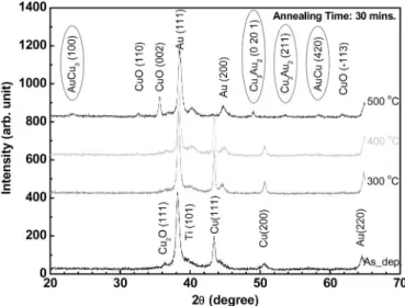
III. THERMALSTABILITY OF THEDIFFUSIONBARRIER Auger electron spectroscopy (AES) was used to analyze the depth profiles of the Ti/WNx/Ti/Cu multilayer system. The AES results for the Ti/WNx/Ti/Cu multilayer system before and after thermal annealing are shown in Fig. 3. It indicates that there is no interatomic diffusion between Cu and Au after an-nealing at 400◦C for 30 min. When the annealing temperature was increased to 500◦C, Cu and Au started to diffuse through the diffusion barrier layer. Fig. 4 shows the X-ray diffraction (XRD) patterns of the Ti/WNx/Ti diffusion barrier between Au and Cu layers before and after annealing. As can be seen, the Ti/WNx/Ti multilayer system was very stable after annealing at 300◦C and 400 ◦C and showed no interdiffusion between Cu and Au after the annealing. It proves that the Ti/WNx/Ti diffusion barrier was very effective in preventing Cu from dif-fusing into the Au layer even up to 400◦C annealing. However, additional peaks identified as Cu3Au2 and Cu–Au in Fig. 4
were observed after annealing at 500 ◦C. The Au was from the underlying Au-based contact metals, i.e., AuGeNiAu ohmic and Ti/Pt/Au gate. This was consistent with the AES depth profile analysis shown in Fig. 3(c), indicating the interdiffusion of Au and Cu across the Ti/WNx/Ti had occurred at 500◦C. The diffusion of the Au was from both ohmic and Schottky contacts (i.e., AuGeNiAu ohmic and Ti/Pt/Au gate metals). The top layers of the ohmic and gate metals are all Au metal. The transverse electromagnetic (TEM) cross section micrographs of the Ti/WNx/Ti diffusion barrier structure before and after 400◦C annealing are shown in Fig. 5(a) and (b), respectively. In Fig. 5(b), the interface of the WNxlayer was very sharp and no reaction between Ti, Au, Cu, and WNxlayers was observed. The TEM results are consistent with the above AES and XRD results. It shows that the Ti/WNx/Ti multilayer system is a very effective diffusion barrier structure between Cu and Au and is stable up to 400◦C annealing for 30 min.
Fig. 3. AES depth profiles of the Ti/WNx/Ti/Cu multilayer system (a) as
deposited, (b) after 400◦C annealing for 30 min, and (c) after 500◦C annealing for 30 min.
IV. ELECTRICALCHARACTERISTICS OF THE Cu-METALLIZEDAIRBRIDGEPHEMTS
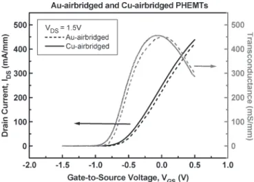
Electrical characteristics of both Cu- and Au-airbridged low-noise PHEMTs were measured and compared to evaluate the device performances after Cu metallization process. In the Fig. 6, the dc characteristics of the Cu-airbridged PHEMTs using Ti/WNx/Ti multilayer showed saturation drain–current (IDS) of 250 mA/mm when biased at VDS= 1.5 V. In order
to compare the dc characteristics of the Cu- and Au-airbridged PHEMTs, transconductance (gm) versus gate bias voltage
Fig. 4. XRD patterns of the Ti/WNx/Ti/Cu multilayer system after annealing
at different temperatures for 30 min.
Fig. 5. TEM cross section of Ti/WNx/Ti/Cu multilayer system (a) as
de-posited and (b) after 400◦C annealing for 30 min.
(VGS) curves of these two devices are shown in Fig. 7. The
maximum gmof the Cu-airbridged PHEMT with Ti/WNx/Ti diffusion barrier was 476 mS/mm. The gm, IDS, and pinchoff
voltage (Vp) of the Au- and Cu-airbridged PHEMTs were sim-ilar due to the Schottky contacts were with the same structure that was Ti/Pt/Au on AlGaAs.
There were two structures of thin-metal stacks, Ti/WNx/Ti and WNx (without Ti layer), for Cu-airbridged process that were studied to improve the performance and the uniformity
1756 IEEE TRANSACTIONS ON ELECTRON DEVICES, VOL. 53, NO. 8, AUGUST 2006
Fig. 6. Current–voltage curves of the low-noise Cu-airbridged PHEMTs with Ti/WNx/Ti/Cu as the thin-metal system.
Fig. 7. Transconductance (gm) versus gate bias voltage (VGS) of the
(a) Au-airbridged PHEMTs and the (b) Cu-airbridged PHEMTs with Ti/WNx/Ti multilayer.
of the Cu-airbridged PHEMTs. Histograms of the transconduc-tance (gm) and the pinchoff voltage (Vp) of the devices are shown in Figs. 8 and 9, respectively. Two half wafers from the same full 3-in wafer were processed, one half with the Ti adhesion layer and the other half without the Ti adhesion layer. The statistical data were collected from these two half wafers using semiautomatic probe system (SUSS PA200, KarlSuss) and wafer map software. A single die was probed from every 30-devices unit regularly arrayed on the wafer. More than 60 samples were measured across each half 3-in wafer. In Fig. 8, the average transconductance of the Cu-airbridged PHEMTs with Ti/WNx/Ti adhesion layer was 416 mS/mm, which was higher than that of the devices without Ti layer. The standard deviation of gm of the Cu-airbridged PHEMTs with Ti ad-hesion layer was 33 mS/mm, which was much smaller than that of the PHEMT without adhesion layer. The distribution of the pinchoff voltages for the Cu-airbridges and Au-airbridged PHEMTs are shown in Fig. 9. The pinchoff voltage of the Cu-airbridged devices with adhesion layer was distributed around
Vg =−0.7 to −0.8 V, and the standard deviation of the devices
Fig. 8. Histograms of the transconductance (gm) of the Cu-airbridged
PHEMTs with and without adhesion layer.
Fig. 9. Histograms of the pinchoff voltage (Vp) of the Cu-airbridged
PHEMTs with and without adhesion layer.
was 0.14 V, which was smaller than that without adhesion layer (0.22 V). According to the results of Figs. 8 and 9, higher yield and better uniformity of the Cu-airbridged PHEMTs was achieved by adding the Ti adhesion layers to the Au/WNx and WNx/Cu interfaces. The overall yield for the half piece with Ti adhesion layer was 86.5%, and the half piece without Ti adhesion layer was 67.7%. The Ti layer can improve the interfacial adhesion and avoid the metal peeling after thermal treatment.
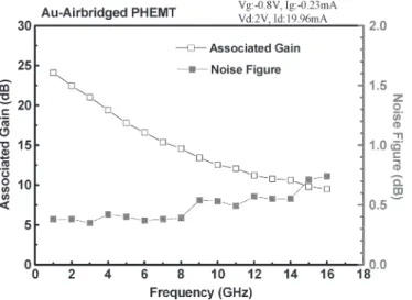
The noise figure and gain performances of the Au-airbridged low-noise PHEMTs are shown in Fig. 10. The noise figure is 0.74 dB and the associated gain is 9.2 dB at 16 GHz. Fig. 11 also shows the noise and gain performances of the Cu-metallized PHEMTs fabricated with and without the Ti adhesion layer. The noise figure of the device without Ti adhesion layer is 1.4 dB and the associated gain is 7.0 dB measured at 16 GHz. After adding Ti adhesion layers in the thin-metal structure, the noise figure and associated gain were improved by 0.76 and 8.8 dB, respectively. The performance of the Cu-metallized PHEMTs is improved by adding Ti adhesion layers. From the above results, the noise figure and the gain
Fig. 10. Noise figure and gain performances of the Au-metallized low-noise PHEMT.
Fig. 11. Noise figure and gain performances of the Cu-metallized low-noise PHEMT with and without Ti adhesion layer.
performances of the Cu-airbridged PHEMTs are comparable to those of the Au-airbridged PHEMTs after the insertion of the Ti adhesion layers in the Cu airbridge fabrication.
The current gain curves of the low-noise Au-airbridged and Cu-airbridged PHEMTs with and without the Ti adhesion layers are shown in Fig. 12. The three kinds of devices show similar performances. The cutoff frequency (fT) of the de-vices is all about 70 GHz. These results show that the Cu-airbridged PHEMTs with Ti adhesion layers in the thin-metal structure have comparable RF performance to conventional Au-airbridged PHEMTs.
V. CONCLUSION
The Cu airbridge interconnect process has been successfully applied to the fabrication of GaAs low-noise PHEMTs. WNx was used as the diffusion barrier and Ti was used as the adhesion layer to improve the adhesion between WNx/Cu interfaces in the thin-metal structure. From the results of AES depth profiles, TEM analysis, and XRD patterns, Ti/WNx/Ti multilayer system can sustain even after thermal annealing at 400 ◦C for 30 min. The GaAs PHEMTs fabricated with
Fig. 12. Cutoff frequency of the GaAs low-noise PHEMTs with Au and Cu airbridges.
Ti/WNx/Ti multilayer have higher gmand Vpuniformity than those of the GaAs PHEMTs with only WNxlayer. This is due to the improved adhesion of WNx diffusion barrier layer by the insertion of the Ti layers. The noise figure and the associ-ated gain of Cu-metallized PHEMTs were improved by 0.76 and 8.8 dB at 16 GHz, respectively, after using Ti/WNx/Ti multilayer system. The fT of the Cu- and Au-airbridged low-noise PHEMTs are about 70 GHz. The Cu-metallized low-low-noise GaAs PHEMTs have comparable electrical performances to those of the conventional Au-metallized devices. As a result, the Ti/WNx/Ti multilayer can serve as a good diffusion barrier for Cu metallization process for airbridge interconnects on the low-noise GaAs PHEMTs.
REFERENCES
[1] K. Holloway and P. M. Fryer, “Tantalum as a diffusion barrier between copper and silicon,” Appl. Phys. Lett., vol. 57, no. 17, pp. 1736–1738, Oct. 22, 1990.
[2] K. Holloway, P. M. Fryer, C. Cabral, Jr., J. M. E. Harper, P. J. Bailey, and K. H. Kelleher, “Tantalum as a diffusion barrier between copper and silicon: Failure mechanism and effect of nitrogen additions,” J. Appl. Phys., vol. 71, no. 11, pp. 5433–5444, Jun. 1992.
[3] C. Y. Chen, L. Chang, E. Y. Chang, S. H. Chen, and D. F. Chang, “Thermal stability of Cu/Ta/GaAs multilayers,” Appl. Phys. Lett., vol. 77, no. 21, pp. 3367–3369, Nov. 2000.
[4] D. S. Yoon, H. K. Baik, and S. M. Lee, “Effect on thermal stability of a Cu/Ta/Si heterostructure of the incorporation of cerium oxide into the Ta barrier,” J. Appl. Phys., vol. 83, no. 12, pp. 8074–8076, Jun. 1998. [5] E. R. Weber, “Transition metals in silicon,” Appl. Phys. A, Solids Surf.,
vol. 30, no. 1, pp. 1–22, Jan. 1983.
[6] A. Cros, M. O. Aboelfofotoh, and K. N. Tu, “Formation, oxidation, elec-tronic, and electrical properties of copper silicides,” J. Appl. Phys., vol. 67, no. 7, pp. 3328–3336, Apr. 1, 1990.
[7] C. Y. Chen, E. Y. Chang, L. Chang, and S. H. Chen, “Backside Cu metallization of GaAs MESFETs using TaN as the diffusion barrier,” IEEE Trans. Electron Devices, vol. 48, no. 6, pp. 1033–1036, Jun. 2001. [8] H. C. Chang, E. Y. Chang, Y. C. Lien, L. H. Chu, S. W. Chang, R. C.
Huang, and H. M. Lee, “Use of WNxas diffusion barrier for Cu airbridged
low noise GaAs PHEMT,” Electron. Lett., vol. 39, no. 24, pp. 1763–1765, Nov. 2003.
[9] P. H. Wohlbier, “Diffusion and defect data,” Trans. Tech., vol. 10, no. 1–4, pp. 89–91, 1975.
[10] P. Madakson and J. C. Liu, “Interdiffusion and resistivity of Cu/Au, Cu/Co, Co/Au and Cu/Co/Au thin films at 25–550◦C,” J. Appl. Phys., vol. 68, no. 5, pp. 2121–2126, Sep. 1990.
1758 IEEE TRANSACTIONS ON ELECTRON DEVICES, VOL. 53, NO. 8, AUGUST 2006
Cheng-Shih Lee was born in Taiwan, R.O.C. He
received the Ph.D. degree in materials science and engineering from the National Sun Yat-Sen Univer-sity, Kaohsiung, Taiwan, in 1999.
He is currently a Research Associate in the De-partment of Materials Science and Engineering at National Chiao-Tung University, Hsinchu, Taiwan, R.O.C. His research interests are millimeter-wave package, and fabrication and characterization of compound semiconductor devices.
Yi-Chung Lien received the B.S. and M.S.
de-grees from Da-Yeh University, Chang-Hua, Taiwan, R.O.C., in 1999 and 2001, respectively, all in electri-cal engineering. He is currently working toward the Ph.D. degree in the Department of Materials Science and Engineering at National Chiao-Tung University, Hsinchu, Taiwan.
His research interests are fabrication and charac-terization of HEMT for high-frequency applications.
Edward Yi Chang (S’85–M’85–SM’04) received
the B.S. degree from National Tsing-Hua University, Hsinchu, Taiwan, R.O.C., in 1977, and the Ph.D. de-gree from the University of Minnesota, Minneapolis, in 1985, all in materials science and engineering.
From 1985 to 1988, he was with Unisys Cor-poration GaAs Compound Semiconductor Group, Eagan, MN, and from 1988 to 1992, he was with Comsat Labs Microelectronic Group. He worked on the GaAs monolithic microwave integrated circuit (MMIC) programs in both groups. In 1992, he joined National Chiao-Tung University, Hsinchu. In 1994, he helped set up the first GaAs MMIC production line in Taiwan, and became President of Hexawave Inc., Hsinchu, in 1995. He returned to the teaching position in National Chiao-Tung University in 1999 and is currently Professor and Department Head of the Department of Materials Science and Engineering. His research interests include new devices, process, and packaging technologies for III–V-based radio frequency integrated circuits (RFICs) for wireless communication.
Dr. Chang is a senior member of the IEEE Electron Devices Society.
Huang-Choung Chang was born in Taiwan, R.O.C.
He received the Ph.D. degree in materials science and engineering from the National Chiao-Tung Uni-versity, Hsinchu, Taiwan, in 2004.
His research interests are fabrication and charac-terization of compound semiconductor devices and copper metallization of GaAs devices.
Szu-Houng Chen was born in Taiwan, R.O.C.
He received the B.S. degree from National Tsing-Hua University, Hsinchu, Taiwan, in 1977, and the Ph.D. degree from National Chiao-Tung University (NCTU), Hsinchu, in 2002, all in materials science and engineering.
Since 2003, he has been with the Compound Semi-conductor Device Laboratory (CSDLAB), NCTU as a Postdoctoral Researcher. His research interests are in the area of new materials and process tech-nologies for compound semiconductor devices and high-speed device technologies.
Ching-Ting Lee (M’89–SM’97) was born in
Taoyuan, Taiwan, R.O.C., on November 1, 1949. He received the B.S. and M.S. degrees from the De-partment of Electrical Engineering, National Cheng-Kung University, Tainan, Taiwan, in 1972 and 1974, respectively, and the Ph.D. degree from the Depart-ment of Electrical Engineering, Carnegie–Mellon University, Pittsburgh, PA, in 1982, all in electrical engineering.
In 1990, he was with the Chung Shan Institute of Science and Technology, before he joined the Insti-tute of Optical Sciences, National Central University, Chung-Li, Taiwan, as a Professor. In 2003, he was with National Cheng-Kung University as the Dean of Electrical Engineering and Computer Science and a Professor with the Institute of Microelectronics, Department of Electrical Engineering. His current research interests include theory, design, and application of guided-wave structures and devices for integrated optics and waveguide lasers. His research activities involve research concerning semiconductor lasers, photodetectors, and high-speed electronic devices, and their associated integration for electrooptical integrated circuits.
Dr. Lee received the Outstanding Research Professor Fellowship from the National Science Council (NSC), Taiwan, in 2000 and 2002. He also received the Optical Engineering Medal from the Optical Engineering Society and the Distinguish Electrical Engineering Professor Award from the Chinese Institute of Electrical Engineering Society in 2003.
Li-Hsin Chu was born in Taiwan, R.O.C. He
re-ceived the B.S. degree from the National Chiao-Tung University (NCTU), Hsinchu, Taiwan, in 2000. He is currently working toward the Ph.D. degree in materials science and engineering at NCTU.
His research interests are fabrication and charac-terization of enhancement-mode power HEMT.
Shang-Wen Chang was born in Taiwan, R.O.C.
He received the M.S. degree in physics from the National Taiwan University, Taipei, Taiwan, in 2000. He received the Ph.D. degree in materials science and engineering at National Chiao-Tung University, Hsinchu, Taiwan, in 2005.
His research interests are fabrication and charac-terization of compound semiconductor devices and copper metallization of GaAs devices.
Yen Chang Hsieh was born in Taiwan, R.O.C. He
re-ceived the M.S. degree in physics from the National Chung Hsing University, Taichung, Taiwan, in 2001. He is currently working toward the Ph.D. degree in materials science and engineering at National Chiao-Tung University, Hsinchu, Taiwan.
His research interests are growth of III–V epitaxial material on Si substrates for high-speed electronic applications.