AI203 Films Formed by Anodic Oxidation of
AI-1 Weight Percent Si-0.5 Weight Percent Cu Films
Re-Long Chiu and Peng-Heng Chang
Institute of Materials Science and Engineering, National Chiao Tung University, Hsinchu, Taiwan 30049
Chih-Hang Tung
Electronics Research and Service Organization, Industrial Technology Research Institute, Chu-Tung, Taiwan 31015
ABSTRACT
The structure of the barrier-type anodic oxide formed on preannealed Al-1 weight percent (w/o) Si-0.5 w/o Cu t h i n film in a tartaric acid electrolyte was investigated. The oxide film is basically an amorphous layer with a thin dispersed ~'-A1203 crystalline layer interposed in the center. Pores are observed to be associated with the -y'-A1203 layer. Silicon nodu]es and A12Cu particles originally present in the AI-1 w/o Si-0.5 w/o Cu film behave differently during anodization. Silicon nodules are oxidized to various degree during anodizing. The silica formed in the Si nodules is amorphous a n d somewhat porous possibly due to oxygen evolution associated with the Si anodization. A dark rim was found to surround each nodule in the anodic oxide film. This rim is shown to be thicker amorphous A120~ material, and its origin is a t t r i b u t e d to the faster oxidation rate in the vicinity of Si nodules. A12Cu precipitates are oxidized to form A1203 at about the same rate as the s u r r o u n d i n g A1 matrix. Copper is rejected by A1203 a n d accumulates at the A12OJA1 interface.
Introduction
To m a k e large size panels a n d high resolution thin-film transistors (TFT) for liquid crystal display (LCD), w e m u s t choose a metal with l o w resistivity for the reduction of gate pulse delay a n d of w a v e f o r m distortion. I'2 T h e resistivity of the gate bus-line metal used in traditional panel displays, such as Cr or Ta, is too high to m e e t the requirement. 3 T h e l o w resistivity a n d the well-established process technology of Al m a k e s it an attractive choice for this application. H o w e v e r , the propensity of hillocks formation in thin-film A1 metal on Si substrate during heat processing, until re- cently, has prevented their applications in T F T / L C D . Hillocks generally f o r m on Al films to relieve planar c o m - pressive stresses introduced either during deposition or subsequently b y substrate-induced differential thermal e x p a n s i o n strains. 4 Recently, it w a s reported I that AI an- odic oxide film can w o r k as a protective layer against hillock formation. Thin-film transistors with A1 gate a n d an anodic A1203 + S i N double-layer gate insulator h a v e b e e n applied successfully to the 10.4 in. diagonal multi- color L C D display panel. I
T h e anodic oxidation of Al a n d its alloys has b e e n studied extensively for applications requiring corrosion resistance, abrasive resistance, electrical insulation, a n d decorative coloring, etc. Literature is readily available w h i c h provides recipes for p r o d u c i n g various kinds of anodic a l u m i n u m
oxide coatings. 5'~ Basically, t w o types of anodic oxide film can be f o r m e d o n Al d e p e n d i n g o n electrolytes used. 5 For solvent electrolytes, such as sulfuric acid, oxalic acid, c h r o m i c acid, phosphoric acid, etc., the acid solutions h a v e a solvent effect on the oxide film a n d thus thick porous oxide films are produced. F o r nonsolvent electrolytes, e.g., boric acid a n d tartaric acid, thin impervious oxide films are f o r m e d (typically referred to as barrier films~). T h e barrier
120 t
I 0"04
,
-
-
.
1
0
0
~
I0"03
0.02
0
500
1000
1500
2000
Time (sec)
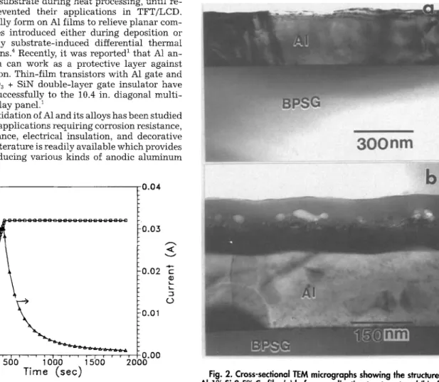
Fig. 1. Variation of potential and current with time during anodizing.
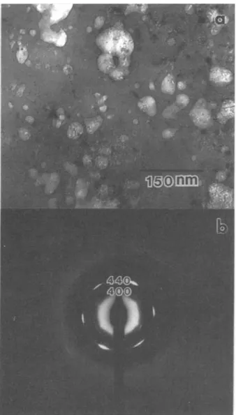
Fig. 2. Cross-sectional TEM micrographs showing the structure of A1-1% Si-0.5% Cu film (a) before anodization treatment and (b) after anodization treatment.
J. Electrochem. Soc.,
Vol. 142, No. 2, February 1995 9 The Electrochemical Society, Inc
525
) unless CC License in place (see abstract). ecsdl.org/site/terms_use
address. Redistribution subject to ECS terms of use (see 140.113.38.11
density a n d increasing voltage. 9'~~ Crystalline film has a higher capacitance because of larger dielectric constant, ~~ but it exhibits an electrical instability ~ w h i c h are related to the presence of voids ~2 and/or to the trapped oxygen. 13 This instability, however, can be r e m o v e d b y a relaxation a n d reanodization treatment. ~ T h e crystalline oxide for- m a t i o n is retarded b y the anion incorporation f r o m elec- trolytes. ~4 T h e effect of alloying elements o n crystalline ox- ide formation varies, for example, M g promotes, but Si a n d C u h a m p e r s , the ~/'-AI2Q formation. ~5 L e a c h a n d P e a r s o n ~6 h a v e correlated the crystallization of various anodic metal oxide to the presence of compressive stress in the film. F o r anodic a l u m i n u m oxide, it is generally agreed that the stress in the film is compressive during anodizing d u e to electrostrietion, but it rapidly changes to tensile in the
150 100- ~ 0 - 0 c AJ d i I i J C u
A
L
4 8 4 8 0 4 8~ ( ~ )
~ ( ~ )
E ~ ( ~ )
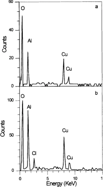
Fig. 4. XTEM micrograph showing (a) AI2Cu precipitate and (b) Si
nodules in aluminum films before anodizing. (c}, (d), and (e} are EDX
spectra obtained from the AI film matrix, the particle shown in (a),
and the particle shown in (b), respectively.
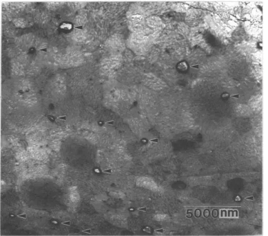
Fig. 3. (a) Planar TEM micrograph showing the structure of the
AI~O3 film where voids and particles are present. (b) Electron diffrac-
tion pattern obtained from the region shown in (a). The ring pattern
shows that the particles are "y'-AI203.
open-circuit condition. 17-~9 Nelson and Oriani 19 have pro- posed a model which relates the sign and the magnitude of the stress to the Pilling-Bedworth ratio (the ratio of the volume of the oxide formed to the volume of the metal oxidized) of the metal and the transport n u m b e r of the anion in the oxide. They also showed t h a t the open-circuit stress of anodic aluminum oxide film changes from tensile to compressive when the anodizing current density is < - 0 . 5 m A c m -2.
For integrated circuit applications, aluminum metalliza- tion is often doped with small amounts of Si and/or Cu to control aluminum spiking 2~ and electromigration. 21 Cop- per-doped A1 film has an added advantage of improved resistance to hillock formation. 22 Therefore, it is of great interest to investigate the anodic oxide formed in A1 thin films doped with Si and Cu. In this paper, we undertake to study A1203 layers formed by anodic oxidation of A1-1% Si-0.5% Cu films. Special emphasis is given to the effect of Si and Cu doping on the oxidation behavior.
Experimental
The substrates for this study are 100 m m diam, p-type, <100>, Si wafers. To simulate a typical glass substrate used for LCD display, the Si substrates were first thermally oxi- dized to form a 550 nm thermal oxide followed by chemical v a p o r deposition (CVD) of a 600 nm thick borophosphosili- care glass (BPSG) at 720~ A 300 nm thick AI-Si-Cu film was subsequently deposited in a dc magnetron sputtering deposition machine from an AI-1 w/o St-0.5 w/o Cu target on top of the B P S G layer. The samples were then annealed in nitrogen for 30 min at 410~ A1203 insulating layer was grown by anodizing the A1-Si-Cu layer sputtered on B P S G / SiO2/Si substrates. Anodization was conducted in AG'vV electrolyte ~3 which is a mixture of 3% aqueous solution of tartaric acid and propylene glycol at a volume ratio of 2 to 8. Constant current mode (current density = 0.4 mA cm -2) was employed initially until the potential reached 100 V, then the experiment was changed to constant voltage mode. The total time of anodization was 30 rain and the current density eventually was decreased to 0.015 m A c m ~.
) unless CC License in place (see abstract). ecsdl.org/site/terms_use
address. Redistribution subject to ECS terms of use (see 140.113.38.11
J. Electrochem. Soc.,
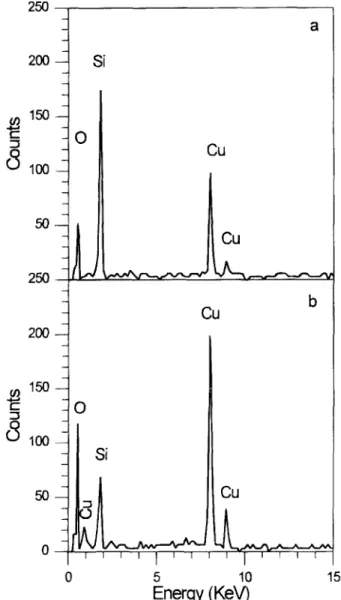
Vol. 142, No. 2, February 1995 9 The Electrochemical Society, Inc. 527Fig. 5. Planar TEM micragraph
of the Ai203 layer near its top sur-
face. Larger rimmed nodules (ar-
rowed) are visible.
Figure 1 shows the variation of voltage a n d current as a function time from a typical anodizing run.
The structure of the films before a n d after anodization subsequently was studied by transmission electron mi- croscopy (TEM). Both cross-sectional a n d p l a n a r TEM samples were prepared by ion milling in the usual fashion 2~ a n d examined with a Philips CM20 microscope operating at 160 kV. Energy dispersive x-ray (EDX) analysis was per- formed using EDAX 9800 with a windowless detector at- tached to the Philips CM20 microscope. The chemical com- positions of the films before a n d after anodization were profiled by secondary ion mass spectrometry (SIMS) with a VG SIMSLAB 3B using O~ probe at 8 keV, 600 nA.
Results and Discussion
Figure 2a shows a cross-sectional TEM (XTEM) mi- crograph of the as-deposited A1-Si-Cu film after a n n e a l i n g at 410~ for 30 rain a n d subsequently furnace cooled. Fig- ure 2b shows the oxide layer formed after the 30 m i n anodic oxidation treatment. The thickness of the as-deposited Al- Si-Cu film is - 3 0 0 n m as measured from Fig. 2a. After the anodic oxidation, the thickness of the remaining Al film is - 2 1 0 n m while the anodic oxide layer is - 1 3 0 nm. Assum- ing the i n i t i a l A1 thickness is constant across the samples, this means that 90 n m thick A1 has been converted to form 130 n m of A1203, indicating a Pilling-Bedworth ratio of 1.44 which is close to the value reported of crystalline anodic A1203.18 Pringle25 has suggested the use of "nm/V" value (the ratio between the oxide thickness in nanometers a n d the potential drop across the oxide in volts) as a measure of the resistivity of the oxide. The nm/V value for our anodic oxide is 1.3 which is in excellent agreement with the value of 1.29 reported for a typical anodic a l u m i n u m oxide. 2~ The anodic oxide film is mostly amorphous b u t crystalline par- ticles a n d voids are readily visible near the middle of the amorphous film as clearly revealed in the XTEM mi- crograph of Fig. 2b. Figure 3a shows a p l a n a r view of the anodic oxide film n e a r its center where voids a n d crys- talline particles are present. The white blobs i n Fig. 3a cor- respond to the voids in the .middle of the oxide layer shown in Fig. 2b. The voids are typically associated with small
dark particles. Selective area diffraction p a t t e r n obtained from this region (Fig. 3b) reveals that these particles are '-A1203. From Fig. 3a, the size of the ~]'-A1203 particles is estimated to be less t h a n 30 nm. Voids associated with crys- talline A120~ in the middle of the amorphous A1203 layer have been observed by m a n y investigators 8'9'26 in anodically formed A1203 films. The origin of the voids is not clear yet, b u t two models have been suggested in the literature: (i) voids are due to the volume contraction caused by the amorphous to crystalline transformation, 8 or
(ii)
oxygen generated during anodization process tends to be trapped near the crystalline A1203 particles a n d eventually results in the formation of voids a r o u n d t h e m ? It has been shown convincingly that the location of the crystalline A1203 par- ticles corresponds to the original top surface of the A1 layer where crystalline nuclei are formed during thermal oxida- t i o n ? '14'28 Subsequent anodization proceeds in a typical ionic transport mechanism 14'~5 in which amorphous oxide grows at the oxide/electrolyte a n d metal/oxide interfaces by the outward migration of metal a n d i n w a r d migration of oxygen, respectively. At appropriate anodizing voltage (which varies with electrolyte), ~ ' - A l 2 Q grows on the exist- ing ~-A1203 nuclei a n d thus a final amorphous/crystalline/ amorphous sandwich structure of A1~O3 is developed.A l u m i n u m films doped with Si and Cu in excess of their solubility limits generally contain precipitates in the form of Si nodules 27 a n d Al2Cu particles. 2~ These two types of precipitates were observed in the as-deposited AI-Si-Cu films, as shown in Fig. 4. The identification of different phases in a TEM sample is accomplished most easily by EDX, a n d Fig. 4c-e are EDX spectra obtained from the Al film m a t r i x shown in Fig. 4a, the particle shown in Fig. 4a, a n d the particle shown in Fig. 4b, respectively. Since the doping level of Si a n d of Cu is below the detection limit of EDX in our specimens, the weak Cu peak at 8.04 keV in Fig. 4c is due not to the Cu doping in the film b u t to the sporadic scattering from the Cu supporting ring on which the t h i n TEM sample is mounted. The coexistence of the strong Al a n d Cu peaks i n Fig. 4d is an indication that the particle shown i n Fig. 4a is Al2Cu. The d o m i n a n t Si peak in Fig. 4e proves that the particle in Fig. 4b is a n Si nodule. It
) unless CC License in place (see abstract). ecsdl.org/site/terms_use
address. Redistribution subject to ECS terms of use (see 140.113.38.11
unambiguously to the [111] zone axis of Si while the faint ring p a t t e r n is due to the underlying unreacted A1 sub- strate. This proves that the dark region is crystalline Si. The lighter regions which do not show a n y diffraction con-
50
2 5 0 - -
2 0 0 - -.~ 150--
8 loo
50
0b
Cu
O
Si
=~
Cu
0
5
10
15
Energy
(KeV)
Fig. 7. EDX spectra from (a) the dark region inside the rimmed nodule of Fig. 6a, and (b) the lighter region inside the rimmed nodule of Fig. 6c.
Fig. 6. (a) Blowup view of the rimmed nodules shown in Fig. 5. (b) Electron diffraction pattern obtai_ned from the dark inner region of (a), the spot pattern is due to Si [111] zone and the faint ring pattern is due to the underlying unreacted AI layer. (c) Another rimmed nodule with most of its Si content oxidized.
trast are m o s t likely a m o r p h o u s in nature. T h e relative a m o u n t of the dark a n d lighter regions in the r i m m e d n o d u - lar precipitates varies significantly. Figure 6c s h o w s a sim- ilar precipitate in w h i c h the inner region is c o m p o s e d mostly of a light a m o r p h o u s phase, but a small d a r k patch of material ( m a r k e d b y arrow) can be observed at the u p p e r right. This d a r k patch is identified as Si b y electron diffrac- tion. To identify the lighter a m o r p h o u s p h a s e w e resorted to the E D X technique. Figures 7a a n d b are the E D X spec- tra obtained f r o m the dark region in Fig. 6a a n d the lighter region in Fig. 6c, respectively. T h e C u peaks w h i c h are present in all the E D X spectra here are mostly artifacts f r o m the T E M s a m p l e holder. N o Al signal is detected in these regions. Consistent with the electron diffraction re- sult s h o w n in Fig. 6b, the m a j o r strong p e a k in Fig. 7a is d u e to Si, indicating the dark area is primarily St. T h e small o x y g e n p e a k in Fig. 7a is indicative of the presence of a small a m o u n t of silicon oxide. T h e s p e c t r u m in Fig. 7b also consists of Si a n d o x y g e n peaks, but the o x y g e n p e a k inten- sity is m u c h higher than that of the Si peak. This implies that the region is m a d e mostly of silicon oxide. B a s e d on the electron diffraction a n d E D X results w e conclude that the r i m m e d nodular precipitates in the anodie oxide film are Si nodules oxidized to various degrees. T h e standard free- energy of formation is higher for SiO2 than for A1203, 29 so A1 matrix is oxidized prior to Si nodules during anodiza- tion. B u t the indiffusing o x y g e n eventually oxidizes the Si nodules at different depths to various degrees, thus f o r m i n g nodules consisting of mixtures of crystalline Si a n d silicon
) unless CC License in place (see abstract). ecsdl.org/site/terms_use
address. Redistribution subject to ECS terms of use (see 140.113.38.11
J. Electrochem. Soc., Vol. 142, No. 2, February 1995 9 The Electrochemical Society, Inc. 529
8
0 --
40
8
"
2 0 - -
_
1 0 0 -
50
O
a
AJ
p,,. mO
C ub
AI
CA
Cu
C U 0 0 5 10 15Energy (KeV)
Fig. 8. EDX spectra from (a) the dark rim of the rimmed nodule and
(b) the neighboring AI203 matrix.
oxide of various proportions such as those observed in Fig. 6a a n d c.
T h e nature of the d a r k rims surrounding the St/silica nodules is m o r e difficult to analyze. Despite n u m e r o u s at- tempts, n o electron diffraction pattern could be obtained f r o m the d a r k r i m region, indicating that it is p r o b a b l y a m o r p h o u s . (To substantiate this conjecture w e point out that n o diffraction contrast w a s ever observed in the d a r k r i m region either.) E D X analysis w a s c o n d u c t e d on the r i m region in the h o p e of getting s o m e ideas about its chemistry, a n d a typical s p e c t r u m is s h o w n in Fig. 8a. W e see f r o m the s p e c t r u m that the m a j o r constituents of the r i m region are
Fig. 9. XTEM micrograph showing a rimmed nodule in the AI2Os film.
1 5 0 ..
Cu
b
1 0 0 -8
5 0 -o
~
I ] t ] l I I 0 5 10Energy
(Kev)
Fig. 10. (a) XTEM micrograph showing AI203 film cutting through
an AI2Cu precipitate originally present in the aluminum film. (b) The
EDX spectrum obtained from the AI2Cu precipitate shown in (a).
A] a n d oxygen. F o r comparison, a n E D X s p e c t r u m f r o m the neighboring A1203 matrix is s h o w n in Fig. 8b. T h e t w o spec- tra are simi]ar except that the o x y g e n content s e e m s to be higher in the r i m region than in the matrix (the extra C1 p e a k at 2.62 k e V in Fig. 8b probab]y is d u e to c o n t a m i n a - tion of the T E M s a m p l e during handing). T h e s e results strongly suggest that the dark r i m is also a l u m i n u m oxide. Figure 9 s h o w s an XTEIVi m i c r o g r a p h of a r i m m e d particle in the A1203 layer. This particle w a s originally an Si nodule -0.65 p.m in size w h i c h w a s located at the film surface initially. T h e top portion of the nodule apparently has b e e n
I
0 s
c '7 o L) 1 0 41 0 s
1
0 ~ 1011 0 ~
A,:,
Si
f
Si
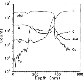
0 AIAI Cu 0 200 400 600Depth
(nm)
Fig. 11. SIMS profile of the sample bo~re anodizafion.
) unless CC License in place (see abstract). ecsdl.org/site/terms_use
address. Redistribution subject to ECS terms of use (see 140.113.38.11
101 10 ~ Cu Cu 2 0 0 4 0 0 6 0 0
Depth (nm)
Fig. 12. SIMS profile of the sample after anodizafion.
oxidized to a porous and amorphous silica structure while its b o t t o m remains crystalline St. The thickness of the A1203 layer at the vicinity of the particle is much l a r g e r t h a n regions a w a y from the particle, thus forming an A1203 spike a r o u n d the particle. On comparing the morphology of the
r i m m e d particle shown in Fig. 9 to the one shown in Fig. 6a, it is a p p a r e n t t h a t the rim is also A1203 a n d it a p p e a r s to be d a r k e r because of its larger thickness. Rimmed Si nodules oxidized to various degrees have been observed b y Shimizu
e t al. 3~ in b u l k b i n a r y A1-1.5% Si alloy anodized in 0.1M a m m o n i u m b o r a t e solution. Thicker A1303 film growth in regions surrounding the Si particle also was observed and was ascribed to the local current concentration effects (such as heating) at the Si particle during anodizing. 3~ The porous n a t u r e of the amorphous silica observed here likely is due to the oxygen evolution during the o x i d a t i o n of Si nodules, a phenomenon reported in the anodizing of Al al- loys containing 8.5 to 10% Si in a 5 w/o ammonium p e n t a b - orate solution. 31 Due to their cross-sectional TEM sample p r e p a r a t i o n technique (which is performed b y u l t r a m i c r o - tomed sectioning in contrast to ion milling used here), Shimizu et al. 3o were u n c e r t a i n about the n a t u r e of the d a r k rims and thought t h a t they m a y "merely reflect some arti- fact developed during sectioning." Since ion milling is much less prone to artifacts t h a n u l t r a m i c r o t o m e d section- ing, the present result in a w a y confirms unequivocally the presence of thicker oxide rims a r o u n d Si nodules.
A12Cu precipitates behaved in a t o t a l l y different w a y from t h a t of Si nodules during anodizing. Figure 10a shows an anodic oxide, - 1 4 0 nm thick, formed on top of the A1- Si-Cu layer. The EDX spectrum in Fig. 10b is obtained from the b l a c k particle in the A1 layer, and the strong Al and Cu peaks in this spectrum are a clear indication t h a t the p a r t i - cle is an A12Cu precipitate. This A12Cu particle is originally present in the A1-Si-Cu film p r i o r to anodization, b u t is cut through b y the advancing oxide film. F r o m the morphology of the A12Cu particle it is a p p a r e n t t h a t the top p o r t i o n of it has been oxidized. The TEM structure of the anodic oxide directly on top of the A12Cu particle is not different from the oxide m a t e r i a l which is directly on top of A1. Also, the A12OJA1 interface is smooth across the Al2Cu particle. These results seem to indicate t h a t the o x i d a t i o n rate is c o m p a r a b l e for the A l - l % Si-0.5% Cu m a t r i x and the A12Cu precipitates in our films. By EDX, we have checked the b u l k chemistry of the A1203 m a t e r i a l directly on top of the p r e c i p i t a t e and found no significant difference from regions directly on top of the A1. The oxide film directly on top of the A12Cu particle is not enriched in Cu. F u r t h e r insight of the change in film chemistry due to anodization can be obtained from SIMS analysis. Figures 11 and 12
profiling. The Cu signal in the anodic oxide layer is a p p a r - ently one to two orders of m a g n i t u d e lower t h a n the Cu signal in the remaining unreacted A1 layer as shown in Fig. 12. A notable Cu p e a k is observed also at the A12OJA1 interface. These results strongly suggest t h a t the solubility of Cu in A1203 is lower t h a n in A1. Copper is rejected b y A1203 and b u i l d s up at the interface during anodization. It is likely t h a t when the advancing A12OJA1 interface en- counters an A12Cu p r e c i p i t a t e during anodization, dissoci- ation of A12Cu to Al and Cu occurs first; and A1 subse- quently is converted to A1203 while Cu is rejected to the interface. The rejection of Cu b y the anodic aluminum ox- ide and the accumulation of Cu at the A120:JA1 interface have been observed previously by S t r e h b l o w et al. 32 in sputter deposited A1-Cu films using Rutherford b a c k s c a t - tering spectrometry (RBS). These authors have speculated t h a t the f o r m a t i o n of copper-enriched metal intrudes into
the oxide p h a s e leading to the b r e a k d o w n of the anodic film, b u t this hypothesis is not supported by our TEM ob- servation which shows a flat interface even at the vicinity of an A12Cu precipitate. Although there is Cu accumulation at the o x i d e / m e t a l interface, the cross-sectional TEM re- sults clearly rule out the existence of any identifiable phase due to the excess Cu concentration.
Conclusion
0
The anodic oxide formed on AI-1 Yo Si-0.5% Cu thin film is b a s i c a l l y an amorphous l a y e r with a thin ~'-A120~ crys- talline layer interposed in the center. Pores are observed to be associated w i t h the ~'-A1203 layer. The 410~ p r e a n - healed Al films contain precipitates of A12Cu particles and Si nodules. Silicon nodules are oxidized to various degrees during anodizing. The silica formed in the Si nodules is amorphous and a d a r k r i m surrounded each nodule. The d a r k rim is thicker amorphous A1203 material, and its origin is a t t r i b u t e d to the faster o x i d a t i o n r a t e in the vicin- ity of Si nodules. The faster o x i d a t i o n rate p r o b a b l y is due to the localized Joule heating caused by the local current concentration induced b y the presence of Si nodules. The silica structure is s o m e w h a t porous which can be e x p l a i n e d b y the oxygen evolution associated w i t h the anodization of St. A12Cu precipitates are oxidized to form A1203 at about the same rate as the surrounding A1 matrix. Copper oxide is n o t detected in the anodic A1203 films. The solubility of Cu in A120~ is lower t h a n t h a t in A1 so t h a t copper is re- jected b y Al2Q and accumulates at the A1203/A1 interface.
Acknowledgment
This w o r k was s u p p o r t e d in p a r t b y the N a t i o n a l Science Council, Taiwan, Republic of China, through G r a n t No. NSC 83-0404-E-009-098. We express our a p p r e c i a t i o n to one of the reviewers who directed our attention to the w o r k of S t r e h b l o w et al. on A1-Cu films.
Manuscript s u b m i t t e d Jan. 28, 1994; revised m a n u s c r i p t received Sept. 7, 1994.
N a t i o n a l Chiao T u n g U n i v e r s i t y a s s i s t e d i n m e e t i n g t h e p u b l i c a t i o n c o s t s o f t h i s article.
REFERENCES
1. H. Yamamoto, H. Matsumaru, K. Shirahashi, M. Nakatani, A. Sasano, N. Konishi, K. Tsutsui, and T. Tsukada, 1990 Int. E l e c t r o n D e v i c e Meet., Techn. D i - gest, 851 (1990).
) unless CC License in place (see abstract). ecsdl.org/site/terms_use
address. Redistribution subject to ECS terms of use (see 140.113.38.11
J. Electrochem. Soc., Vol. 142, No. 2, February 1995 9 The Electrochemical Society, Inc.
531
2. T. Sunata, T. Yukawa, K. Miyake, Y. Matsushita, Y.Murakami, Y. Ugai, J. Tamamura, and S. Aoki,
IEEE
Trans. Electron Devices,
ED-33, 1212 (1986). 3. W. J. Sah, J. L. Lin, and S. C. Lee,ibid.,
ED-38, 676(1991).
4. C. Y. Chang and R. W. Vook,
Thin Solid Films,
228, 205 (1993).5. V. F Henley,
Anodic Oxidation of Aluminum & Its Al-
loys,
Pergamon Press, Oxford (1982).6. S. Wernick, R. Pinner, and P. G. Sheasby,
The Surface
Treatment and Finishing of Aluminum and Its Al-
loys,
5th ed., Finishing Publ. Ltd., Teddington, Eng- l a n d (1987).7. S. Sato, H. Ichinose, and N. Masuko,
This Journal,
138, 3705 (1991).8. K. K o b a y a s h i a n d K. Shimizu, in
Aluminum Surface
Treatment Technology,
R. S. A l w i t t and G. E. T h o m p - son, Editors, PV 86-11, p. 380, The Electrochemical Society Proceedings Series, Pennington, NJ (1986). 9. C. Crevecoeurs and H. J. de Wit,This Journal,
134, 808(1987).
10. C. T. Chen a n d G. A. Hutchins,
ibid.,
132, 1567 (1985). 11. R. S. A l w i t t and C. K. Dyer,Electrochim. Acta,
23, 355(1978).
12. R. S. Alwitt, C. K. Dyer, and B. Noble,
This Journal,
129, 711 (1982).
13. W. J. B e r n a r d and R G. Russell,
ibid.,
127, 1256 (1980). 14. G. E. Thompson and G. C. Wood, inTreatise on Materi-
als Science and Technology,
Vol. 23, J. C. Scul]y, E d i - tor, p. 205, Academic Press, London (1983).15. M. J. Dignam,
This Journal,
109, 184 (1962).16. J. S. Leach and B. R. Pearson,
Corros. Sci.,
26, 43 (1988).17. R. S. Alwitt, J. Xu, and R. C. McClung,
This Journal,
140, 1241 (1993).
18. N. Wuthrich,
EIectrochim. Acta,
26, 1617 (1981). 19. J. C. Nelson and R. A. Oriani,Corros. Sci.,
34, 309(1993).
20. R H. Chang, R. Hawkins, T. D. Bonifield, and L. A. Melton,
AppI. Phys. Lett.,
52, 272 (1988).21. P. B. Ghate, in
Proceedings of the IEEE International
Reliability Physics Symposium,
p. 243 (1981). 22. S. Wolf and R. N. Tauber,Silicon Processing for the
VLSI Era,
Vol. 2, p. 271, Lattice Press, California (1990).23. H. Hasegawa and H. L. Hartnagel,
This Journal,
123, 713 (1976).24. R H. Chang, H. Y. Liu, J. A. Keenen, and J. M. Anthony,
J. Appl. Phys.,
62, 2485 (1987).25. J. R Pringle,
Electrochim. Acta,
25, 1423 (1980). 26. K. K o b a y a s h i and K. Shimizu,This Journal,
135, 908(1988).
27. C. H. Tung, C. T. Chang, H. C. Chang, S. Chiu, B. Kou, and L. S. Chang,
J. Appl. Phys.,
68, 1592 (1990). 28. D. R. Frear, J. E. Sanchez, A. D. Romig, Jr., and J. W.Morris, Jr.,
Met. Trans.,
A21, 2449 (1991).29. L. S. D a r k e n and R. W. Gurry,
Physical Chemistry of
Metals,
p. 349, M c G r a w - H i l l Book Co., New York (1953).30. K. Shimizu, G. E. Thompson, and G. C. Wood,
Elec-
trochim. Acta,
27, 245 (1982).31. H. S. Kim, G. E. Thompson, G. C. Wood, I. G. Wright, and R. E. Marringer,
Trans. Inst. Met. Finish.,
62, p a r t 2, 49 (1984).32. H.-H. Strehblow, C. M. Melliar-Smith, and W. M. Augustyniak,
This Journal,
125, 915 (1978).) unless CC License in place (see abstract). ecsdl.org/site/terms_use
address. Redistribution subject to ECS terms of use (see 140.113.38.11