Optimum design
of
silicon doping
for
emission enhancement
of InGaNIGaN quantum well light-emitting devices
Yung-Chen Cheng, En-Chiang Lin, Meng-Kuo Chen, Cheng-Ming Wu, and C. C. Yang
Graduate Institute ofElectro-Optical Engineering, Graduate Inshtute ofElectronics Engineering, and Department ofElectrica1 Engineering. Nahonal Taiwan Universiw, I , Rwsevelt Road, Sec. 4, Taipei, Taiwan. R.O. C.
c o @ c c ee ntu edu hv
Kung-Jen Ma
Abstract: InGaN/GaN quantum well samples of various silicon doping conchtions, mcludmg doping layers and concen@ations, are compared in nano-structures and emission characteristics for design optimization. The best performance of barrier-doped samples originates from stronger carrier localization.
0 2003 Ophcal Society ofAmerica
OCIS codes: (250 5230) Photoluminescence, ( 160.6000) Semiconductors, including MQW
Department ofMechanica1 Engineering, Chung Hua University, Hsinchu. Taiwan, R . 0 C
Although silicon doping in InGaN/GaN quantum wells (QWs) has been widely used in fabricating high performance light emitting devices, its mechanisms for enhancing emission efficiency are still unclear such that optimum design is still difficult. In this study, we compare the nano-sttucture and optical characteristics between InGaN/GaN QW samples of different doping conditions. Such comparisons provide us the clues of the mechanisms and hence the guidelhes for devjce desig'n. Totally 10 InGaN/GaN QW samples with different doping conditions were prepared for comparisons. The variations of doping layer, nominal indium content and doping concentration lead to various comparisons.
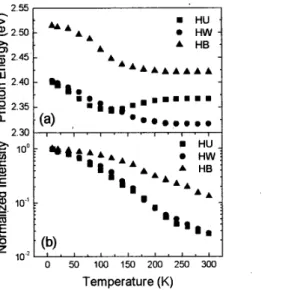
All samples consisted of five QW periods, with 2.5 nm in well width and 7.5 nm in barrier width. Figs. l(a) and (b) show the tempebture-dependent variations of PL spectral peak and normalized integrated PL intensity, respectively, of t h e samples. The three samples are un-doped, well-doped and barrierdoped, denoted with HU, HW, and HB, respectively, with doping concentration of silicon at 5 x 10"
cm".
The nominal indium contents of the three samples are the same at around 20YO.
From part (a), one can see the blue shift of sample HI3 when compared with samples HU and HW. Only sample HU shows a clear S-shape behavior. As shown in Fig. l(b), the radiative efficiency of sample HB is higher than those of the other two samples. Barrierdoped samples always result inhiglier optical qualilji.
2 5 5 1 I
0 50 100 150 200 250 300
Temperature (K)
Fig. 1 (a) Temperature-dependent PL spectral peak positions, and (b) integrated PL intensities of the three samples.
Fig. 2 shows the CL images of the three samples. In samples HU and HW, the sharp sub-micron bright light spots correspond to the indium-rich clusters. The background distributioris of contrast correspond to slowly varying potential fluctuations in the two samples. One can clearly see that slightly more indium-rich clusters but
SigIUficantly stronger potential fluctuation exist in sample HW. This observation
is
consistent with the resultsof
high-resolution TEM images. Compared with samples HU and HW, the CL image of sample HB shows even sharper bright spots and an even stronger potential fluctuation. In particular, more discretelike potential distribution is speculated in sample HB. In other words, distributions of island-like stmctures exist around the QW layers.
Carrier localization and quantum-confined Stark effect (QCSE) are the two major mechanisms for explaining the aforementioned S-shape bellavior. However, it is still unclear which one dominates. With the results above, one can speculate that upon silicon doping in wells or barriers, the QCSE is reduced, due to strain relaxation andor carrier screening, and the S-shape behavior disappears. This argUment actually implies that the usually observed S-shape behavior can be dominated by the QCSE. On the other hand, carrier localization can be the key to the blue shift and
radiative efficiency improvement, particularly in the barrier-doped sample. The similar nano-structures of samples
HU and HW explain well their close PL spectral peak positions, particularly below 150 K, and their close integrated PL intensity curves. The stronger carrier confnement in sample HB does result in higher radiative efficiency. This result may imply that carrier localization is more effective in improving radiative efficiency.
References :
1. Y. C. Cheng, Cheng-Hua Tseng, Chen Hsu, Kung-Jen Ma, Shih-Wei Feng, En-Chiang Lin, C. C. Yang, and Jen-Inn Chyi, “Mechanisms for
2. Y. H. Cho, G. H. Gainer, A. J. Fischer, J. J. Song, S, Keller, U. K. Mishra, and S. P. DenBaars, “S-shaped temperature-dependent emission Photon Emission Enhancement with Silicon Doping in InGaN/GaN Quantum Well Structures,’’ J. Electron. Mater. 32,375-381 (2003). shift and carrier dynamics in InGaN/GaN multiple quantum wells,” Appl. Phys. Lett. 73, 1370-1372 (1998).