0040-6090/02/$ - see front matter䊚 2002 Elsevier Science B.V. All rights reserved. PII: S 0 0 4 0 - 6 0 9 0 Ž 0 2 . 0 0 7 4 3 - 5
Effect of annealing on the structural and optical properties of AgGaS
2thin films prepared by pulsed laser deposition
Hsu-Cheng Hsu, Hsin-hong Chen, Shou-Yi Kuo, Chen-Shiung Chang, Wen-Feng Hsieh*
Institute of Electro-Optical Engineering, National Chiao Tung University, 1001 Tahsueh Road, Hsinchu 30050, Taiwan, ROCReceived 8 August 2002; received in revised form 17 August 2002; accepted 28 August 2002
Abstract
The influence of annealing on the AgGaS films grown by pulsed laser deposition has been investigated. The X-ray diffraction2 results show the AgGaS films were found with preferential orientation2 (1 1 2) normal to the surface and silver droplets were
diminished after the post-annealing. Photoluminescence(PL) measurements reveled the exciton energy is slightly red shifted that
is possibly due to the thermal strain effect. The binding energy of the shallow donors is ;28 meV determined from temperature dependent PL spectra. In addition, the A-exciton and the ByC-exciton could be observed in the transmittance spectra at room
temperature.
䊚 2002 Elsevier Science B.V. All rights reserved.
Keywords: X-ray diffraction; Photoluminescence; Optical properties
1. Introduction
The semiconductor compound AgGaS2 has been extensively studied because of its potential use not only for nonlinear frequency converters but also for photonic devices w1–3x. It has a relatively large nonlinear coef-ficient in wide transparency region from 0.5 to 13 mm and it possesses a wide band gap energy of 2.68 eV at room temperature which is in the blue emission region
w4x. For most applications of photonic device, a suitable
technology for the thin film growth has to be developed. Various methods have been employed for the growth of AgGaS2 films. Pulsed laser deposition (PLD) is a
possible growth technique which has been widely used to fabricate high quality films of multi-element materials such as ferroelectrics and superconductors due to its high-energy flux. Uchiki et al. w5x first reported on the deposition of AgGaS films where a target of consisting2
a stoichiometric mixture of Ag S and Ga S powders2 2 3
has been used. The temperature range was 400–650 8C *Corresponding author. Tel.: q886-3-5712121 ext. 56316; fax: q 886-3-5716631.
E-mail address: wfhsieh@mail.nctu.edu.tw(W.-F. Hsieh).
during the PLD experiment and a XeCl excimer laser was used. However, as shown, the quality of thin film is not good enough to observe exciton emission at low temperature through either photoluminescence (PL) or optical transmittance measurements. Silver particles were always responsible to form precipitates in the film. Recently, a much better film quality was obtained by PLD w6x and multisource evaporation w7x. These films showed exciton features in the PL spectra at low temperature PL and optical reflectance measurements.
As reported in this paper a suitable post-annealing can indeed diminish the silver precipitate formation. Hence, the quality of the PLD-grown AgGaS films can2
be improved. The AgGaS films were grown on quartz2
glass substrates using a KrF excimer laser. Stoichiomet-rically mixed targets of the binary compounds Ag S and2
Ga S have been used. X-ray diffraction2 3 (XRD) results
showed not only the silver XRD peaks have vanished during the annealing process but also the AgGaS2
diffraction width is narrower as previously reported w5– 7x. The observation of A- and ByC-excitons at room
temperature by transmittance measurements also indi-cates an achievement of good film quality.
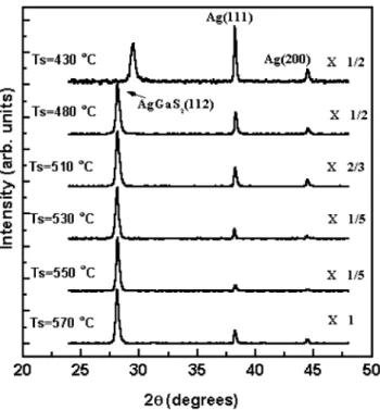
Fig. 1. XRD patterns of the films prepared at different growth temperatures.
Fig. 2. Optical micrographs(1200= magnification) of the film
sur-face of(a) as-grown and (b) annealed films.
2. Experiment
To grow high quality AgGaS films, we used a KrF2
excimer laser(ATLEX-Spi 200) with the wavelength of 248 nm and a pulse duration 4 ns. The laser beam was focused on a target at 458 angle. The pulse energy density of the laser applied was 0.3–0.5 Jycm and the2
pressure in the chamber was kept between 10y5 and 10y6 mbar. The target consists of a stoichiometric mixture of Ag S and Ga S powders which had been2 2 3
pressed into a pellet of 10 mm in diameter. To ensure a good uniformity of the films, the laser beam was scanned over the target and the quartz glass substrate was placed parallel to the target at a distance of 30–40 mm. The substrate temperature varied in the range from 430 to 570 8C.
The surface morphology of the as-grown films was first examined by optical microscopy, and the crystalline quality was evaluated by XRD measurements using Cu Ka (ls1.5406 A, Shimadzu XD-5) radiation. A scan˚ rate of 48ymin in the range from 2us24 to 488 was
applied. The cryogenic PL spectroscopy was carried out using a He–Cd laser operating at 325 nm with the sample being mounted on the cold finger of a low temperature helium cryostat. The PL emission was detected by a monochromator (Jobin Yvon, U-1000)
equipped with a cooled photo-multiplier tube
(Hama-matu R955). The optical transmittance spectra were
measured by means of a HP 8453 spectrometer within the range of 190–1100 nm at room temperature with respect to the bare glass substrate as the reference.
3. Results and discussion
3.1. XRD measurements
Fig. 1 shows the XRD pattern of as-grown films deposited at various substrate temperatures (T ) in thes
range of 2us24–488. All of these films, except for the one grown atT s430 8C, have a main peak at 2u;288.s
They show single-phase of AgGaS with chalcopyrite2
structure and preferred orientation with the(1 1 2) plane
normal to the surface of the glass substrates. From JCPDS (Joint committee on Powder Diffraction
Stan-dards), we found two peaks at approximately 2u;38.3 and 44.58 which are attributed to silver islands that can be observed through an optical microscope as shown in Fig. 2a. We evaluated the film quality via the XRD intensity ratios of AgGaS2 (1 1 2) to Ag (1 1 1). The
effect ofT on the XRD intensity ratios (IAgGaS2yIAg) and
the full widths at the half-maximum (FWHM) of the main peak are listed in Table 1. We found that a good quality of films can be achieved forT ranging betweens
Table 1
The data ofT , Is AgGaS2yI , and the FWHM of the main peakAg
Ts(8C) IAgGaS2yIAg FWHM(8) 510 2.84 0.347 530 5.44 0.318 550 9.14 0.281 560 10.48 0.342 570 4.47 0.343 550 annealed – 0.32
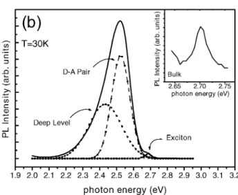
Fig. 4.(a) Temperature-dependence PL spectra of the as-grown film
and(b) PL spectra of the annealed film at 30 K. The inset shows the
PL spectra of the bulk crystal in the exciton region at 30 K.
Fig. 3. XRD for the films as-grown and annealed at 550 8C for 30 min.
550 and 560 8C. We deduced the grain size from XRD according to the Scherrer formula to be 32 nm. Com-paring with the data of pervious work w5–7x, this film seems to have a better quality.
After annealing of the film grown at 550 8C for 30 min, as shown in the optical micrograph of Fig. 2b, the silver droplets seem to disappear apparently. The XRD data also confirmed that the silver diffraction peaks disappeared after thermal annealing as shown in Fig. 3b. In addition, the FWHM of the annealed film (Fig.
3b) is narrower than that of the as-grown one (Fig. 3a).
This indicates the film quality becomes better after heat treatment.
3.2. Photoluminescence measurements
The PL spectra of the as-grown and annealed films grown at T s550 8C are shown in Fig. 4 for thes
measured temperatures ranging from 8.5 to 150 K. We found that the PL spectra of the as-grown films are dominated by a strong green emission below the band gap of the bulk that is centered approximately 506 nm or photon energy of 2.45 eV in Fig. 4a. This peak has been identified as the donor–acceptor pair (DAP)
recombination w8x and was found to disappear above 150 K. Whereas, a weak emission approximately 2.69 eV aside the main peak is observable that can be
attributed to the exciton emission in the annealed sam-ples. All of the temperature dependent PL spectra (not
shown in figure) reveal three main peaks. As shown in Fig. 4b in the PL spectrum measured at 30 K the exciton occurs, a peak caused by DAP, and deep level, respec-tively. The positions of the three peaks are nearly located at the same position independent of the temperature measured. The appearance of exciton emission indicates that the annealed films have better quality than the as-grown ones.
The Arrhenius plots of temperature dependent PL intensities for both as-grown and annealed films are shown in Fig. 5. They can be fitted by the expression:
I(T)sI(0)yw1qa exp(yE yk T)x with I(0), a, and Ea B a
being the fitting parameters and kB the Boltzmann constant. We calculated the activation energies E ofa
Fig. 5. Arrhenius plot of the intensities of the DAP peak at(a)
as-grown film;(b) annealed film.
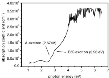
Fig. 6. The transmission spectrum of the annealed AgGaS film meas-2
ured at room temperature.
Fig. 7. The band structure of a typical chalcopyrite semiconductor. thermal decay channels of DAP emissions for the
as-grown and annealed films as 13"3 and 28"2 meV, respectively. They can be attributed to the binding energies of the shallow donor levels below the conduc-tion band. The binding energy of the annealed films is very close to that of AgGaS bulk crystal determined at2
26.8 meV w8x.
In comparison with bulk AgGaS where the exciton2
emission is located approximately 2.70 eV at 30 K, the exciton peak of the annealed film red shifts approxi-mately 12 meV as shown in the inset of Fig. 4b. One may rule out the possibility of quantum size effect that induces blue shift of band edge rather than the observed red shift. Red shift of the exciton emission is consistent with the XRD result that the crystal size evaluated as large as 32 nm. The other reason is presumably the strain effect. The local strain may be induced between the substrate and the grown film during the cooling process due to different thermal expansion coefficients of the materials w9x.
3.3. Optical transmittance
Fig. 6 shows the typical room temperature transmis-sion spectrum of the annealed AgGaS film grown at2 T s560 8C. We used the envelope method w10x tos
estimate the thickness of the film. It was found to be approximately 0.26 mm from the interference feature in the transmission spectrum between 1.25 and 2.5 eV photon energy range. The other two peaks located at 2.67 and 2.96 eV are attributed to the emission of A-and ByC-exciton, respectively. However, we were not
able to resolve the spin–orbit splitting (;8 meV) of
the lower valance bands, i.e. Band C excitons. The band structure of a typical chalcopyrite semiconductor is shown in Fig. 7. The uppermost valence band at the
G point is characterized by the three split bands, G ,7 G6 and G . These splitting is due to the spin–orbit7
interaction (D ) and the non-cubic crystalline fieldso (D ) acting on the threefold degenerate p-like valencecf
band. Under the uniaxial stress quasi-cubic model w1x, the energy of the G valence band relative to the G7 6
valence band,E and E , can be expressed as1 2 1y2 w z 3 2 ŽD qD . y D D
x
so cf so cf|
8 y ~ D qDso cf E s1,2 " . (1) 2 2The three transitions from the valence bands to the
G conduction band are referred as A, Band C transition6
in order of increasing energy. In high-purity semicon-ductors, it is essential to consider the contribution of excitonic absorption from optical absorption spectra. In Fig. 6a, these peaks originate from three allowed direct transitions between the three upper valence bands to the conduction band called A-exciton, B-exciton and
C-exciton peaks. We evaluate the crystal field splitting to be 290 meV, which is very close to the film previously reported w11x and bulk w12,13x results. Since the binding energy of A-exciton is approximately 26 meV w14x, we estimate the band gap of AgGaS is approximately 2.6962
eV at room temperature, which is similar to the finding of other authors w4,5,14,15x. It is indicated that the quantum size effect is not the dominant reason in our experiment.
4. Conclusion
The AgGaS film has been successfully prepared by2
PLD using a KrF excimer laser on quartz glass from a target made of stoichiometric mixture of binary com-pound powders Ag S and Ga S . XRD studies showed2 2 3
that the deposited films were single-phase materials with chalcopyrite structure and preferential texture along
(1 1 2). Moreover, the silver droplets vanished after heat
treatment.
From PL measurement, we found the green emission resulted from the DAP transition. After annealing, the exciton energy is slightly red shifted due to the strain effect. We have determined the shallow donor binding energy in the AgGaS films from the Arrhenius plot of2
temperature dependent PL which is very close to that of bulk crystal. In addition, the A- and ByC-exciton
were estimated at room temperature by analyzing the observed transmittance spectra. It indicates that the post-annealing treatment improves the film quality.
Acknowledgments
This work is partially supported by the National Science Council of the Republic of China under grant No. NSC 90-2112-M-009-050 and 90-E-FA-04 of the Ministry of Education, R.O.C.
References
w1x J.I. Shay, J.H. Wernick, Ternary Chalcopyrite Semiconductors:
Growth, Electronic Properties and Applications, Pergamon Press, New York, 1975.
w2x R.J. Seymour, F. Zernike, Appl. Phys. Lett. 29(1976) 705. w3x D.S. Chemla, P.L. Kasper, D.S. Robertson, R.C. Smith, Opt.
Commun. 3(1971) 29.
w4x L. Artus, Y. Bertrand, J. Phys. C 20(1987) 1365.
w5x H. Uchiki, O. Machida, A. Tanaka, H. Hirasawa, Jpn. J. Appl.
Phys. 32(1993) L764.
w6x H. Uchiki, H. Hirasawa, I. Hasegawa, Jpn. J. Appl. Phys. 33 (1994) L983.
w7x M. Kurasawa, N. Tsuboi, S. Kobayashi, K. Oishi, F. Kaneko,
Jpn. J. Appl. Phys. 38(1999) 1898.
w8x I.H. Choi, P.Y. Yu, J. Phys. Chem. Solids 57(1996) 1695. w9x D.S. Chuu, C.M. Dai, W.F. Hsieh, C.T. Tsai, Appl. Phys. Lett.
69(1991) 8404.
w10x M. Nenkov, T. Pencheva, J. Opt. Soc. Am. A 15(1998) 1852. w11x H.v. Campe, J. Phys. Chem. Solids 44(1986) 1019.
w12x B. Tell, J.L. Shay, H.M. Kasper, Phys. Rev. B 6(1972) 3008. w13x S. Kobayashi, T. Ohno, N. Tsuboi, F. Kaneko, T. Maruyama,
Jpn. J. Appl. Phys. 28(1989) 189.
w14x P.W. Yu, W.J. Anderson, Y.S. Park, Solid State Commun. 13 (1973) 1883.