Effect of Threading Dislocations on Local Contacts in Epitaxial
ZnO Films
C. Y. Lin,a,bW.-R. Liu,a,c,zC. S. Chang,a C.-H. Hsu,a,cW. F. Hsieh,a,d,zand F. S.-S. Chienb,z
a
Department of Photonics and Institute of Electro-Optical Engineering, National Chiao Tung University, Hsinchu 300, Taiwan
b
Department of Physics, Tunghai University, Taichung 407, Taiwan c
National Synchrotron Radiation Research Center, Hsinchu 300, Taiwan d
Institute of Electro-Optical Science and Engineering, National Cheng Kung University, Tainan 700, Taiwan
Local conductance of a ZnO epifilm with a columnar-grain structure was studied by conductive-mode atomic force microscopy. The probe-ZnO junction at the grain boundary with high density edge threading dislocations共TDs兲 behaves as a Schottky contact while the junction at the epitaxial core behaves as an ohmic contact, resulting in the nonuniformity of conductance throughout the film. The calculated Schottky barrier is 0.4⫾ 0.025 eV. The point defects of doubly charged Zn vacancies accumulated at the edge TDs induce local band bending of ZnO, thus contributing to the Schottky nature at the grain boundary.
© 2010 The Electrochemical Society. 关DOI: 10.1149/1.3274825兴 All rights reserved.
Manuscript submitted August 12, 2009; revised manuscript received November 23, 2009. Published January 4, 2010.
ZnO is a promising semiconductor material for various optoelec-tronic applications such as light emitting diodes, transparent con-ducting electrodes, and surface acoustic wave devices1,2due to its large direct bandgap共3.37 eV兲 and exciton binding energy 共60 meV兲 at room temperature. Increasing interest in ZnO was enormously boosted in recent years because of the current advances in the growth techniques, which facilitate the fabrication of high quality ZnO epifilms. Heteroepitaxial ZnO films deposited on lattice-mismatched substrates inevitably contain high density threading dis-locations共TDs兲, which entirely propagate throughout the films. Pre-vious studies indicate that the ZnO epifilms grown on c-plane sapphire feature a columnar-grain microstructure consisting of an epitaxial core共EC兲 encompassed by the small-angle boundary re-gion with high density edge TDs.3TDs can degrade the electric and optical performance of light emitting devices because of the TD-related leakage current.4Moreover, TDs give rise to the defect states in the bandgap, which enhance the deep-level emission共DLE兲 in the photoluminescence 共PL兲 spectra.5 These defect states can be par-tially occupied by negative charges until their energy共Edis兲 reaches the Fermi energy of ZnO.6The negatively charged TDs in semicon-ductors have been verified by transmission electron microscopy 共TEM兲 7
and scanning capacitance microscopy.3,8 Negatively charged TDs can also result in some unusual effects at the metal– ZnO contacts. A reliable and low resistance ohmic-contact metalli-zation is highly expected for device applications.9Although several efforts have been devoted to investigate the properties of common metal–ZnO contacts subjected to thermal,10 plasma,11 and UV 12 treatments, few studies were focused on the local properties of metal–ZnO contacts. Therefore, it is crucial to study how TDs lo-cally influence the band structure and conductance at the contacts.
In this study, we applied conducting atomic force microscopy 共CAFM兲 to analyze the local contact to the epitaxial ZnO films. The CAFM measurements have been described elsewhere.13,14Briefly, a conducting tip scans at a constant contact force over the surface and acts as an electrode to collect the local current through the probe-ZnO junction. The local current–voltage共I-V兲 characteristics reveal that the contact in the EC region behaves as an ohmic contact but that in the boundary region shows a Schottky one. The filling of the dislocation states by negative charges leads to the bending of the conduction band共CB兲 in the vicinity of the TD lines, thus forming a Schottky barrier. Considering the position of Edis, 0.4⫾ 0.025 eV
below the ZnO conduction band minimum共CBM兲, we attribute Edis to the negatively charged Zn vacancies共VZn2−兲.
Experimental
The ZnO epifilms with a thickness of approximately 1.2 m were grown on 共0001兲 sapphires by pulsed laser deposition 共PLD兲. The details of the growth conditions and the structure of ZnO epifilms were reported elsewhere.3,8 The carrier density ne, mobility, and resistivity are 3.3⫻ 1017 cm−3, 12 cm2 V−1 s−1, and 1.6 ⍀ cm, respectively, as obtained by Hall measurement. The X-ray diffraction共XRD兲 measurements were performed with a four-circle diffractometer at the wiggler beamline BL13A of the National Synchrotron Radiation Research Center, Taiwan, with an incident wavelength of 1.02735 Å. The topographic and current mappings as well as the local I-V characteristics were measured by a scanning probe system共Agilent 5500 AFM兲 with Cr–Pt coated cantilevers. The PL measurements were carried out with a 325 nm He–Cd laser. The light emission spectrum was measured by a Triax-320 spec-trometer equipped with a UV-sensitive photomultiplier tube.
Results and Discussion
Structural analysis of XRD and PL.— The -rocking curve of
the ZnO共0006兲 reflection was measured, as shown in Fig.1a. The obtained mosaic spread of the ZnO film is 0.0564°, which strongly supports the good crystalline quality of the ZnO epilayers. The lattice parameters of the ZnO layer are a = 3.244 Å and c = 5.221 Å, which were determined by fitting the positions of sev-eral Bragg reflections. Compared to the bulk values of a ZnO wafer,
a = 3.249 Å and c = 5.206 Å, the ZnO epitaxial films experience a
tensile strain共⬃0.28%兲 along the normal to the surface and a com-pressive strain共⬃0.15%兲 along the lateral direction. The tilting and twisting angles as well as the coherence lengths along the normal to the surface and lateral direction are 0.052 and 0.19° and 519 and 90 nm, respectively, extracted from the analysis of the Williamson–Hall plot.3The TD densities of the edge and screw types calculated from the XRD data are 5.5⫻ 109and 7⫻ 107 cm−2, respectively, which
implies that the edge type is dominant in the film. The PL spectrum at room temperature, as shown in Fig.1b, exhibits a very weak DLE and a narrow near-band edge共NBE兲 emission at 3.305 eV with a full width at half-maximum共fwhm兲 of ⬃80 meV, which is dominated by the free exciton emission. The narrow NBE emission and low DLE are a signature of good optical performance. Therefore, both the XRD and PL results corroborate the high quality of ZnO films.
Common metal–ZnO contact by Pt electrodes.— The I-V
char-acteristic of a common Pt–ZnO contact indicates an ohmic contact, as shown in Fig.2a. The top Pt electrode was deposited by sputter-ing. The band diagram of Pt and ZnO共Fig.2b兲 shows a significant gap between the Fermi energy of Pt共EF兲 and the CBM of ZnO, z
E-mail: [email protected]; [email protected]; [email protected]
Journal of The Electrochemical Society, 157共3兲 H268-H271 共2010兲
0013-4651/2010/157共3兲/H268/4/$28.00 © The Electrochemical Society H268
) unless CC License in place (see abstract).
ecsdl.org/site/terms_use
address. Redistribution subject to ECS terms of use (see
140.113.38.11
suggesting the Schottky nature of the contact. However, several ex-amples of metal–ZnO ohmic contacts, such as Au on commercial undoped ZnO substrates11 and Ti or Ni on PLD-grown ZnO epifilms,15 have been reported. The degradation of rectification of the metal–ZnO contacts is attributed to the absorption of OH−ions on the ZnO surface. It results in the downward band bending of ZnO, producing a conductive accumulation layer at the surface. Therefore, the conducting property of ZnO films can be treated as a bilayer system, i.e., the surface layer and the bulk.16 The carrier density in the surface layer 共nse兲 could be as high as 5.3
⫻ 1020 cm−3and that in the bulk共n
be兲 is 2.5 ⫻ 1016 cm−3.12The
width of the depletion layer is several nanometers only for the high carrier density of the surface layer, as shown in Fig.2c. Therefore, tunneling becomes the dominant mechanism of carrier transport, leading to the ohmic behavior of the metal–ZnO contacts.
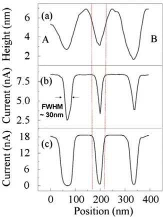
Local metal–ZnO contacts by metal-coated probes.— Figure 3a is the topographic image of the ZnO surface taken by atomic force microscopy共AFM兲. Figure 3b and c is current mappings under a forward bias of 0.5 V and a reverse bias of⫺1.5 V, respectively. The conductance of the film is nonuniform, and there is a strong corre-lation between the topographic and current images, i.e., the locations of current dips coincide with the grain boundaries under both the forward and reverse biases. Figure4shows the cross-sectional pro-files along the line共A to B兲 marked in Fig.3. Although the dips of the current coincide with that of topography, the width of current dips noticeably differs from that of topographic dips. The fwhm of current dips is⬃30 nm. The mean intergrain spacing is about 120 nm, obtained from the Fourier transformation of Fig. 3a, as the lateral coherence length derived from XRD is about 90 nm. The
difference between these two lengths yields the 30 nm fwhm of the boundary region. Therefore, it can be concluded that the current dip is due to the edge TDs in the grain boundaries.
The local I-V curves taken by a CAFM probe on the EC and grain boundary are shown in Fig.5. An ohmic contact is observed in the EC region, consistent with the result of the common Pt–ZnO contact. However, the contact at the boundary exhibits a Schottky nature. We fitted the I-V curve using the typical expression of ther-mionic emission17,18
I = AAⴱT2 exp
冉
−qBkT
冊
冋
exp冉
qVkT
冊
− 1册
关1兴where A denotes the area of the contact, Aⴱis the effective Richard-son constant 共⬃32 A cm−2 K−2 and mⴱ⬃ 0.27m
0兲, B is the
Schottky barrier height, k is the Boltzmann constant, T is the abso-lute temperature共300 K兲, and is the ideality factor. We obtained B= 0.4⫾ 0.025 eV and is ⬃5, assuming that the contact area
is ⬃1000 nm2. The high value elucidates that the transport
mechanism is not only thermionic emission but also tunneling. The Schottky behavior is attributed to the TD-related band bending and B=⌬Edis 共⌬Edis= Edis− ECBM is the depth of the dislocation
states兲. It implies that the depth of the dislocation states is 0.3–0.4 eV below ECBMof ZnO. Consequently, the CB potential barrier is
several tenths of an eV, and the acceptor-like states associated with edge TDs locate near the CBM.
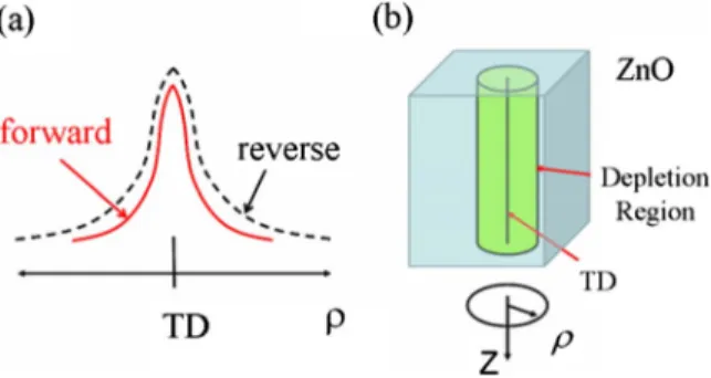
The edge TDs of n-type ZnO were investigated by phase recon-struction of electron waves in TEM.7A distinct phase shift of the transmitted electron wave induced by the local potential, generated by the charged dislocation line and associated screening of charges, was recognized; but no phase shift was observed in pure screw TDs. The edge TDs behave as acceptor-like trap states with negative charges in the cylinders of radius d with its axis along the disloca-tion lines, where d is of several angstroms. Tivarus et al. calculated the local CB bending at the edge TDs line close to a metal– semiconductor interface, as shown in Fig. 6a.19The existence of negatively charged edge TDs leads to the carrier depletion in the space charge cylinders around the vicinity of the TD line共shown in Fig.6b兲, which accounts for the Schottky nature at the boundary and
Figure 2.共Color online兲 共a兲 I-V curve of the normal contact between the Pt
electrode and the ZnO epifilm and关共b兲 and 共c兲兴 band diagrams of Pt and ZnO films with the absorption of OH ions at the surface before and after contact, respectively.
Figure 1. 共Color online兲 共a兲 -rocking curve of the ZnO共0006兲 reflection
and共b兲 PL spectrum measured at room temperature.
H269
Journal of The Electrochemical Society, 157共3兲 H268-H271 共2010兲 H269
) unless CC License in place (see abstract).
ecsdl.org/site/terms_use
address. Redistribution subject to ECS terms of use (see
140.113.38.11
the conductance mismatch between the EC and boundary region. The radius of the space charge cylinder R can be obtained from the expression7
R = d
冑
ndisnbe 关2兴
Given that nbe, the density of trapped charges 共ndis兲,7 and d are
2.5⫻ 1016 cm⫺3, 5⫻ 1019 cm⫺3, and 0.5 nm, respectively. The
calculated diameter共R兲 of the cylinder is ⬃22 nm. R is close to the width of the grain boundary obtained from the cross-section profile
Figure 3.共Color online兲 共a兲 AFM topographic image of the ZnO film and the
corresponding current mapping images taken under共b兲 a forward bias of 0.5 V and共c兲 a reverse bias of ⫺1.5 V.
Figure 4. 共Color online兲 共a兲 Cross-sectional profiles AFM topography and
CAFM current under共b兲 forward bias and 共c兲 reverse bias along the line indicated from A to B in Fig.3. The dashed lines show the region of the grain boundary.
Figure 5. 共Color online兲 Local I-V characteristics taken by CAFM on the
grain boundary. The current amplifier is saturated beyond⫾28 nA. H270 Journal of The Electrochemical Society, 157共3兲 H268-H271 共2010兲
H270
) unless CC License in place (see abstract).
ecsdl.org/site/terms_use
address. Redistribution subject to ECS terms of use (see
140.113.38.11
of CAFM. This strongly supports that the dips in current mapping are due to the existence of edge TDs.
From both the CAFM images and current profiles, we observed that the width of the current dips becomes wider when a reverse bias is applied. The reverse bias builds an electric field at the Pt–ZnO interface and causes the decrease in nbe. According to Eq. 2, R
increases as nbe decreases, assuming that ndis is fixed. Effectively, the width of the potential barrier extends with the reverse bias, as illustrated in Fig.4a.
Assuming that the TDs are electrically inactive and the point defects are accumulated around the dislocation lines caused by the strain field,20we suggest that the trapped charges are associated with the point defects. The most abundant native defects in ZnO are the acceptor-like Zn vacancies 共VZn兲 and the donorlike O vacancies
共VO兲, according to the calculation using the first-principles
pseudo-potential method.21 Here we propose that the defects are doubly charged Zn vacancies共VZn2−兲 based on the following facts. First, O vacancies tend to be neutral or positively charged, so VO is
ex-cluded. Second, the Fermi level of the native n-type ZnO is very close to the CBM so that VZn2−has the lowest formation energy and the estimated energy level of VZn2−is about 0.4–0.5 eV below ECBM,22 which agrees with our prediction from the I-V characteristics. As the density of VZn2−is sufficiently high, the Fermi level of ZnO is pinned to the defect level of VZn2−, resulting in the Schottky contact.
ZnO has the same crystal structure as GaN, both belonging to the space group P63mc. The main defect structures of epitaxial ZnO and
GaN films on sapphire substrates are edge TDs. The dislocations are negatively charged in both films.7,23However, the electronic behav-ior of TDs in these films is different. Unlike the Schottky barrier formed at the edge TDs in ZnO films, there is no evidence to show that the edge TDs in GaN significantly affect the current conduction as studied by the probe techniques.14,23The charged edge TDs in GaN films should also induce a potential barrier as the theoretical prediction and the analysis of phase reconstruction. The CAFM mapping of GaN may be insensitive to the small variation in poten-tial due to the charged TDs, whereas the probe GaN is a Schottky contact and the defect states are shallow. In contrast to the ohmic Pt–ZnO contact observed in the grain center, one can distinguish the Schottky contact at the edge TD regions from the ohmic back-ground. However, the screw TDs also behave differently in ZnO and GaN films. The screw TDs in GaN introduce leakage paths for the
current measured by CAFM, but we did not observe any leakage or other trace of the minor screw TDs in the ZnO film. Further study is therefore necessary to understand the origin of the difference.
Conclusion
The influence of the edge TDs on the electrical properties of the ZnO epifilm grown by PLD on 共0001兲 sapphire was studied by CAFM. The strong correlation between the spatial distribution of TDs and current dip indicates that the edge TDs are negatively charged. The increase in the conduction band in the vicinity of the TDs leads to the Schottky behavior of the Pt–ZnO contact. The bending of the conduction band is caused by the point defects of VZn2− accumulated along the TD lines, and the defect level of VZn2− is 0.4⫾ 0.025 eV below the conduction band maximum.
Acknowledgments
The authors gratefully acknowledge the support of the National Science Council of Taiwan by NSC contracts 96-2112-M-029-005-MY3 and 97-2112-M-009-013.
Tunghai University assisted in meeting the publication costs of this ar-ticle.
References
1. A. Tsukazaki, A. Ohtomo, T. Onuma, M. Ohtani, T. Makino, M. Sumiya, K. Ohtani, S. F. Chichibu, S. Fuke, Y. Segawa, et al., Nature Mater., 4, 42共2004兲. 2. X. Y. Du, Y. Q. Fu, S. C. Tan, J. K. Luo, A. J. Flewitt, W. I. Milne, D. S. Lee, N.
M. Park, J. Park, Y. J. Choi, et al., Appl. Phys. Lett., 93, 094105共2008兲. 3. W.-R. Liu, W. F. Hsieh, C.-H. Hsu, K. S. Liang, and F. S.-S. Chien, J. Appl.
Crystallogr., 40, 924共2007兲.
4. X. A. Cao, J. M. Teetsov, M. P. D. Evelyn, D. W. Merfeld, and C. H. Yan, Appl. Phys. Lett., 85, 7共2004兲.
5. W.-R. Liu, Y.-H. Li, W. F. Hsieh, C.-H. Hsu, W. C. Lee, M. Hong, and J. Kwo, J. Phys. D: Appl. Phys., 41, 065105共2008兲; J. H. You and H. T. Johnson, J. Appl. Phys., 101, 023516共2007兲.
6. H. Alexander and H. Teichler, Materials Science and Technology, Vol. 4, Chap. 6, p. 249, North-Holland, Amsterdam共1991兲.
7. E. Müller, D. Gerthsen, P. Brückner, F. Scholz, Th. Gruber, and A. Waag, Phys. Rev. B, 73, 245316共2006兲.
8. W.-R. Liu, W. F. Hsieh, C.-H. Hsu, K. S. Liang, and F. S.-S. Chien, J. Cryst. Growth, 297, 294共2006兲.
9. A. A. Iliadis, R. D. Vispute, T. Venkatesan, and K. A. Jones, Thin Solid Films, 420–421, 478共2002兲.
10. H. S. Yang, D. P. Norton, S. J. Pearton, and F. Ren, Appl. Phys. Lett., 87, 212106 共2005兲.
11. H. L. Mosbacker, Y. M. Strzhemechny, B. D. White, P. E. Smith, D. C. Look, D. C. Reynolds, C. W. Litton, and L. J. Brillson, Appl. Phys. Lett., 87, 012102共2005兲. 12. Y.-J. Lin, C.-L. Tsai, W.-R. Liu, W. F. Hsieh, C.-H. Hsu, H.-Y. Tsao, J.-A. Chu, and
H. C. Chang, J. Appl. Phys., 106, 013701共2009兲.
13. P.-J. Gallo, A. J. Kulik, N. A. Burnham, F. Oulevey, and G. Gremaud, Nanotech-nology, 8, 10共1997兲.
14. J. W. P. Hsu, M. J. Manfra, R. J. Molnar, B. Heying, and J. S. Speck, Appl. Phys. Lett., 81, 79共2002兲.
15. C.-L. Tsai, Y.-J. Lin, Y.-M. Chin, W.-R. Liu, W. F. Hsieh, C.-H. Hsu, and J.-A. Chu, J. Phys. D: Appl. Phys., 42, 095108共2009兲.
16. D. C. Look, H. L. Mosbacker, Y. M. Strzhemechny, and L. J. Brillson, Superlat-tices Microstruct., 38, 406共2005兲.
17. S. M. Sze, Physics of Semiconductor Devices, 2nd ed., Chap. 5, John Wiley & Sons, Englewood Cliffs, NJ共1981兲.
18. S. H. Kim, H. K. Kim, and T. Y. Seong, Appl. Phys. Lett., 86, 112101共2005兲. 19. C. Tivarus, Y. Ding, and J. P. Pelz, J. Appl. Phys., 92, 6010共2002兲.
20. J. Elsner, R. Jones, P. K. Sitch, V. D. Porezag, M. Elstner, T. Frauenheim, M. I. Heggie, S. Öberg, and P. R. Briddon, Phys. Rev. Lett., 79, 3672共1997兲. 21. A. F. Kohan, G. Ceder, D. Morgan, and C. G. Van de Walle, Phys. Rev. B, 61,
15019共2000兲.
22. F. A. Kröger, The Chemistry of Imperfect Crystals, 2nd ed., Vol. 2, North-Holland, New York共1984兲.
23. B. S. Simpkins, E. T. Yu, P. Waltereit, and J. S. Speck, J. Appl. Phys., 94, 1448 共2003兲.
Figure 6.共Color online兲 共a兲 Potential diagram of the local conduction band
bending near a negatively charged TD line as a function of the distance from the dislocation line under forward and reverse biases and共b兲 schematic of a charged TD line and the depletion region.
H271
Journal of The Electrochemical Society, 157共3兲 H268-H271 共2010兲 H271
) unless CC License in place (see abstract).
ecsdl.org/site/terms_use
address. Redistribution subject to ECS terms of use (see
140.113.38.11